Designing of spin filter devices based on zigzag zinc oxide nanoribbon modified by edge defect∗
2019-11-06BaoRuiHuang黄保瑞FuChunZhang张富春YanNingYang杨延宁ZhiYongZhang张志勇andWeiGuoWang王卫国
Bao-Rui Huang(黄保瑞),Fu-Chun Zhang(张富春),Yan-Ning Yang(杨延宁),Zhi-Yong Zhang(张志勇),and Wei-Guo Wang(王卫国)
1School of Information Science Technology,Northwest University,Xi’an 710127,China
2School of Physics and Electronic Information,Yan’an University,Yan’an 716000,China
Keywords:ZnO nanoribbon,spin-dependent transport,nonequilibrium Green’s functions,transmission eigenchannels,spin filtering efficiency
1.Introduction
Spintronics is a promising field for the next-generation electronic devices,which have lower energy consumption and faster electronic systems due to the use of electron intrinsic spin states to carry information.[1–3]Although spinbased electronic devices are currently used in commercial magnetic-field sensors and nonvolatile memory devices,[4]the spin states in the transport process are a major challenge in the field of spintronics because spin–orbital coupling and scattering can change their intrinsic spin state.[5]A spin filter is an important device for processing spin states. Currently,spin filters are based on carbon atomic chains,[6]Josephson junctions,[7]ferromagnetic quantum barriers,[8,9]molecular devices,[10]graphene nanoribbons,[11–14]and graphite-like nanoribbons.[15,16]
ZnO,a group II–VI compound semiconductor,has unique properties and novel applications in photocatalysis, spintronics,and photovoltaics.[17]Bulk ZnO has a direct wide band gap(3.37 eV),large exciton binding energy(60 meV),high optical gain(320 cm−1), strong luminescence, high electron mobility,superior piezoelectric properties,and high transparency.[18–20]In addition,various ZnO structural forms have been synthesized such as nanosheets,[21]nanotubes,[22]nanowires,[23]nanorods,[24]and nanoribbons.[25]A nanoribbon is a one-dimensional nanostructure with its thickness much smaller than its width.The ZnO nanoribbon(ZnONR)can be obtained by cutting the graphite-like ZnO nanosheets.On the basis of the shapes of the edges,ZnONRs are divided into armchair and zigzag ZnONRs, both of which have stable structures.[26,27]Recently,nanoribbons have attracted considerable attention because graphene nanoribbons exhibit perfect spin-filtering properties,and some graphenelike nanoribbons(e.g.,silicon nanoribbons[28]and boron nitride nanoribbons[29])also possess filtering properties. The ZnO nanoribbon has a graphene-like structure,and its electronic structure and magnetic properties depend on its orientation.The armchair ZnONR is a nonmagnetic semiconductor with a band gap that changes with its width,while the zigzag ZnONR is a ferromagnetic metal.[30]Because magnetism is essential for the spin-dependent transport,ZnONR is expected to exhibit an interesting spin-dependent transport.The electronic transport of ZnONR has been reported by Sarkar et al.,[31]and Zhang et al.[32]determined that the zigzag ZnONR with edges passivated by zinc atoms maintains an absolute spin filter effect in a larger bias range.In addition,there are no reports on spin-dependent ZnONR transport,and none of the effects of defects,doping,edge states,and external electromagnetic field is clear.Therefore,it is strongly motivated to exploring their transport phenomena and mechanisms.
In this work,we focus on the spin-dependent electronic transport of zigzag ZnONR.It is determined that the zigzag ZnONR exhibits a complete spin-polarized transport,and a NDR behavior can be observed for the spin-down current.A further analysis indicates that the spin-up transmission is mainly determined by the Zn 4s at the edge of the ZnONR.Moreover,ZnONR modified by the Zn-edge defect demonstrates a perfect spin-filtering effect,which has a considerable application potential.We believe that our results are quite useful for developing a spin filter based on ZnONR.
2.Computational methods
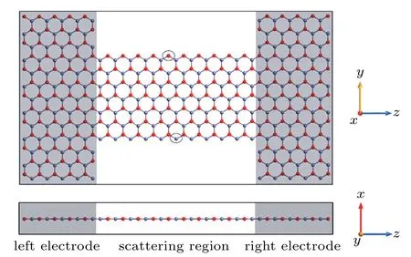
The model of a two-probe device is constructed by cutting a ZnO monolayer with zigzag edges as illustrated in Fig.1.The width of ZnONR is defined by the number of parallel zigzag Zn–O chains,and n-ZnONR denotes a zigzag ZnONR with n Zn–O chains. To investigate the electronic structure and transport properties,the device is divided into three regions:left electrode,right electrode,and central scattering region.In our calculations,the geometry of the ZnO monolayer is carried out by using the plane-wave pseudopotential total energy calculation method based on density function theory(DFT)as implemented in the Cambridge sequential total energy package(CASTEP).The exchange–correlation potential is treated by the generalized gradient approximation(GGA)with Perdew and Wang 91(PW91)parameterization scheme.The interaction between nuclei and electrons is approximated with Vanderbilt ultrasoft pseudopotential.The plane-wave basis set has cutoff energy of 480 eV,and the Brillouin zone integration is approximated by using a 6×6×1 Monkhorst–Pack k-point mesh. The convergence tolerance is set to be 1×10⁻⁵eV/atom and the vacuum layer is set to 15 ˚A to avoid the interaction between adjacent layers.

Fig.1.Schematic illustration of device model:the gray region denotes the left and right electrodes,and the transport direction is in z direction. Periodic boundary conditions are applied along x and y directions,and 15-˚A vacuum spacing is in x direction to avoid the interaction between adjacent layers.Gray circles indicate sites of the edge defects.Red and gray spheres represent oxygen and zinc atoms,respectively.
The spin-dependent transport properties are performed by the QuantumWise Atomistix Toolkit(ATK)package. This package combines DFT with non-equilibrium Green’s function(NEGF)to simulate spin-polarized quantum transport in the non-equilibrium case.The exchange–correlation potential is described by Perdew–Burke–Ernzerhof(PBE)parametrization of GGA.The basis set of the linear combination of atomic orbital uses double zeta polarization for all atoms,and the iteration control parameter uses mesh cutoff energy of 150 Ry with a tolerance of 1×10⁻⁵.The two-dimensional(2D)fast Fourier transform(FFT2D)is applied to the investigation of periodic boundary conditions. The Monkhorst–Pack k-point grid of 1×1×100 is employed in the transport calculation.The k-point sampling of 1,1,and 100 is used in the x,y,and z directions,respectively,where z refers to the direction of charge transport.Spin-dependent transmission values through the nanoribbon at the given energy and the spin electron transmission coefficient under external bias Vbare obtained from the following equation[33,34]

where the spin index σ indicates spin-up or spin-down;ΓL/ΓRis the conductor’s coupling function to the left/right electrodes,E is the electronic energy,and Gr/Gais the retarded/advanced Green’s function of the scattering region.The spin-dependent current of device is calculated from the Landauer–Büttiker formula[35,36]

where e is the electron charge,h is the Planck’s constant,and fL/R(E,Vb)is the Fermi–Dirac distribution function of left/right electrode.The difference in chemical potential between the left electrode and the right electrode isµL−µR=eVb.When the Fermi level is set to be zero,the bias voltage window corresponds to the range[−Vb/2,+Vb/2].
3.Results and discussion
First,we take 7-ZnONR for example to investigate the spin-dependent electronic transport properties.The two-probe device based on pristine 7-ZnONR is constructed as illustrated in Fig.1,and named M1. For M1,the corresponding spindependent transmission spectra T(E,Vb)at zero bias voltage are plotted in Fig.2(a). It is clearly observed that the spindown and spin-up transmission spectrums do not coincide with each other.The transmission is spin-polarized,which results in the dangling bonds of atoms at the edge of ZnONR.At−0.26 V and −0.28 V,there are minimum spin-up and maximum spin-down transmission spectrums,respectively.Near the Fermi level,there are wide spin-up and spin-down transmission platforms,and the spin-up transmission coefficient is lower than the spin-down coefficient.This indicates that both spin transmission channels are open at the Fermi level. To elucidate the mechanism of transmission channels,we investigate the spin-polarized band structure,projected density of states(PDOS),and Bloch states of ZnONR as shown in Fig.3.By comparing the spin-up band with spin-down band,we observe the splitting of these bands around the Fermi level as illustrated in Fig.3(a),which is marked as I,II,and III.It is observed that only one band crosses the Fermi level in the spin-up case,and three bands cross the Fermi level in the spindown case.According to PDOS in Fig.3(b),the 2p state of O atom and the 4s state of Zn atom are asymmetric in spin-up and spin-down cases.Thus,spin splits in the Fermi level originate from O 2p and Zn 4s.The calculated results are in agreement with those previously published results.[37]For each spin,the distributions of Bloch states are in accordance with those of the eigenchannels.We calculate the Bloch states of the three bands,and the results are plotted in Fig.3(c).It is determined that all Bloch states are distributed at the edge of ZnONR.Notably,regardless of the spin-up or spin-down,the Bloch states of the band marked as I are located in the Zn-edge.The Bloch state bands,marked as II and III are located at the O-edge in the spin-down case,and there are no Bloch states in the spinup case.According to the above-mentioned analysis,the spin transport channel is provided by O 2p and Zn 4s at the edge of ZnONR.

Fig.2.Spin-dependent transmission spectra T(E)at zero bias voltage for(a)M1,(b)M2,and(c)M3,respectively.Zero of energy is set to be at Fermi level.

Fig.3.(a)Spin-polarized band structure of 7-ZnONR;(b)spin-polarized PDOS of 7-ZnONR,Fermi level is set to be at zero;(c)Spin-polarized Bloch states of energy bands I,II,III,respectively,with isovalue being 0.2.
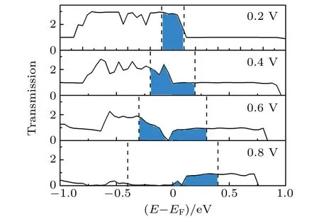
To investigate the transport properties of 7-ZnONR under applied bias,the spin-dependent current–voltage(I–V)curve of M1is shown in Fig.4(a).At the bias from 0 V to 1.0 V,we clearly observe that the current is spin-polarized.For the spin-up case,the current increases slowly with bias voltage increasing.When the electron is of spin-down,the spin-down current is proportional to the bias voltage in a range from 0 to 0.2 V,but then oscillates slightly in a range from 0.2 V to 0.6 V.The spin-down current peak value is 23.2µA at 0.58 V.With the bias further increasing,the spin-down current decreases rapidly to 8.7µA at 0.84 V.It is clearly seen that the NDR has a peak-to-valley ratio of 2.7.Moreover,to obtain a clear picture about the mechanism of the NDR effect,the transport spectra for the spin-down electrons at 0.2,0.4,0.6,and 0.8 V are displayed in Fig.5.According to Eq.(2),the T(E,Vb)in the bias voltage window determines the current,and the integrated area in the window is displayed as a shaded area.At a bias voltage of 0.2 V,there is a high transmission plateau in the bias window.As the bias voltage increases,the transmission spectrum is suppressed.Then,although the amplitude of the transmission spectrum lowers,the bias window increases.There is almost no change in the integrated area,thus redsulting in a current plateau in a bias range of 0.2 V–0.6 V.When the bias reaches 0.8 V,the transmission spectra are severely suppressed. The increase in the bias window range cannot compensate for the decrease in the integral area caused by the decrease in the transmission coefficient,which leads the strong NDR to occur.

Fig.4.Plots of spin-up and spin-down currents versus voltage at zero bias voltage for(a)M1,(b)M2,and(c)M3,respectively.

Fig.5.Variations of spin-down transmission coefficient with E of M1 at 0.2,0.4,0.6,and 0.8 eV,respectively,with blue shade between dashed lines being integral area of spin-down current.Zero of energy is set to be at Fermi level.
It is known that for M1,the edge states are essential for the electronic spin transport.If the edge Bloch states are destroyed,the spin-filtering effect may occur.In fact,the edge defect of the nanoribbon is an effective approach to destroying the edge Bloch states.To explore the spin filter based on ZnONR,we construct the two-probe devices based on ZnONR with edge defects.In Fig.1,the gray circles indicate the sites of the edge defects.The devices with the O-edge and Zn-edge defects are denoted as M2and M3,respectively.When the O or Zn atom is removed,the geometries are optimized again to obtain the relaxed structures.For the O-edge defect case,the transmission spectrum is illustrated in Fig.2(b).By comparing the transmission of M1in Fig.2(a),we find that the spinup transmission coefficient remains approximately unchanged near the Fermi level,whereas the spin-down transmission coefficient decreases from 3 to 1.The difference in transmission coefficient between spin-up and spin-down cases is reduced,and the corresponding I–V curves are similar to each other as illustrated in Fig.4(b). For the Zn-edge defect case,the transmission spectrum is illustrated in Fig.2(c).Comparing with Fig.2(a),the transmission coefficient exhibits a decreasing behavior near the Fermi level.The spin-up transmission coefficient decreases from 1 to 0,and the spin-down transmission coefficient decreases from 3 to 2.Meanwhile,the spindown current is clearly larger than the spin-up current in the bias voltage region as shown in Fig.4(c).Therefore,the M3system acts as a perfect spin filter.The polarization characteristics of spintronic device can be quantitatively described by the spin-filtering efficiency(SFE).The SFE at non-zero bias is calculated by the spin-dependent current as follows:

The SEF at zero bias is calculated by the spin-dependent transmission coefficient at zero bias below.

The calculated SFEs for the three systems are shown in Fig.6.It is clear that the SFEs of M1,M2,and M3at zero voltage are 57%,11%,and 100%,respectively.For M1,the SFE decreases continuously with bias increasing.For M2,the SFE is less than 10%in the whole bias range.However,M3has a high SFE in the entire bias range,reaching approximately 100%at[0 V,0.3 V],which indicates that M3is an ideal spin-filtering device.

Fig.6.Plots of SFE versus bias voltage for M1,M2,and M3.
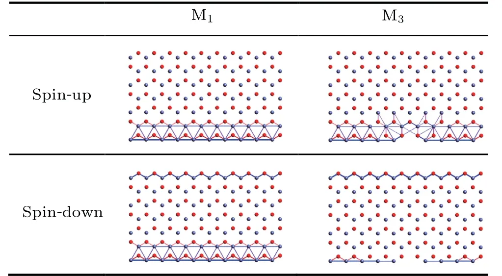
To investigate the effect of the defects on the transport properties of ZnONR,figure 7 shows the electron transport pathways for the spin-up and spin-down states of M1and M3under zero bias.The transport pathways can analyze the contribution of local bonds to the transmission coefficient.[38]As illustrated in Fig.7,the direction of the transport pathways is indicated by colored arrows(e.g.,blue and purple arrows point to the right,and red arrows point to the left).The size of the arrows indicates the magnitude of the transport pathways.There are two types of transmission channels:one is a chemical bond between zinc and oxygen,and the other is a hopping channel between the same atoms.This phenomenon also occurs in the devices that are based on MoS2.[39]Figure 7 indicates that the transmission occurs mainly through the edges of ZnONR and reaches the other electrode.This observation is consistent with the result of the Bloch state analysis in Fig.3.For M1,the spin-up electrons are transferred through the Zn atoms located at the Zn edge.Concurrently,some of the electrons are reflected to the left electrode by the Zn–O bond. When the Zn-edge defects are generated,the spin-up electron transport channels are destroyed,and the spin-up electrons are strongly scattered near the defects. Therefore,the spin-up current is severely suppressed. However,for the spin-down electrons,there are two spin-down transport channels,which are located at the zinc and oxygen edges. The Zn-edge transport channel is aligned with the spin-up transport channel,and the Oedge transport channel is composed of Zn–O bonds.When the Zn-edge defects are generated,the spin-down transport channel of the zinc edge completely disappears.Accordingly,the spin-down transport channel remains constant at the edge of oxygen. Therefore,in M3,the spin-up transport channel is severely damaged or suppressed,and the spin-down transport channel is preserved.

Fig.7.Transport pathways for spin-up and spin-down states of M1 and M3 under zero bias.
4.Conclusions
In this work,by using first principle based on DFT combined with NEGF,we studied the electronic structure of intrinsic ZnONR.By analyzing the band structure,split-state density,and Bloch states,we reveal that the energy bands of ZnONR exhibit spin splitting near the Fermi level.The spindown current has a significant NDR effect. In addition,the Bloch state of the energy band of the spin splitting is distributed at the edge of ZnONR.By using the edge defect modulation,we constructed M2and M3devices.The SFE of M3demonstrates that it has a perfect spin-filtering effect.The M3device,which possesses a simple structure without stacked layers and external magnetic-field regulation,can be used to fabricate a spin filter.
猜你喜欢
杂志排行
Chinese Physics B的其它文章
- Compact finite difference schemes for the backward fractional Feynman–Kac equation with fractional substantial derivative*
- Exact solutions of a(2+1)-dimensional extended shallow water wave equation∗
- Lump-type solutions of a generalized Kadomtsev–Petviashvili equation in(3+1)-dimensions∗
- Time evolution of angular momentum coherent state derived by virtue of entangled state representation and a new binomial theorem∗
- Boundary states for entanglement robustness under dephasing and bit flip channels*
- Manipulating transition of a two-component Bose–Einstein condensate with a weak δ-shaped laser∗
