A review of current research on spin currents and spin–orbit torques∗
2019-11-06XiaoYuFeng冯晓玉QiHanZhang张琪涵HanWenZhang张瀚文YiZhang张祎RuiZhong钟瑞BoWenLu卢博文JiangWeiCao曹江伟andXiaoLongFan范小龙
Xiao-Yu Feng(冯晓玉),Qi-Han Zhang(张琪涵),Han-Wen Zhang(张瀚文),Yi Zhang(张祎),Rui Zhong(钟瑞),Bo-Wen Lu(卢博文),Jiang-Wei Cao(曹江伟),and Xiao-Long Fan(范小龙)
The Key Laboratory for Magnetism and Magnetic Materials of Ministry of Education,Lanzhou University,Lanzhou 730000,China
Keywords:spin–orbit coupling,pure spin current,spin–orbit torques,physical effects associated with spin current
1.Introduction
Spintronics is an emerging discipline of research involving the application of electronic spin properties.[1]Spin is a relativistic effect,which was first considered when Dirac wrote down the electron wave equation.In the past,the charge properties of electrons have been extensively used in electronic devices,and applications related to the spin have gradually been promoted. However,charge and spin are generally employed independently. With the development of the information age,higher requirements for information storage density have become necessary,and traditional informationrecording methods face many problems. The giant magnetoresistance effect(GMR),discovered at the end of the 20th century,directly shows that charge and spin are not absolutely independent and that they can influence each other.The coupling of charge and spin has created a new type of randomaccess memory,which greatly promotes the progress of applications in modern science and technology.
1.1.Discovery of the magnetoresistance effect
The application of an external magnetic field to a conducting material is known to cause the electrons to be affected by the Lorentz force,resulting in an increase in the resistance of the conductor.However,in a ferromagnetic material(FM),an abnormal magnetoresistance related to the direction of the magnetization occurs.Thomson first discovered that in Fe and Ni[2]the resistance of a magnetic conductor is related to the relative orientation of the current and the magnetization.This magnetoresistance effect is also known as anisotropic magnetoresistance(AMR),and it can be written as follows:
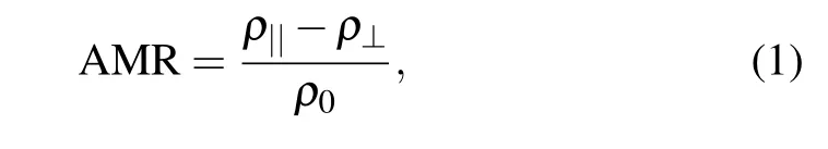
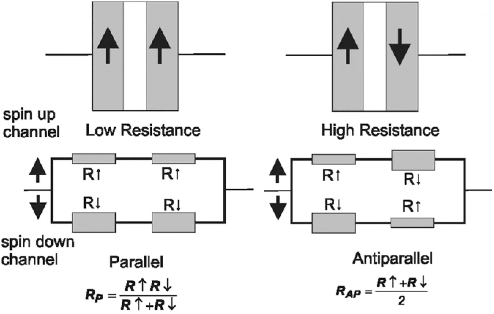
Fig.1.Schematic of Mott’s model.[6]
In Mott’s model,electrons with different spin orientations are transported in parallel through two independent channels.In an Fe/Cr/Fe three-layer structure,when the magnetic moments in the two FM layers are arranged in parallel,the total resistance of the system isHowever,when the magnetic moments in the two FM layers are arranged to be antiparallel,the total resistance of the system isHere,R↑and R↓represent the resistance of the spin-up and spin-down electrons,respectively.The GMR effect is defined as follows
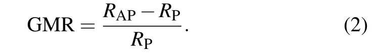
The GMR effect is substantially larger in magnitude than AMR.In terms of information storage,this feature of GMR can greatly improve the storage density and storage stability of a disk.The GMR effect suggests a new physical concept,i.e.,spin-related transport.In 1991,Dieny et al.[7]experimented with the use of a Cu layer to separate two FeNi layers and utilize the exchange-bias effect between the FM and antiferromagnetic metal(AFM)layers.This structure is also called a spin valve,as shown in Fig.2.[8]In the spin-valve configuration,the appearance of the GMR effect can be realized in a low field.
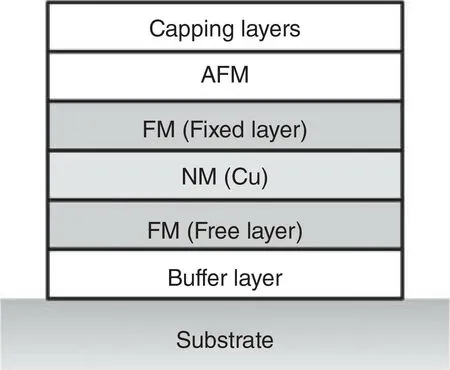
Fig.2.Spin-valve structure.[8]
When the metal layer in a GMR film structure is replaced by an insulating layer,tunneling can occur.The magnetoresistance effect in this structure is called tunnelling magnetoresistance(TMR).In 1975,Juliere et al.[9]first discovered the TMR effect in the three-layer structure Fe/Ge/Fe,and they proposed the physical mechanism of TMR,[10]which is different from that of GMR.A magnetic tunneling junction(MTJ)with the TMR effect exhibits a larger magnetoresistance ratio,higher sensitivity,and lower power consumption,[11]which thus increases concerns about spintronics.
1.2.Spin-polarized currents and spin-transfer torques
The application of GMR and TMR has greatly improved recording density in hard disks.However,information writing still needs to be performed by the mechanical movement of a coil or of the magnetic recording material.This process not only greatly reduces the writing speed but also consumes high power.Furthermore,the appearance of the spin-transfer torque(STT)produced by a spin-polarized current indicates that the magnetic moment can be manipulated by an electrical current or by the direct transfer of spin angular momentum,which enables the manipulation of nanoscale magnetic devices without nonlocal magnetic fields.
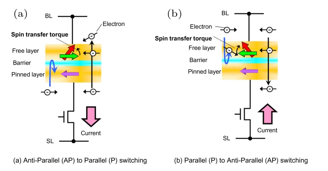
Fig.3. (a)Antiparallel to parallel switching. (b)Parallel to antiparallel switching.[15]
Spin polarization refers to the fact that the net spin of the current carriers is not zero;that is,the number of conducting electrons with different spin orientations is different.For example,in transition metals,when scattering occurs between 4s electrons and 3d electrons at the Fermi surface,the number of electrons with opposite spin orientations is unequal such that a spin-polarized charge current occurs.The STT effect first appeared in the late 1970s. Berger[12]first experimentally found that an electric current can drive domain-wall movement. Later,Slonczewski[13]and Berger et al.[14]independently proposed STT,which can be explained as follows:when a charge current passes through a magnetic material,the electrons in the charge current undergo spin polarization and then enter another layer of the magnetic material.At this point,angular-momentum transfer occurs between the spin carried by the electrons and the local magnetic moment in the magnetic material,and this interaction changes the state of the magnetic moment.The process of STT-induced magneticmoment switching is shown in Fig.3.Recently,devices that use STT for writing information have been developed and are gradually being commercialized.
1.3.Pure spin currents and spin–orbit torques
Although the STT effect produced a huge breakthrough in storage technology,there remain many challenging problems.When writing information using a spin-polarized current,the magnetic moment is partially reversed if the current is not sufficiently large,and the information is then written incorrectly.Conversely,when the current is too large,the potential barrier is broken down.Therefore,it is difficult to manufacture largescale memories in which enough spin current can pass through the tunnel barriers to drive reliable magnetic switching without occasionally damaging a barrier.Achieving reliable reading of the MTJ resistance without causing switching is also a challenge. The subsequently discovered spin–orbit torque(SOT)can be used to overcome the difficulties encountered in the application of the STT effect.
In a FM/heavy metal(HM)bilayer structure,when a charge current is introduced into the HM layer,a pure spin current is generated by the strong SOC in the HM layer.This pure spin current can generate a torque on the magnetization in the adjacent FM layer.Since this torque is derived from the SOC action in the material,it is called SOT.Unlike STT,the SOT carrier is a pure spin current rather than charge current.
In 2012,Liu et al.[16]reported the giant spin Hall effect(SHE,to be discussed later)in the high-resistivity form of tantalum(β-Ta),which allows an electrical current in a thin Ta layer to induce efficient SOT switching of an adjacent thin FM film for both perpendicular-to-plane and in-plane magnetic-anisotropic devices at room temperature.As shown in Fig.4(a),the in-plane three-terminal device comprises the multilayer Ta/CoFeB/MgO/CoFeB/Ta/Ru,where the thin layer of MgO(1.6 nm)is used as a tunnel barrier between the thin CoFeB free layer(1.6 nm)and the thicker CoFeB reference layer(3.8 nm).This allows the TMR effect to be used to determine the relative orientation of the layer magnetizations.The authors applied a DC current ITato the Ta microstrip while monitoring the differential resistance dV/dI of the structure with a relatively small current.As shown in Fig.4(b),when ITais swept,abrupt hysteretic switching of the MTJ resistance occurs,which results in antiparallel to parallel(AP to P)switching,and this switching is reversed(P to AP switching)when the current is swept back.With such improvements,a lower writing current can reduce power consumption,making reading and writing faster,while providing the added advantage of separation between the low-impedance switching(the writing process)and high-impedance sensing(the reading process).This separation solves the reliability challenges that presently limit applications based on conventional twoterminal MTJs,while also yielding improved output signals.In addition,SOT can be used to drive the movement of magnetic domains,which has great application prospects in track storage.
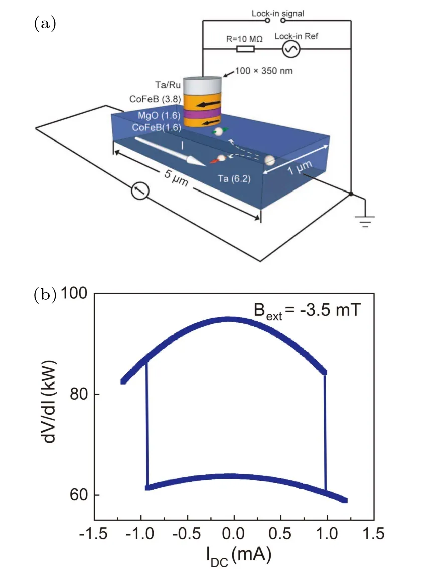
Fig.4.SHE-induced switching for an in-plane magnetized nanomagnet at room temperature. (a)Schematic of a three-terminal SHE device and the circuit for measurements.(b)TMR of the device as a function of the applied DC current IDC.[16]
2.Spin currents and spin–orbit torques
2.1.Spin-orbit coupling
Spin-orbit coupling(SOC)is a relativistic effect in which the spin polarization and magnetic moment of an electron are linked.When the electrons move in an electric field,an effective magnetic field Bis generated:
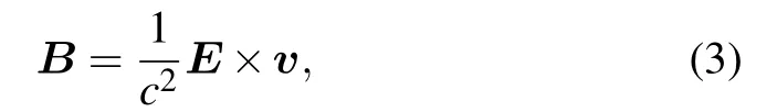
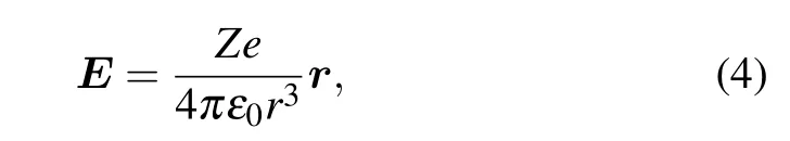
where c is the speed of light,and υ is the velocity of the electrons.When an electron moves around a nucleus,the electric field is given by the following equation:

The spin magnetic moment resulting from the spin angular momentumcan be calculated as follows:
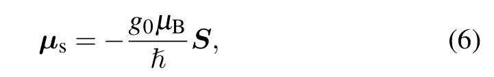
and using Eq.(6),the SOC Hamiltonian of the electron can be written as follows:
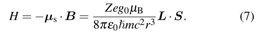
In an actual material,the energy-band structure of the material greatly influences the SOC effect,which is generally proportional to Z4.[17]This suggests that the SOC is larger for atoms that are further down a particular column of the periodic table(such as Pt,Ta,and W).
Depending on the nature of the symmetry breaking,different types of SOC effects have been observed in solids,including the Dresselhaus effect and the Rashba effect. The Dresselhaus SOC originates from the inversion-symmetry breakdown of bulk materials(such as GaAs and InSb),and the Hamiltonian of the electron can be expressed as follows:[18]
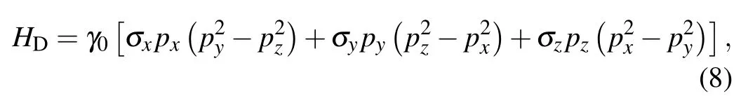
where γ0is the gyromagnetic ratio,is the vector of the Pauli spin matrices,andis the momentum of the electron. In a two-dimensional electron gas(2DEG),the z-direction component of the momentum is quantized;therefore,the Hamiltonian can be written as follows:

The Rashba SOC is derived from the interface between materials or the inversion of symmetry at a material-surface structure.[19]In 1984,Rashba and Bychkov used SOC to explain the behavior of the electron spin in a two-dimensional semiconductor structure.[20]At the interface of a semiconductor heterojunction,the energy-band structure is asymmetric,with a potential difference at the interface.Therefore,a strong built-in internal electric fieldexists at the interface,which leads to the appearance of SOC.In this case,the Hamiltonian can be written as follows:
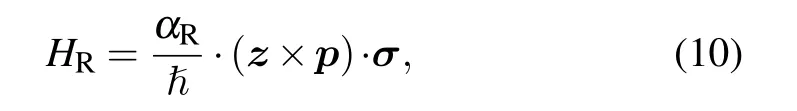
where αRis the Rashba parameter. Furthermore,a strong Rashba SOC has been found in some new materials,[20]such as the interface between graphene and metal and the surface of a topological insulator(Bi2Se3).The exploration of Rashba SOC is at the core of the research areas in spintronic electronics.
2.2.Expression for a pure spin current
There are two types of transport carriers for a spin current,namely,electrons and magnons.[8]
2.2.1.Electron-based spin current
We know that electrons carry both charge and spin;therefore,the presence of a charge current means the presence of a current of spin.The driving force for a current in this system is the gradient of the electrochemical potential:[8]
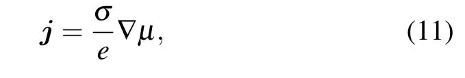
where σ is the conductivity,e is the elemental charge,andµis the electrochemical potential.After taking spin into account,the electrochemical potential iswhereoris the direction of spin polarization,is the chemical potential for theorspins,and φ is the electrical potential difference.Therefore,the current density including the spin can be expressed as follows:
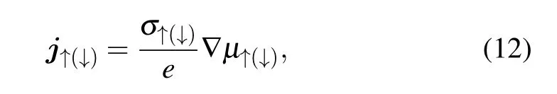
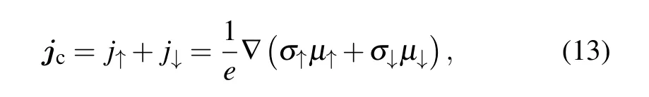
and the spin current is
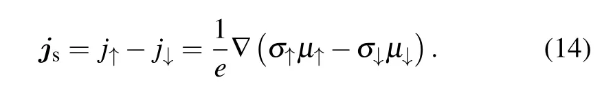
The continuity equations for charge current and spin current are as follows:
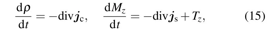
where ρ is the charge density,is the z-component of the magnetization(z is defined as the axis of quantization),and Tzrepresents a spin-relaxation term.
In equilibrium,we have
Therefore,
Equation(17)is the charge-diffusion equation and equation(18)is the spin-diffusion equation,whereis the spin-diffusion length,D is the spin-diffusion coefficient,and τsfis the spin relaxation time
where the coefficients A,B,C,and D can be determined by using boundary conditions. This derivation shows that the unequal electrochemical potentials of electrons with different spin orientations are the origin of the spin current.The reason for the unequal electrochemical potentials lies in the strong SOC inside the material(or the strong SOC at an interface,caused by the different Fermi energies of the two materials).
Let us consider nonlocal spin-valve experiments as an example to illustrate electron-based spin transportation. In 2006,Valenzuela and Tinkham[21]used nonlocal electrical methods to generate and detect spin currents. As shown in Fig.5(a),a thin aluminum(Al)Hall cross is oxidized and contacted by two ferromagnetic electrodes having different widths(FM1 and FM2).In this structure,one ferromagnetic electrode(FM1)is used to inject spin-polarized electrons via a tunnel barrier in one of the arms of the Al Hall cross. The spinpolarized current produces unequal electrochemical potentials for the spin-up and spin-down populations in the Al,and a spin current flows to both sides of the contact and decays over the spin-diffusion length λsf.Since the current is driven away from the Hall cross,only a pure spin current flows as a result of the spin injection.Because of the inverse spin Hall effect(ISHE),the spin current induces a transverse charge imbalance and generates a measurable Hall voltageVSH.Moreover,a spin imbalance occurs in the Al film,with a spin direction defined by the magnetization orientation of the FM electrode.Therefore,as shown in Fig.5(c),the spin Hall resistance,defined as RSH=VSH/I,is expected to vary when a magnetic field B⊥is applied perpendicular to the substrate.Therefore,electrical methods can be used to detect a pure spin current.
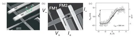
Fig.5.(a)Device fabricated with CoFe electrodes(light gray)and an Al channel(dark gray).(b)A representative measurement configuration.(c)Typical ISHE signals.[21]
2.2.2.Spin currents supported by magnons
In magnetic materials,the precession of the magnetic moment can stimulate the generation of a spin wave with magnons as the elementary excitations,as shown in Fig.6.and they can be used as the carriers of a spin current to realize spin transport. In general,a spin current can only be transported in magnetic insulators as a spin wave.When a magnon is used as the carrier for transport,it is not accompanied by the transfer of charge;therefore,the magnon spin current does not generate Joule heat.The magnon spin current can also exert a torque on the magnetic moment in the magnetic material,so it can be used to control the magnetic moment.
We take the experiments done by Wu Hao(who graduated from Lanzhou University and currently at the Institute of Physics,the Chinese Academy of Sciences)et al.at the Institute of Physics of the Chinese Academy of Sciences as an example to illustrate magnon-based spin transportation.[22]They focused on vertical spin transportation through a Pt/YIG/Pt sandwich structure(YIG is a ferrimagnetic insulator with very low Gilbert damping),as shown in Fig.7(a).When an electric current is supplied to the bottom Pt layer,it induces a pure spin current due to the SHE;moreover,it can propagate through the YIG in the form of magnons and be detected at the upper Pt layer as an electrical signal because of ISHE.Angularmomentum conservation demands that the induced magnons have their angular momenta in the y-direction,and the voltage signal always scales with the square of the y-component of the magnetization,as in the data shown in Fig.7(c). A control sample,in which one of the Pt layers is replaced by Cu,does not show such properties but only exhibits possible Joule heating and the resulting spin Seebeck effect(SSE).This result provides a direct and clear demonstration that quasiparticle magnons can efficiently serve as spin information carriers for spin-based storage and processing applications.
Note that the propagation length of the conductionelectron spin current in a metal is generally in the range of 1–1000 nm,while the propagation length of the magnons is generally large,in some cases even up to a millimeter,in materials with very low Gilbert damping.[23]
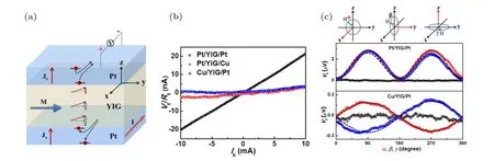
Fig.7.(a)The proposed spin-transport processes in a Pt/YIG/Pt structure.The spin current is generated by the charge current in the bottom Pt layer via the SHE,resulting in spin accumulation at the bottom Pt/YIG interface.Subsequently,the magnon current excited by the spin accumulation diffuses from the bottom to the top interface,where it converts back to an electron spin current in the top Pt layer.Finally,the spin current in the top Pt layer is detected by the voltage produced via the ISHE.(b)The Vt/Rt–Ib characteristics measured in Pt/YIG/Pt,Cu/YIG/Pt,and Pt/YIG/Cu samples.(c)The definition of the angular variables α,β,and γ used in this figure.A 3 kOe magnetic field of constant magnitude is applied to saturate the magnetic moment M during sample rotation.The lower panels show the magnetization-direction dependence of the magnon-drag voltage in Pt/YIG/Pt and of the spin Seebeck voltage in Cu/YIG/Pt.[22]
2.3.The spin Hall effect and interfacial Rashba–Edelstein effect
The application of the SOC effect produces a pure spin current,while the spin Hall effect(SHE)and the interfacial Rashba–Edelstein effect are two important SOC phenomena that produce spin currents.
2.3.1.The SHE and inverse SHE
2.3.1.1.The SHE
As early as 1971,to generate a pure spin current,Perel and Dyakonov[24]proposed using the SHE in a nonmagnetic material(NM),based on the idea of asymmetric Mott scattering.[25]This so-called extrinsic SHE remained unexplored until recent proposals that put forward a similar prediction[26,27]as well as the possibility of a strong intrinsic SHE.[28]
The SHE has gained a distinct place since its first observation a decade ago.[29,30]In the direct SHE,an electrical current passing through a material with strong SOC can generate a transverse pure-spin current polarized perpendicular to the plane defined by the charge and spin currents.The bulk SOC generally originates from the energy-band structure or from impurity scattering. Moreover,it can lead to the asymmetric scattering of electron spins,which makes the upward-and downward-spin electrons move in opposite directions(Fig.8).
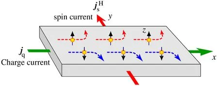
Fig.8.Spin current generated by the SHE.[31]
When a charge current is injected into a HM layer,a transverse spin current is produced. The expression for the spin current generated by the SHE is as follows:
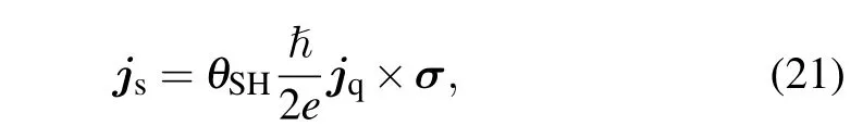
where θSHis the spin Hall angle(SHA),which represents the conversion efficiency between the spin current and the charge current in the material.Here,is Planck’s constant divided byis the charge current,andis the spin-polarization direction of the electron.
Generally,the SHE has the same physical origin as the anomalous Hall effect(AHE).[32]The spin-dependent Hall effects(AHE,SHE,and ISHE)originate from three distinct microscopic mechanisms that they all share:the skew,the side jump,and the intrinsic mechanisms. These mechanisms are caused by coherent band-mixing effects induced by the external electric field and the disorder potential,and this makes them more complex than the simpler single-band effects.
Skew scattering is caused by chiral features that appear in disorder scattering in the presence of SOC.This mechanism was first identified in FMs by Smit[33]and has its origins in Mott scattering in relativistic physics:[25]In the presence of SOC,either in the Hamiltonian of a perfect crystal or in the disorder Hamiltonian,a transition that is right handed with respect to the magnetization direction has a different probability than the corresponding left-handed transition.In simple models,the asymmetric chiral contribution to the transition probability of momentais often assumed to have the form

Inserting this asymmetry into the Boltzmann equation leads to a current proportional to the longitudinal current driven by the electric fieldand perpendicular to bothand,whereis the magnetization direction in case of the AHE and is the direction of polarization of the spin current in case of the SHE.The corresponding contribution to the Hall conductivity is proportional to the transport lifetime τ.
The side-jump mechanism was first noticed,but discarded,by Smit.[33]It was reintroduced by Berger,[34]who argued that it was the key contribution to the AHE.It is important to remember that there are always two sources of sidejump scattering:
(1)Extrinsic side jump:This is the contribution arising from the spin–orbit coupled part of the wave-packet scattering off the spin–orbit coupled disorder.
(2)Intrinsic side jump:This is the contribution arising from the spin–orbit coupled part of the wave packet formed by the Bloch electrons scattering off the scalar potential alone without SOC.
The two mechanisms are independent of each other,but depending on the crystalline environment and the type of scattering impurity both can be important.[35]
The intrinsic contribution to the spin Hall conductivity depends only on the band structure of the perfect crystal.There is a direct link of the intrinsic effect to semiclassical theory,in which the induced inter-band coherence is captured by an anomalous velocity arising from a momentum-space Berry phase,which was described by Murakami,Nagaosa,and Zhang et al.[27]
Dyakonov and Perel[24]first proposed a phenomenological theoretical explanation for the SHE.They derived the diffusion equation for the spin current from the electron-diffusion equation,which can be written as follows:
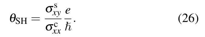
As this shows,θSHis determined by the substance itself(that is,it is an intrinsic physical quantity).Therefore,to improve the efficiency of the generation of a spin current,materials with a large SHA can be selected as the source of the spin current.Recently,researchers have found that heavy metals,topological insulator surfaces,2DEGs,and other materials possess a relatively large SHA.[32]
Here,we introduce an experiment to access the SHA experimentally. Chen Caigan(Fudan university)et al. used an H-shaped structure to measure the θSHof monolayer Au metal,[36]as shown in Fig.9.This method measures the θSHof Au using pure electrical transport without using any magnetic materials.
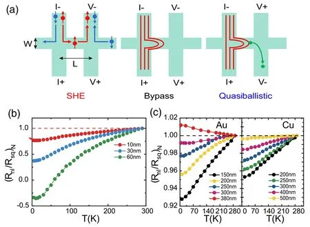
Fig.9. Detection of the SHA of Au with an H-shaped structure. (a)A schematic of the three mechanisms in the H-shaped measurement:the SHE,the bypass effect,and the quasi-ballistic effect.(b)The(Rnl/Rsq)N versus T curve for Au films of different thicknesses.(c)The(Rnl/Rsq)N versus T curves for a 10 nm Au film and 10 nm Cu film with different widths W.[36]
In the H-shaped nonlocal measurement,there are generally three kinds of effects that dominate:the SHE,the bypass effect,and the quasi-ballistic effect,and the resistance generated by the different effects varies with the temperature.Using this feature,the nonlocal resistance generated by the SHE can be determined,and the SHA can be obtained.The resistance caused by the SHE is expressed as follows:
where Rsqis the cube resistance and W and L are geometric parameters shown in Fig.9(a). As the temperature decreases,increases with increasing spin-diffusion lengthcaused by the bypass effect remains unchanged,andcaused by ballistic transport decreases.Therefore,at low temperatures,the main source of the nonlocal resistance in a sample with a small thickness and large width is the SHE,and the θSHof Au can be obtained by measuring the resistance.For Au at 5 K,θSH=0.1,which is already very large.Furthermore,the addition of Bi(with a large θSH)to Cu(with a large λs)can yield a large θSHand a large λs.Using the same method,the SHA in a Cu(3 nm)/Bi(0.15 nm)/Cu(7 nm)structure has been measured to be θSH=0.12.
2.3.1.2.The inverse spin Hall effect
The SHE can convert a charge current into a spin current.According to the Onsager commutation relation,the inverse process of the SHE can convert a pure spin current into a charge current;it is called the inverse spin Hall effect(ISHE).The transport of a pure spin current is carried out by the transfer of angular momentum with no net charge;therefore,it is difficult to detect directly.However,the ISHE can be used to detect the spin current electrically,as shown in Fig.10.
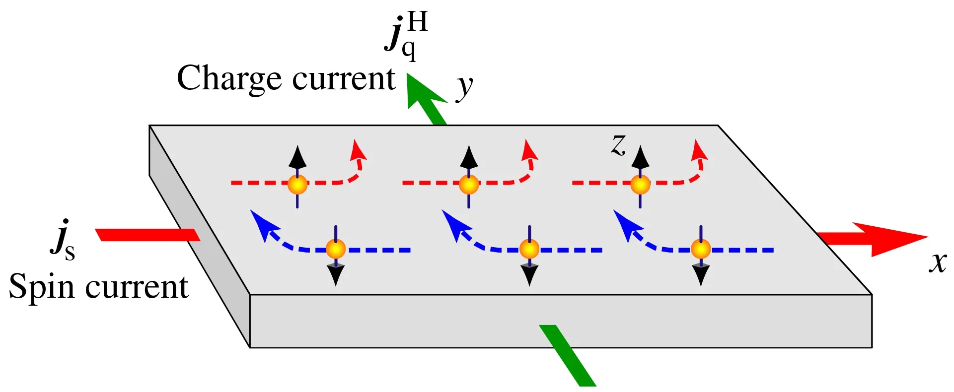
Fig.10.Schematic of the ISHE.[31]
When a spin current is introduced into a sample with a strong SOC,electrons with different spin orientations are scattered by SOC as they move,and the scattering makes the electrons move in the same direction;i.e.,the directional movement of the electrons forms a charge current
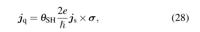
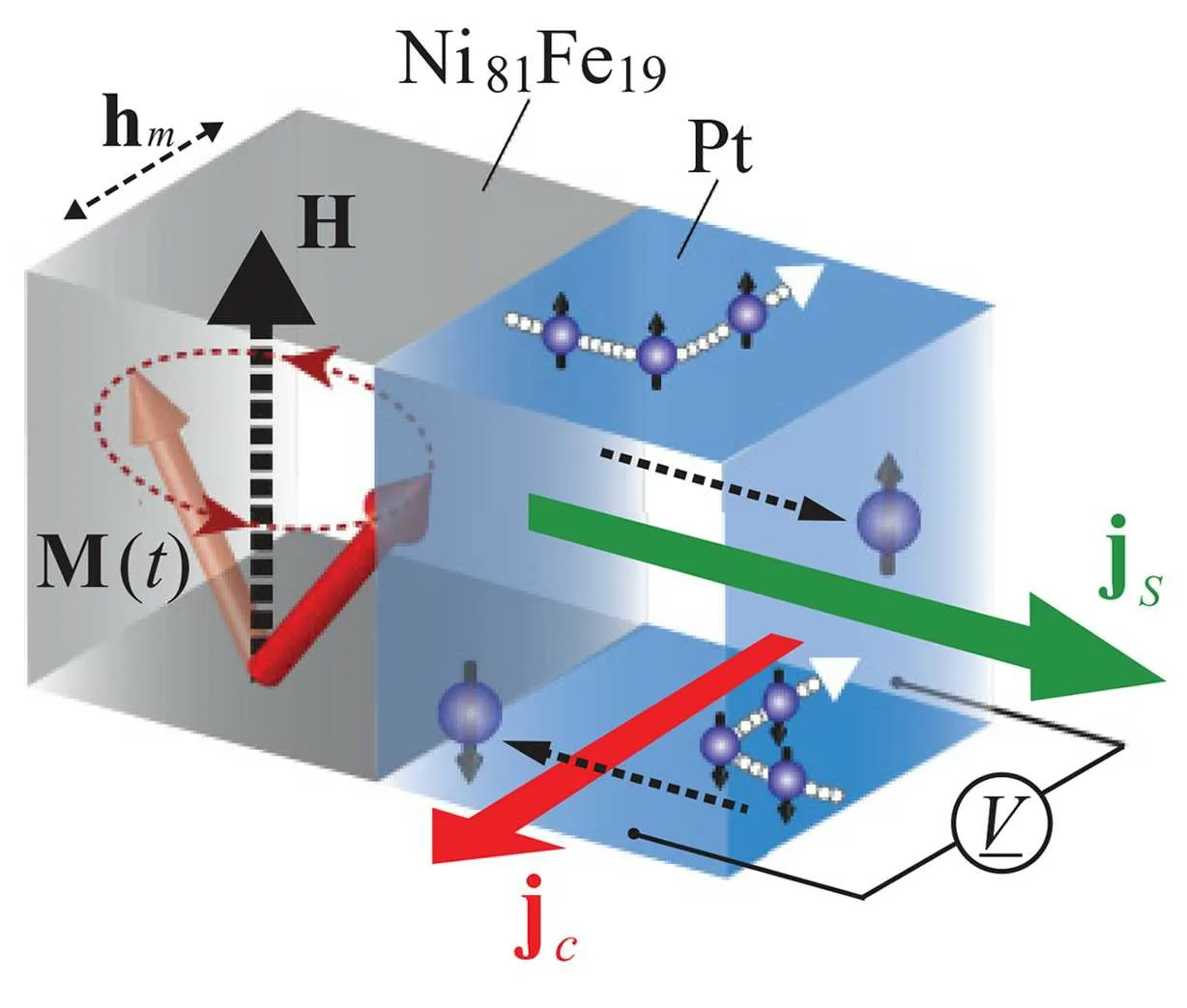
Fig.11.Detection of the spin-pumping signal in a Py/Pt structure using the inverse SHE.[37]
2.3.2.Rashba–Edelstein SOC and the inverse Rashba–Edelstein effect
As can be seen from the above experiments,the SHE provides a method of generating pure spin currents in nonmagnetic materials using electrical methods.In recent years,experiments have discovered that the Rashba SOC can generate a relatively large spin current.The Rashba effect at an interface is shown in Fig.12(a).The inverse Rashba–Edelstein effect is also known as the spin galvanic effect(SGE),as shown in Fig.12(b). This effect was explored earlier in inversionasymmetric NMs.[43]The term SGE is derived from analogy to the galvanic(voltaic)cell.SGE was initially observed in an asymmetrically confined 2DEG in a GaAs quantum well.[44]
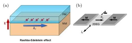
Fig.12. (a)The Rashba–Edelstein effect.[45](b)The spin galvanic effect.[44]
The charge current generated by the spin galvanic effect can be expressed as follows:

and the spin density produced by the Rashba effect can be expressed as follows:

In fact,since the intensity αRis related to the potential difference at the interface,Rashba SOC can be controlled by adjusting the potential difference to achieve adjustment of the spin current.The first spintronic concept using Rashba SOC was the spin field-effect transistor.[46]
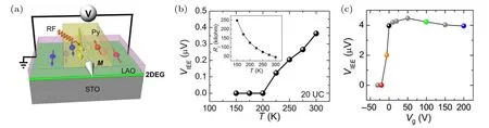
Fig.13.(a)Schematic of the IEE measurements.The spin current is injected via spin pumping from Py under a resonance condition.A voltage meter is used to probe the electric field generated by the IEE of the Rashba-split 2DEG between two insulating oxides,i.e.,SrTiO3 and LaAlO3.(b)The temperature and(c)gate-voltage dependences of VIEE of the 2DEG SrTiO3/LaAlO3.[47]
To explain the Rashba SOC effect,we consider a simple illustration based on recent experiments in the 2DEG and twodimensional transition-metal dichalcogenides(TMDs),which are typical systems with Rashba SOC.Song Qi(Peking University)et al.[47]reported observations of the inverse Edelstein effect(IEE)in the Rashba-split 2DEG between two insulating oxides,SrTiO3and LaAlO3,up to room temperature.As shown in Fig.13(a),they generated the spin current in the 2DEG by spin pumping from a ferromagnetic Ni80Fe20(Py)electrode through a LaAlO3layer. The spin-to-charge conversion of the injected spin current produced by the Rashba SOC created an electrical voltage(VIEE).The experimental results demonstrate that the spin voltage in a Rashba-split 2DEG between SrTiO3and 3-unit cell LaAlO3can be switched on and off using a perpendicular electric field.Furthermore,VIEEquickly decreases as the temperature decreases,and it is no longer detectable below 200 K[Fig.13(b)].However,there are no existing mechanisms that can fully explain the temperature dependence of VIEE.At room temperature,the gate voltage provides a powerful tool to tune the spin-to-charge conversion efficiency[Fig.13(c)].The key result in these experiments is that they demonstrate that the Rashba-split 2DEG at the complex oxide interface can be used for efficient chargeand-spin conversion at room temperature to generate and detect spin currents.
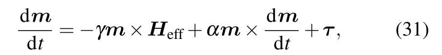
Yao Qunfang(East China Normal University)et al.studied the Rashba SOC of WSeTe(a kind of TMD)using density functional theory calculations.[48]As shown in Fig.14(b),they found that the intrinsic out-of-plane electric field generated by the broken mirror symmetry of the structure leads to a large Rashba spin splitting,which can be tuned easily by applying an in-plane biaxial strain.In addition,they calculated the influence of the external electric field on Rashba SOC and found it to be less effective than strain.Moreover,they found that the Rashba parameter αRof the TMD increases linearly with the electric field[Fig.14(a)].
These experimental and theoretical results show that the strength of Rashba SOC has a great influence on the spin current.The efficiency of spin-current generation can therefore be improved by looking for materials with a strong SOC effect(or by adjusting the interfacial structures of materials).
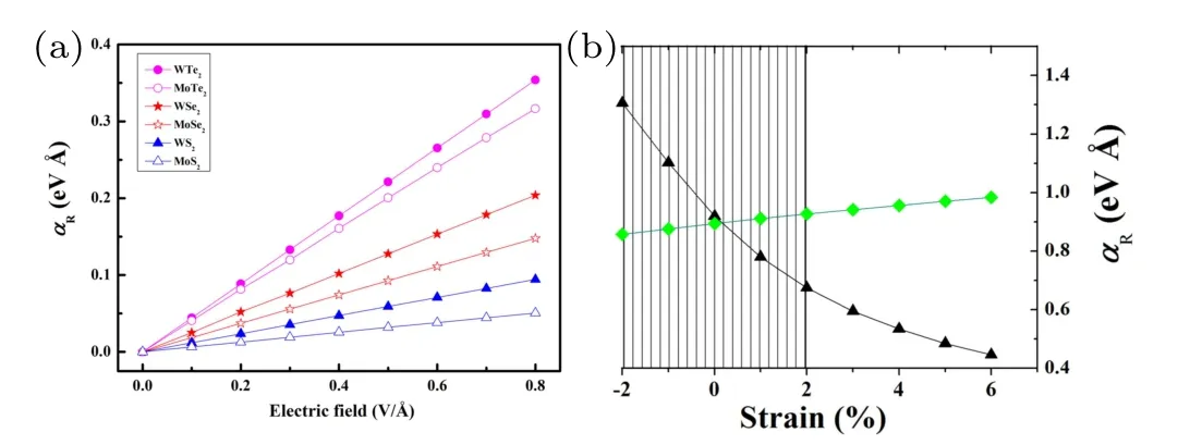
Fig.14.(a)The electric-field dependence of the linear Rashba parameters of six MX2 monolayers.(b)The Rashba parameter αR for different biaxial strains(triangles)and external electric fields(diamonds).[48]
2.4.SOT
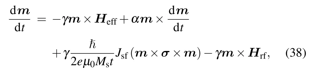
Spin-orbit torques are a current research hot spot in spintronics.Current manipulation of the magnetization via SOT was first discovered in 2009 by Chernyshov et al.[49]in an FM/HM double structure by injecting a charge current into the HM.The SOC in an HM produces a pure spin current that diffuses into the adjacent FM and generates a torque on the magnetic moment in the FM,thus changing the state of the magnetic moment.The dynamics of magnetization in an external field can be described by the Landau–Liftshitz–Gilbert(LLG)equation
where γ is the gyromagnetic ratio,is the unite magnetization,is the effective magnetic field,α is the Gilbert damping factor,andis the SOT.The first term on the right side of the equation represents the precession of the magnetic moment around the effective magnetic field;the second term represents the damping precession of the magnetic moment;and the third term is the torque exerted by the spin current on the magnetic moment.[50]This torque can be decomposed into two parts:a field-like torqueand a dampinglike torque
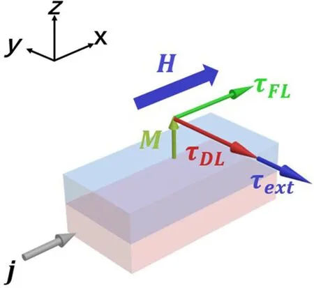
Fig.15.The SOT acting on a magnetic moment is decomposed into two mutually perpendicular torques.[51]
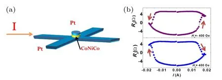
Fig.16.Using the spin–orbit torque to switch the magnetic moment in CoNiCo.(a)The structure of the device.(b)The current-switching loop under an in-plane field of±400 Oe in the x-direction,where the arrows indicate the loop directions.[52]
Furthermore,the SOT effect can be used to drive domainwall(DW)movement.Experimentally,it has been observed that the inclusion of relativistic torques leads to a large increase of domain-wall velocities for optimally tuned materials,which is potentially of technological interest.In an experiment by Emori,[54]the spin current is generated by the SHE of Pt and Ta,and the SOT effect is used to drive the motions of domain walls in the Pt/CoFe/MgO and Ta/CoFe/MgO structures,as the data shown in Fig.17.
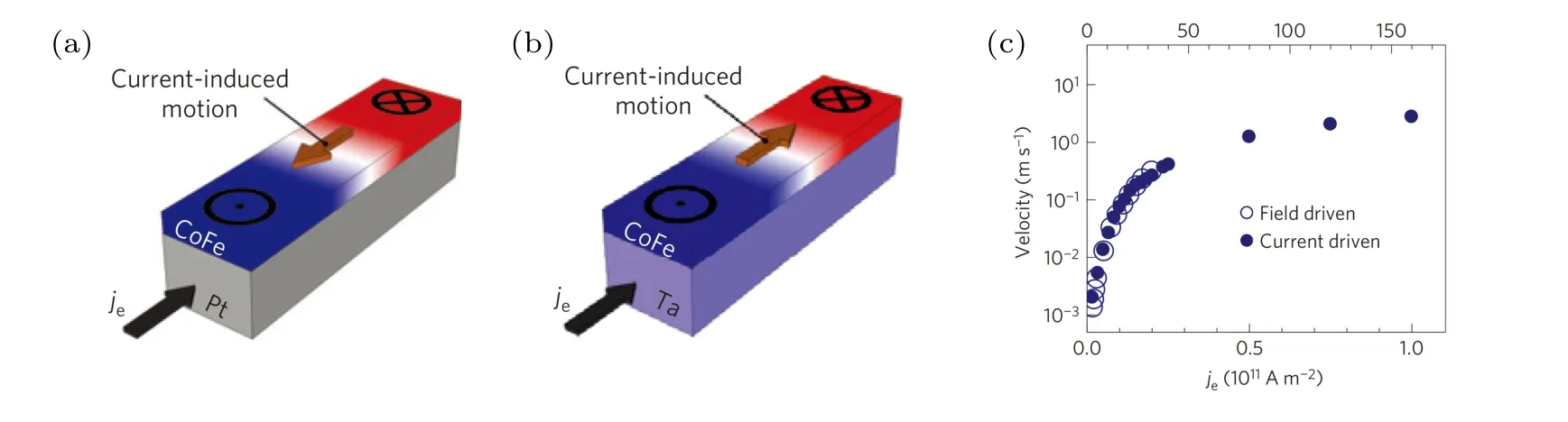
Fig.17.Using spin–orbit torques to drive the motion of domain walls.(a)Illustrations of the direction of current-driven DW motion in Pt/CoFe/MgO and(b)Ta/CoFe/MgO.(c)The DW velocity as a function of je.[54]
For films with perpendicular magnetic anisotropy(PMA),magnetization can be switched by SOTs in a fixed in-plane applied magnetic field;without a magnetic field,switching is in a random up or down direction. However,the requirement for an external magnetic field greatly limits the applications of SOT.Therefore,a large volume of work has focused on magnetization switching by SOTs without external fields.The use of an SOT-driven magnetic-moment switch is thus required to solve the main problems in improving efficiency and achieving a field-free switch.
3.Physical effects associated with pure spin currents
3.1.Spin pumping
Spin pumping(SP)is a fundamental approach for generating pure spin currents. The precessing spins in an FM act as peristaltic pumps,adiabatically injecting spins out of the FM layer into the adjacent HM layer without charge transport.[55]Therefore,SP can be understood as the inverse of SOT,and it provides access to the physics of spin dynamics,damping,and spin currents.[56]In the last few years,experiments on SP have been extended from magnetic metals to magnetic insulators,[57]topological insulators,[58,59]and AFMs/oxides,[60]and have presented more and more interesting features of this novel effect.
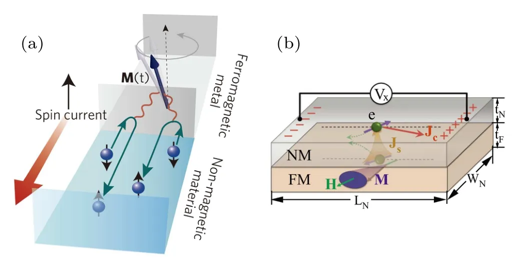
Fig.18.(a)Illustration of SP spin-current generation from an FM into an HM by means of magnetization dynamics.[61](b)Schematic of the ISHE induced by spin pumping in an FM/HM bilayer system.[62]
This phenomenon was observed experimentally in the early 2000s.[63]The experiments showed enhanced Gilbert damping in FMR measurements associated with the loss of angular momentum due to a spin current flowing from the FM into the HM.In this setup,the HM served as a spin sink.The precessing magnetization in the FM generates a timedependent spin current at the FM–HM interface that flows into the HM.The DC component of the spin-current densitythrough the interface is given by
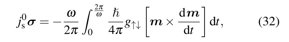
where σ is the polarization direction,is the unit vector of magnetization,is the real part of the spin-mixing conductance,andis Planck’s constant divided byNote that the direction of the pumped spin current is determined by the bilayer geometry,i.e.,it is along the interface normal from FM to HM,and the spin polarization is opposite to that of the equilibrium magnetization in the FM layer.Equation(32)shows that thehas the same form as the Gilbert-damping term in the LLG equation.Therefore,the damping enhancement in early studies of SP is given by the following equation:
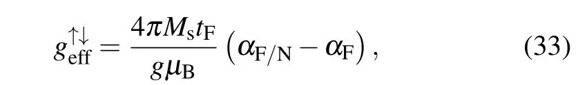
This is a key parameter for SP,which represents the efficiency of spin-current generation by SP.Here,g is the Landé factor;µBis the Bohr magneton;αF/Nis the damping factor of the FM/HM structure;αFis the damping factor of FM;Msis the saturation magnetization;and tFis the FM thickness.We would like to highlight the importance of Eq.(33),since it is the only method for experimentally determiningwhich is a key parameter that includes the details of the spin current flowing across the FM/HM interface.It has been widely related to the quantitative analyses of the experimental data on spin Hall magnetoresistance,spin torque FMR,SP,and even the interfacial Dyzaloshinskii–Moriya interaction(DMI).[65]
The detection of the pure spin current flowing into the HM can be electrically performed via the ISHE,as was demonstrated by Saitoh et al.in 2006.[66]Because of spin relaxation and diffusion in normal metals,the spin-current density decays exponentially along the flow direction.This can be calculated by solving the spin-diffusion equation subject to appropriate boundary conditions:

where z is the transmission distance of the spin current in the HM,is the spin current generated at the FM/HM interface,λsdis the spin-diffusion length,and tNis the thickness of the HM layer.The SOC in the HM layer allows the transformation of the spin currentinto the charge currentvia the ISHE,which was demonstrated by Saitoh,[66]
After integrating the charge current along the z-axis(in the thickness direction),the effective charge current because of the ISHE associated with SP is given by the following equation:
Because this gives the voltage signal that is usually detected in experiments,we define x as the orientation of the electrodes. The detectable voltage signal is given by Vx=where LNand σNare the length and conductivity of the HM,respectively.From Eq.(36),the voltage signal because of SP is given by the following equation:
In collaboration with Zhou Shiming at Tongji University,we have used heterostructure systems comprising an isoelectronic PdPt alloy and YIG and have investigated the mechanisms of SOC tuning on the effective spin-mixing conductance,the SHA,and the spin-diffusion length.[68]Among the various physics parameters of the PdPt alloy,only the SOC strength changes significantly with the alloy composition,as shown by the experimental results in Fig.19.We determined that the local density of states is enhanced for Pt-rich alloys,leading to aenhancement when the Pd atoms are replaced by the heavier Pt atoms.Among the three contributions to the spin Hall conductivity(SHC),the skew scattering plays the dominant role.In particular,skew scattering parameter has for the first time been observed to increase with increasing SOC strength. At the same time,the Elliott–Yafet spin-flip scattering model proves to govern the propagation of the spin current in PdPt alloys,resulting in a decrease of the spin-diffusion length(SDL)with increasing Pt concentration.
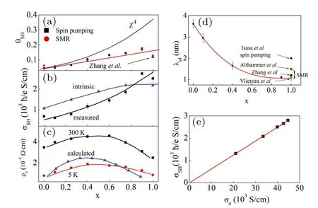
Fig.19.For PdPt(15 nm)/YIG(80 nm):(a)θSH from both SMR and spin pumping and(b)σSH at 300 K,(c)ρ at 5 and 300 K,(d)the spin-diffusion length as a function of the ratio VISHE/R versus the Pt thickness,where R is the sheet resistance of the sample strip,and(e)σSH versus the electrical conductivity σ.In(a),for comparison we also give the Z4 dependence and the data(blue up-triangles)for Pt/YIG taken from Zhang et al.,where θSH(x)=θSH(x=0)(Z/46)4 with Z=78x+46(1 −x).The intrinsic spin Hall conductivity(SHC)(blue up-triangles)(b)and the longitudinal resistivity(blue up-triangles)(c)of single-crystal PdPt alloys are also given from ab initio calculations.In(b),(d),and(e),the data were measured using SP.The solid lines serve a guide to the eye in(a),(b),and(c),and they refer to fitted results in(d)and(e).[68]
The spatial symmetry of SP,i.e.,the variation of the ISHE voltage amplitude with the orientation of the magnetization and polarization directions of the dynamic magnetic field,is a key feature of the SP effect.[69]This symmetry is quite important,because it is the only criterion for distinguishing SP from other ferromagnetic resonance(FMR)[70,71]related electrical effects;moreover,it is the foundation for discovering the physics of pure spin currents.For example,the SP signals are always tangled with spin rectification,which is a nonlinear coupling between the conducting electrons and local spins through magnetoresistance effects.[72]This problem was recently solved by Bai et al.,[70,71]who proposed a universal method for separating them in HM/FM devices,based on the differences in the spatial symmetries of SP and spin rectification.
We presented a systematic study of the spatial symmetry of the SP effect associated with the ISHE.The main symmetry of the voltage as a function of the magnetization direction is dominated by the ISHE and the effective dynamic field acting on the magnetization,which are summarized in Fig.20. The anisotropy in the resonance linewidth and the spin-mixing conductance,however,would distort the main symmetry.For the in-plane case,because these parameters are isotropic,our experimental results are consistent with theoretical predictions.For the out-of-plane case,although the basic symmetry of the experimental results is similar to the theoretical predictions,we found a significant discrepancy. This discrepancy has been demonstrated to arise both from the resonance linewidth and from the anisotropy inwhich is an open question for the SP effect.[62]
The SP experiments were mostly performed in the linear dynamic regime;specifically,a linear solution to the Landau–Lifshitz equation with a linear damping term is sufficient to describe the dynamic process and energy dissipation in an FM.However,recent interest in SP has extended from the linear to the nonlinear dynamics regime,[73,74]which is necessary for a deeper understanding of the links between SP and spin dynamics.It is known that nonlinear spin dynamics differs distinctly from the linear response,and a variety of amplitude-dependent nonlinear effects may be present.[75]In particular,this is the case for the nonlinear damping that has been found to be present and to dominate the dynamic energy/spin-moment dissipation for spin precession angles above a few degrees.[76,77]Since SP is closely related to the damping process,it is interesting to ask whether the nonlinear damping term may be involved in the SP process.We studied the SP occurring under the nonlinear spin dynamics in a Pt(17 nm)/Y3Fe5O12(YIG 66 nm)heterostructure.By using high-power excitation,the precession angle(θc)of the YIG can reach a value as high as 23◦,and distinct nonlinear dynamic effects,such as foldover ferromagnetic-resonance spectra and nonlinear damping,[77]have been observed,as shown in Figs.21(b)and 21(c).The linear relation between the DC component of the spin current and sin2θchas been tested from the linear to the nonlinear spin-dynamics regimes,which indicates that SP is a robust effect that is independent of the damping mechanism in an FM,at least under our power levels(<200 mW).

Fig.20.Spatial symmetry of the spin-pumping signal(ISHE voltage).The three rows correspond to rotation of the magnetization in the xy,yz,and xz planes.Each column corresponds to a certain device setup:The voltage can be detected either along the longitudinal direction[columns(a)to(c)]or along the transverse direction[columns(d)to(f)],where the double-headed arrows indicate the polarization direction of the dynamic magnetic field.[62]
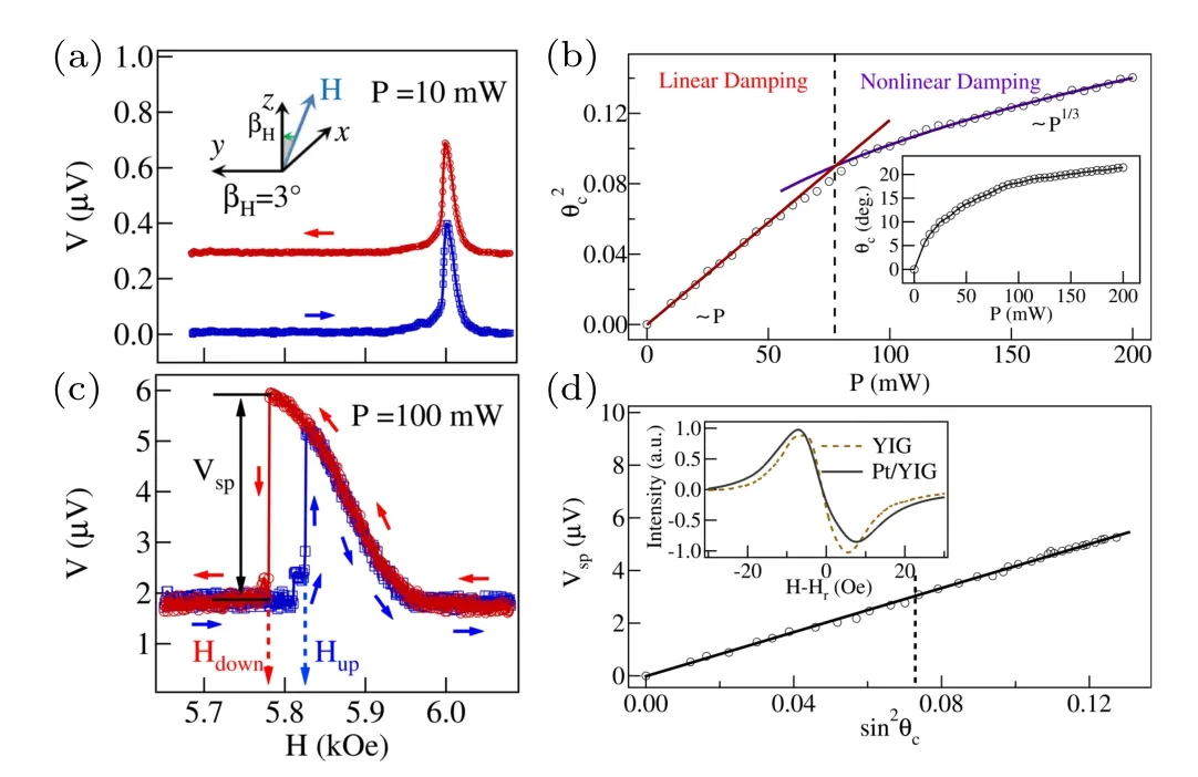
Fig.21.(a)Spin-pumping spectra of the linear FMR response with the magnetic field applied almost along the film normal,where the two curves with opposite H-sweeping directions are identical. The inset shows the direction of the applied magnetic field.(b)Foldover spin-pumping spectra under high-power excitation,where the small arrows indicate the H-sweeping direction. (c)The square of the resonance-cone angle as a function of the input microwave power,where the inset shows the power-dependent cone angle.(d)Spin-pumping voltage as a function of sin2θc.The inset shows cavity FMR spectra of YIG and Pt/YIG films.The black dotted lines are the separatrices between the linear and nonlinear regimes.[78]
Although SP has been a standard method for determining spin-related parameters such as the spin-diffusion length,spinmixing conductance,and SHA,significant inconsistencies in the reported values of those parameters exist. This problem has been addressed recently and found to be due to the underestimation of the interfacial effect. Tao Xinde(Nanjing University)et al.[79]reported a self-consistent determination of the SHA and the spin-diffusion length in Pt and Pd by considering the interfacial spin loss.As the data in Fig.22 show,one can clearly observe the different saturation tendencies of the effective spin-mixing conductance and the normalized SP signal with increasing thicknesses of the Pd deposited on different FMs.Such differences provide direct evidence of the interfacial spin loss.The authors characterized the spin-charge conversion for Pt and Pd with various FM combinations using an effective spin-mixing conductance,microwave photoresistance,and ISHE measurements,and they find that the pumped spin current suffers an interfacial spin loss,the magnitude of which varies for different interfaces. By properly treating the interfacial spin-loss effect,they obtained consistent values for Pt(θSH=0.03,λsd=8.0 nm)and Pd(θSH=0.0048,λsd=7.7 nm),regardless of which FM pumping source is used.In addition,a previously reported small spin-diffusion length is incompatible with fundamental spin-diffusion theory,in which the spin-diffusion length must be larger than the electron mean free path.The obtained value of λsdis larger than lmffor both Pt and Pd,consistent with general understanding.The approach has been demonstrated for Pt and Pd but should also be applicable to other materials.
The appearance of a symmetric resonant signal at the position of the FMR,with a sine-like in-plane angular dependence,was believed to be characteristic of the SP signal from which the ISHE could be identified. However,Wang Peng(Nanjing University)[80]experimentally showed that this state of affairs is not fundamental,but rather that one can use the unidirectional,spin-wave-propagation-induced Seebeck voltage to reproduce this characteristic without requiring either SP or the ISHE.The argument starts from the puzzle that a long spin lifetime and high spin-charge interconversion efficiency were observed to coexist in organic molecules using SP.Since organic molecules are made of elements with a weak SOC,such as hydrogen,carbon,and oxygen,for which the SOC strength is about 1–2 orders of magnitude weaker than that of the Cu atom,neither the SHE nor the ISHE is expected to be observable using regular measurement methods.Wang Peng et al.systematically investigated the DC voltage generation in a heterostructure of PEDOT:PSS[poly(3,4-ethylenedioxythiophene): poly(4-styrenesulphonate)]and a micrometer-thick YIG under FMR conditions,in which the ISHE in PEDOT:PSS was unambiguously excluded. Nevertheless,the signal still presented a sine-like angular dependence,as in the data shown in Fig.23(c).Furthermore,they found that a temperature gradient was induced by the nonreciprocal surface spin-wave propagation,with the determinant direction m×n,where n is the film normal.Moreover,both the temperature gradient and DC voltage vanished when the thickness of the YIG film was reduced to 10 nm. In addition,this unidirectional spin-wave-propagation-induced Seebeck voltage also occurred in a heterostructure consisting of a micrometer-thick YIG and a material with a large Seebeck coefficient such as graphene or a topological insulator.
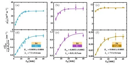
Fig.22.Extraction of the SHA and spin-diffusion length for Pd from different FM/Pd combinations.The Pd-thickness-dependent and the normalized spin-pumping signal are shown for Co16/Pd(tN),Py16/Pd(tN),and CoFe16/Pd(tN).The solid lines are fits.[79]
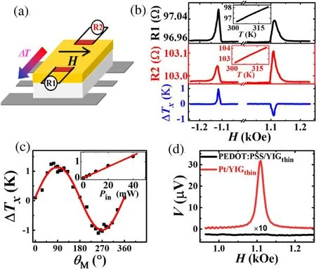
Fig.23.(a)Experimental setup for the temperature gradient measurement for PEDOT:PSS/YIG bilayer. (b)The resistance as a function of H for two thermometers R1(top panel)and R2(middle panel).The bottom panel shows ∆Tx as a function of H.(c)The θM angle-dependence of ∆Tx.The red curve is a fit to the sin θM function.The inset is the microwave-power dependence of ∆Tx,together with a linear fit(red curve).(d)The voltage signal as a function of H measured in the Pt/YIG(10 nm)and PEDOT:PSS/(10 nm)samples.[80]
3.2.Spin torque ferromagnetic resonance
Spin torque ferromagnetic resonance(ST-FMR)is an electrical detection of ferromagnetic resonance based on the effect of SOT induced by alternating current and spin rectification.The spin rectification effect indicates that the magnetic moment in a magnetic material can be precessed by a driven microwave magnetic field,thereby causing the magnetoresistance of the system to change with time.Since the microwave current also changes with time,the magnetoresistance and the microwave current are coupled together to generate a DC voltage signal,and the magnetic moment precession information can be obtained by detecting this signal.In 2011,Liu Luqiao et al.[81]proposed a method for evaluating SHA using ST-FMR technology,as shown in Fig.24.
Precession of the magnetic moments in the FM can be described by the LLG equation including SOT as follows:
where the amplitude of the symmetric voltage signal VSis related to the damping-like torque generated by SHE,and the amplitude of the antisymmetric signalVAis related to(i.e.,it is related to the current density in Pt).The ratio of the symmetric to antisymmetric components is then linked to the ratio of spin and charge currents,and thus to the SHA.
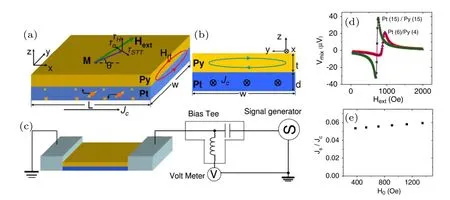
Fig.24.(a)Schematic of Pt/Py bilayer thin film illustrating the SOC induced by the SHE rising from the rf current through HM as well as the damping torque and torque due to the Oersted field when the magnetization of FM is aligned in an external magnetic field.(b)Dimensions of the sample and the Oersted field because of a current flowing through FM.(c)Electrical measurement scheme.Magnetic moment precession in a Py/Pt bilayer film detected by ST-FMR.(d)–(e)Resonance alignment obtained by ST-FMR is used to characterize the generation efficiency of the spin current.[81]
Zhang Weifeng and Han Wei(currently at Peking University)et al.,[82]using ST-FMR measurements,showed that the transparency of the Pt/FM interface to the spin current plays an important role in determining the magnitude of SHA.They found that the interface transparency T values of the Pt/Co and Pt/Py structures,which can be calculated by the following equation,are very different:
where d is the thickness of the Pt layer;λ and σPtare the spin diffusion length and the conductivity of Pt,respectively,and h is Planck’s constant.Both T andare related to the loss in spin angular momentum at the interface,which has a large influence on the value of SHA,as shown in Fig.25.
In addition to aiding in the investigation of spin-charge conversion in HM,ST-FMR is also a novel method for the study of the dynamic properties of ultra-thin magnetic films.However,because of the deterioration of AMR in ultra-thin magnetic films,the AMR-based ST-FMR would be too weak to be detected.However,an obvious AHE is expected in those films due to the considerable spin-related scattering.We propose a simple method for the electrical detection of magnetization dynamics in ultrathin films based on the dynamics of SOT and AHE.
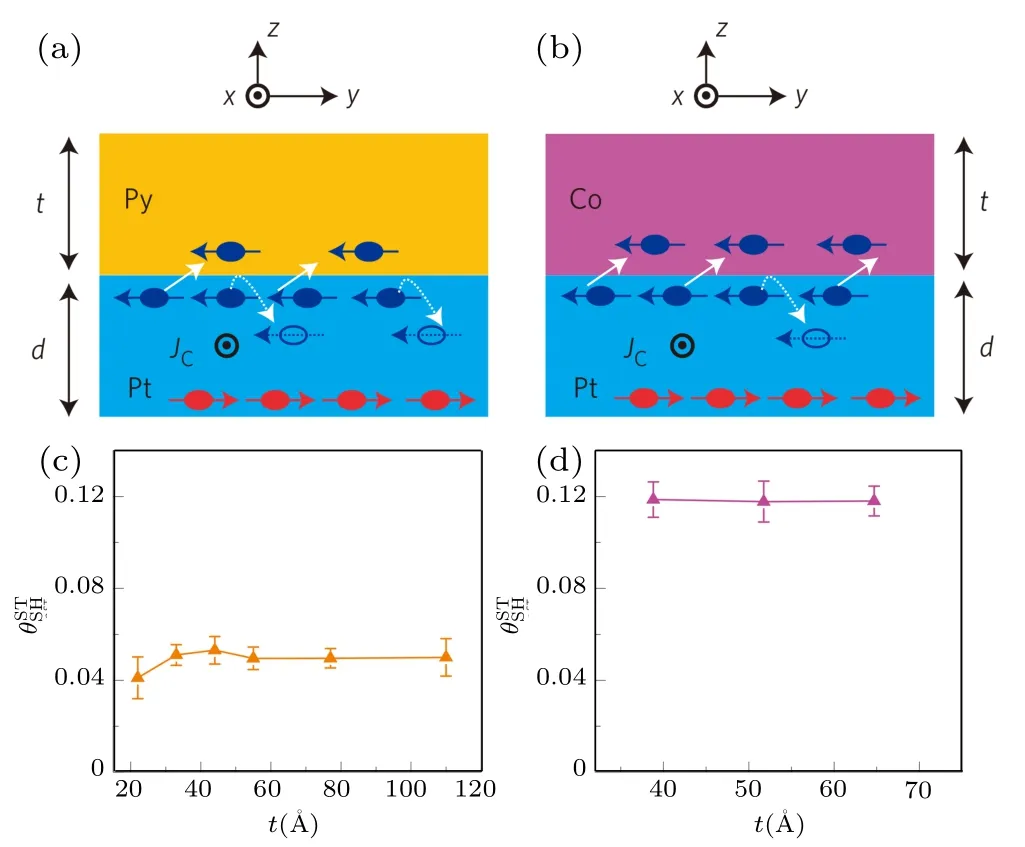
Fig.25.Schematics showing the interface transparency for(a)Pt/Py,and(b)Pt/Co.SHA of Pt as a function of FM thickness for(c)Py and(d)Co if the transparency is not considered.[82]
We took Ta/CoFeB/MgO as an example to present the results of AHE based ST-FMR as the data shows in Fig.26.Because of the interfacial nature of PMA in Ta/CoFeB/MgO,the thickness of CoFeB must be<2 nm,[83,84]which results in difficulties for transmission/reflection methods in determining the dynamic response since the signal amplitude is proportional to the sample volume.By directly sending an rf electric current into the film,the Oersted field and SHE from the adjacent Ta layer generated dynamic torques on CoFeB,and the out-of-plane component of the dynamic magnetization rectified the rf current into a resonant DC transversal voltage based on the AHE.Dynamic parameters of the film,such as gyromagnetic ratio,PMA field,and magnetic damping,can be determined.Since signal amplitude is independent of film thickness,this method is suitable for studying the dynamic properties of ultrathin magnetic films.
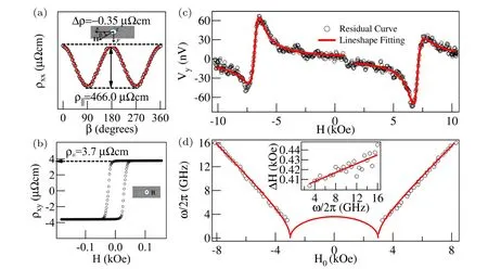
Fig.26.(a)Symbols represent longitudinal resistivity ρxx as a function of β,which is the angle between the magnetic field and the x-axis in the xy plane.Solid line is a −∆ρsin2β fit based on the principle of AMR.(b)Hall resistivity ρxy as a function of the perpendicularly applied magnetic field.(c)Symbols are data,and curves are line shape fits.(d)Dispersion curves of the resonant signals are present in Vy(H).Inset shows the FMR linewidth as a function of frequency.[85]
3.3.Spin Hall magnetoresistance
In FM/HM hybrids,the amount of spin current absorption/reflection by the FM at the FM/HM interface depends on the orientation of the FM magnetizationwith respect to the polarizationof the spin current.The amount of spin current reflected at the interface,in turn,induces a charge current via the ISHE in the HM layer.The total-orientation-dependent spin current flow across theinterface represents a dissipation channel for charge transport,thus affecting the resistance of the HM,i.e.,the Spin Hall Magnetoresistance(SMR)effect. SMR in FM/HM is clearly discernible from conventional AMR since SMR depends on the angle between the magnetizationand the spin polarization s,while the AMR depends on the angle betweenand the charge current directionNakayama et al.[86]proposed a theory explaining SMR.A physical image of SMR is shown in Fig.27 and the SMR expression can be written as follows:
where θ is the angle betweenand the currentis the resistance when θ=0,and R⊥is the resistance when
Typical experimental results are illustrated in Fig.27(c),where the bilayer system was YIG/Pt.Magnetoresistance was measured as a function of the magnetization angle in the x–y plane parallel to the interface,and in the z–y and z–x planes that were perpendicular to the interface. Measured angular dependencies were consistent with the SMR phenomenology described by Eq.(41)and were inconsistent with the AMR expression.The theory of SMR was derived by Chen,Matsukura,and Ohno[88]based on the scattering formalism and spin-charge drift-diffusion equations.
As seen from the above analysis,SMR is related to SHE and ISHE in HM and the spin current through the interface.Using this feature,one can evaluate the SOC intensity(or SHA)and spin diffusion length λsdof HM by simple magnetoresistance measurements.The relationship between SMR and θis given by the following equation:[86]
where ∆ρ/ρ0is the SMR ratio,ρNis resistivity of the HM,tNis thickness of the HM.For example,Althammer et al.[89]conducted a detailed study of the θSHand λsdof Pt using the SMR in Ferrimagnetic Insulator(FI)/Pt and FI/HM/Pt systems.The relationship between the value of SMR measured in the experiment and the thickness of Pt is shown in Fig.28.Using different values for the spin-mixed conductanceto fit the experimental curve with Eq.(42),different θSHand λsdwere obtained.This enabled us to use the SMR for the determination of the spin diffusion length and SHA in various HMs.
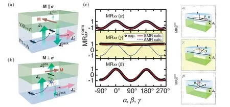
Fig.27.Illustration of the SMR effect.(a)When the magnetization aligns with the polarization of the spin current generated by SHE,its backflow reflection generates an ISHE current that contributes to the longitudinal current.(b)When the magnetization is perpendicular to the spin polarization,spin current is absorbed and no ISHE current affects the longitudinal current.(c)Magnetoresistance curves as a function of the angles α,γ,and β,illustrated in the right panel.The key contrast to conventional AMR is the trace in middle figure,where no dependence is observed,while conventional AMR would give the sinusoidal form illustrated in the dashed line.[87]
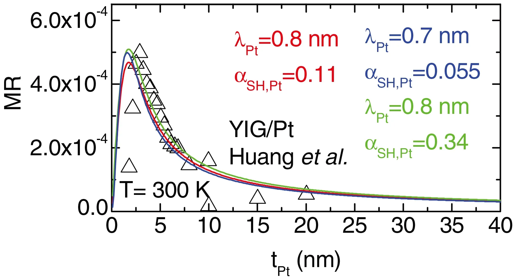
Fig.28.Dependence of the MR on tPt determined by different values for the spin-mixed conductance to fit the experimental curve,with differentand
Moreover,the SMR effect rectified the dynamic current flowing through the HM into a DC electrical signal by the dynamic magnetization in the FI material,which would be involved in SP or ST-FMR measurements. Because the applied dynamic magnetic field used for FMR excitation induced a dynamic electrical current in the HM layer,both SP signal and SMR rectification were interrelated from the very beginning.[86,91]However,it has been found that,for similar YIG/HM samples that were believed to present a pure SP signal,some experiments showed the existence of SMR rectification,[91]whereas others have not.[92]A consistent explanation for the discrepancy was lacking.
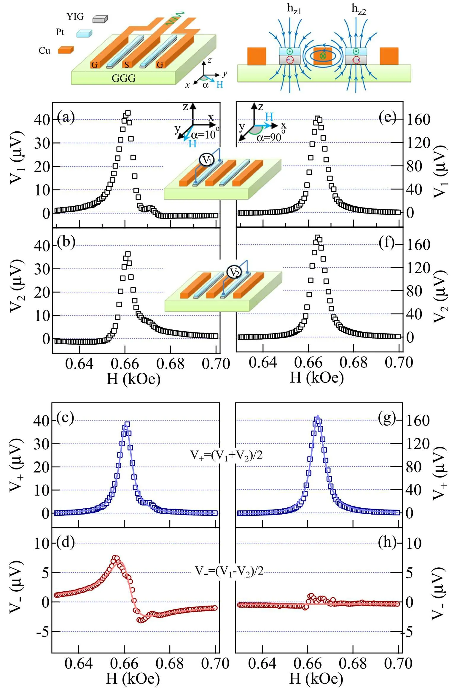
Fig.29.Diagram of our device wherein two identical Pt/YIG strips were placed symmetrically in the slots of a co-planar waveguide(CPW).A π phase difference is seen in the precession magnetization in the two strips due to the spatial distribution of the dynamic magnetic field generated by the CPW.(a)and(b)are voltage spectra of the left-hand side strip(V1)and the right-hand side strip(V2),and(c)and(d)are the sum(V+=V1+V2)and the difference(V−=V1 −V2)of those spectra,which correspond to SP and SMR rectification signals,respectively.The left(right)column is the data measured at a α=10◦(α=90◦),as indicated by the coordinate systems shown in the insets.[93]
The key difference between the nature of SP and SMR rectification could be understood from the viewpoint of spin dynamics. Although both SP and SMR rectification have a resonant feature,they depend on the dynamic magnetization in different ways.The SP signal is determined by the intensity of the time-independent spin current,which is proportional to the reduced time-averaged magnetization due to FMR.Therefore,the SP signal depends on the square of the amplitude of the dynamic magnetization,and shows only a symmetric Lorentz line shape.SMR rectification comes from the nonlinear coupling between(t)and(t)through the SHE,SOT,and ISHE.Therefore,the SMR rectification signal depends on the individual amplitudes of the dynamic current and dynamic magnetization and the relative phase in between.The phase-dependent nature of SMR rectification is the fundamental characteristic distinguishing it from SP.As a corollary,two identical FI/HM samples with a phase difference in magnetization dynamics will show inverse SMR signals along with the same SP,which has been tested by our experimental results as shown in Fig.29.
In the HM/FI systems and even in metallic bilayers,in addition to the above mentioned SMR,Grigoryan et al.[94]predicted a new type of MR effect wherein a Rashba-type SOI is present at the interface between HM and FI.This new spin–orbit MR(SOMR)works even with light metals such as Cu or Al,with negligible bulk SOI.Zhou Lifan(Nanjing University)et al.[95]first reported observation of SOMR in a Cu/YIG bilayer,where the Rashba spin–orbit interaction at the Cu/YIG interface was enhanced by an ultrathin Pt layer(<1 nm).According to Zhou Lifan et al.,the SOMR almost disappeared when Pt was placed inside or on the other side of the Cu layer,indicating that SMR from the ultrathin Pt layer could not be the origin of the observed MR and that the Pt decoration of the Cu/YIG interface was crucial for SOMR.An important feature was that the MR showed two maxima as the Pt layer thickness increased,in sharp contrast to that of SMR,as shown in Fig.30.
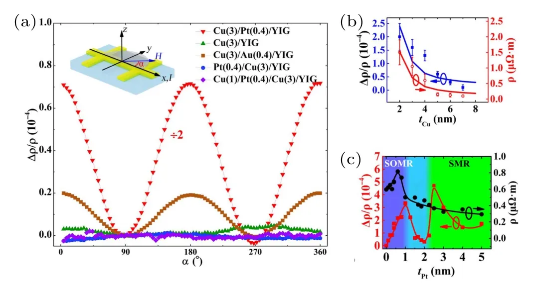
Fig.30. (a)Angular-dependent MR measurements in the xy plane for several control samples. (b)Cu thickness dependence of the MR ratio and ρ for Cu(tCu)[Pt(0.4)]/YIG.Solid lines are the Boltzmann simulation results. (c)Pt layer thickness dependence of the MR ratio and r for Cu(3)/Pt(tPt)/YIG.Solid lines are guides for viewing.[95]
3.4.Spin Seebeck effect
The Seebeck effect refers to the scenario wherein there is a temperature gradient in a conductor,and diffusion velocity of the electrons is different at different temperatures,leading to the nonequilibrium distribution of electrons in space,[96]and,in turn,leading to a potential difference within the conductor.The ratio of the resulting potential difference to the temperature gradient is called the Seebeck coefficient.The spin Seebeck effect(SSE)is the difference in spin potential in a ferromagnet caused by a temperature gradient.SSE can affect a pure spin current into an HM adjacent to an FM;the effect was first found in FMs,but was also observed in magnetic insulators shortly thereafter. In FM,the temperature gradient leads to different electron conduction behaviors with different spin orientations,leading to the generation of a spin current.In a ferromagnetic insulator,the temperature gradient causes the magnons to collectively oscillate,thereby generating a spin wave,which,in turn,produces a spin current.
Xiao Jiang(Fudan University)et al.gave a theoretical explanation of the spin transport of the SSE with magnons as carriers.[97]Adachi H et al.explained the SSE theoretically[23]as being caused by the difference between the magnon temperature in the FM and the electron temperature at the contact point of the HM with an equal phonon temperature. Observation of the SSE was designed through two kinds of experiments,the transverse SSE and the longitudinal SSE,as shown in Fig.31.For the transverse SSE,a quantitative formula to describe the relationship between the spin current and the temperature difference is as follows:[23]
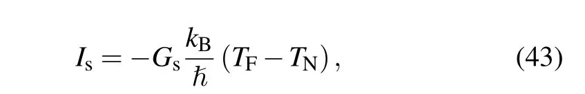
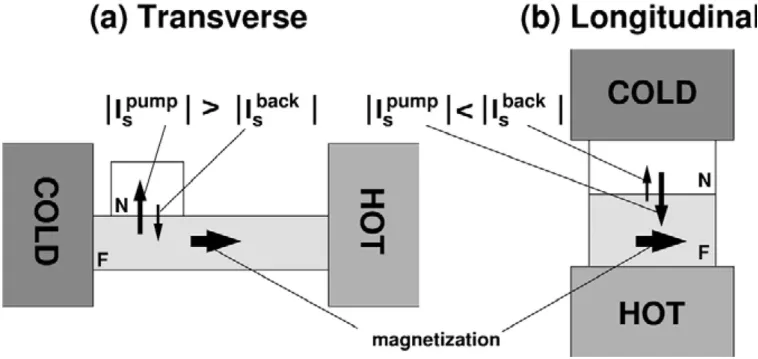
Fig.31.Schematic diagrams of the(a)transverse and(b)longitudinal spin Seebeck effects.[23]
Uchida et al.[98]used the SSE in the FI of LaY2Fe5O12to generate a spin current,as shown in the Fig.32.A magnetic field was applied to make the local magnetic moment align in the x direction,and a temperature gradient was applied in the x direction to generate a spin potential difference across the LaY2Fe5O12/Pt interface in the z direction.Consequently,a spin current was generated in Pt,which was detected by the ISHE.
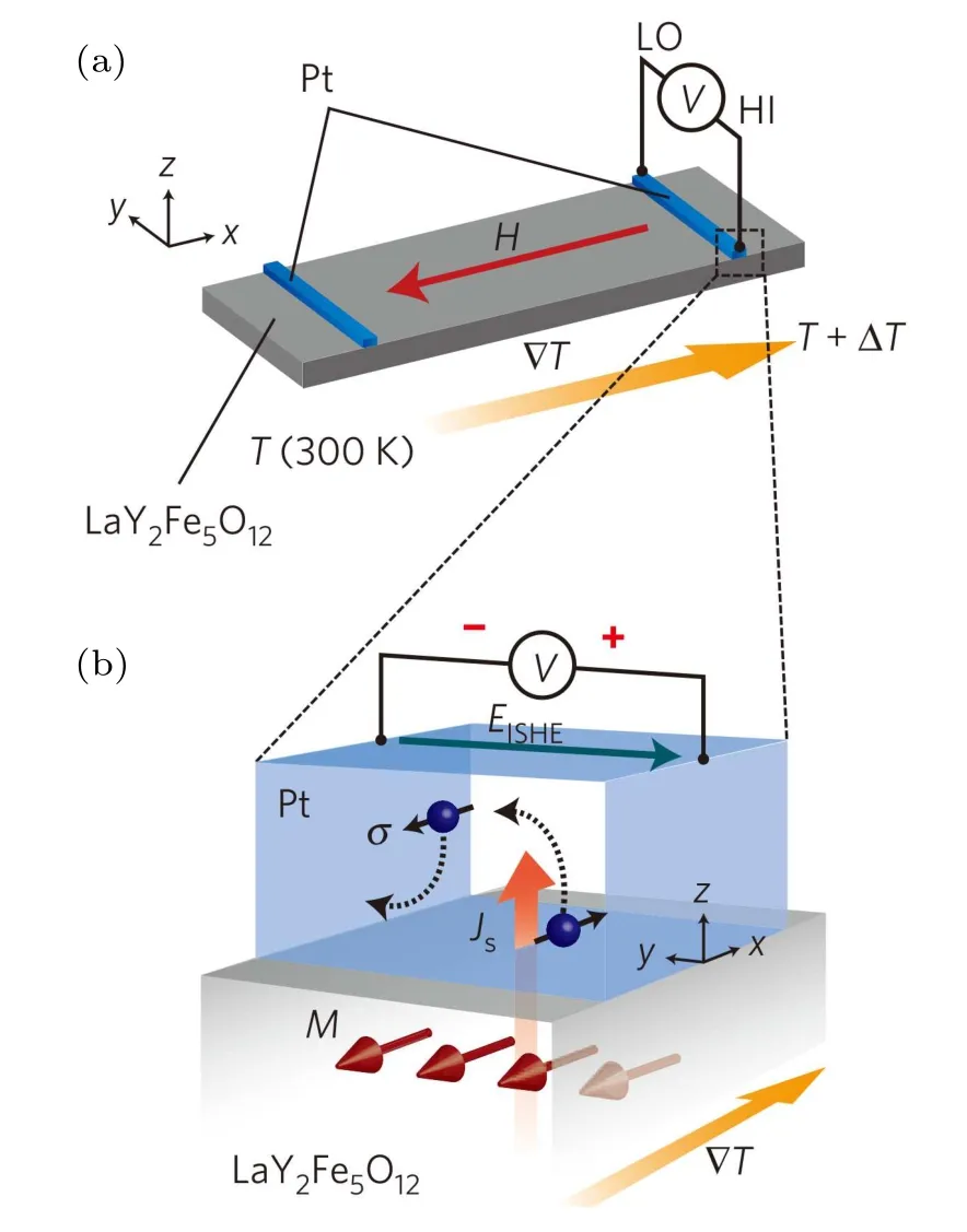
Fig.32. Schematic illustrations of the measurement set-up. (a)Sample consists of a LaY2Fe5O12 film with two Pt wires attached to the surface. (b)ISHE in the Pt wire and the spin current induced across the LaY2Fe5O12/Pt interface.[98]
As a further step toward device applications,a design of a Spin Seebeck Diode(SSD)was proposed in a spin-valve nanopillar geometry that allowed the thermal-induced spin current to flow only in one direction,which has the potential as a key unit in spin caloritronic devices. Fu Huahua(Huazhong University of Science and Technology)et al.proposed a SSD design using two-dimensional(2D)materials such as silicene and phosphorene nanoribbons as the source and drain.[99]As shown in Fig.33(a),the authors adopted a zigzag silicene nanoribbon(ZSiNR)heterojunction.The ZSiNR heterojunction in the SSD design had a double-hydrogenterminated ZSiNR(N-ZSiNR-H2)as the source and a single hydrogen-terminated ZSiNR(N-ZSiNR-H)as the drain.Calculations demonstrated that,by applying a temperature gradient between two contacts,spin-dependent currents with opposite spin directions were driven into the device and just flowed in opposite directions.Due to the appropriate control of the magnetization state,the energy band structure of the source and drain allowed almost perfect cancellation between thermally induced spin-up and spin-down currents that flowed in opposite directions with nearly equal magnitudes across the heterojunction.In addition,the authors found that changing the gate voltage could reduce the conductive current and optimize SSD performance.
Wu Hao(who graduated from Lanzhou University and currently at the Institute of Physics,the Chinese Academy of Sciences)et al.,[100]proposed a magnon valve made of two FI(YIG)layers separated by a nonmagnetic spacer layer(Au),as shown in Fig.34(a).When a thermal gradient was applied perpendicular to the layers,the ISHE signal from the Pt bar placed on top of the magnon valve depended on the relative orientation of the magnetization of two YIG layers,indicating the magnon current induced by the SSE at one FI affected the magnon current in the other FI separated by Au.In magnon valve structure,utilizing magnetic insulators rather than magnetic metals for spintronic devices showed superior advantages in terms of low energy consumption;the present results should open a door for fundamental research and device application beyond those based on conventional spin valve structures.
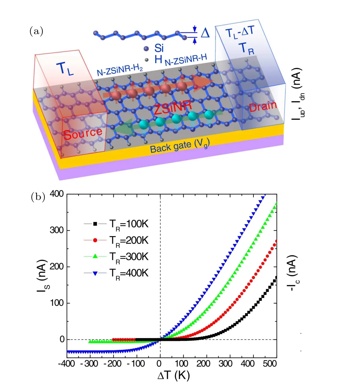
Fig.33.(a)Schematic of the ZSiNR-heterojunction-based spin caloritronics device,where the ZSiNR heterojunction is composed of N-ZSiNR-H2(source)and N-ZSiNR-H(drain)and placed on a substrate with a gate voltage.∆T represents the temperature difference between the source(TL)and the drain(TR),i.e.,TL −TR.(b)Change in spin current with ∆T.[99]
Miao Bingfeng (currently at Nanjing University) et al.[101]reported observation of the ISHE in a ferromagnetic permalloy(Py)on ferromagnetic insulator yttrium iron garnet(YIG)utilizing SSE.ISHE in the ferromagnetic metals was considered as the inverse effect of the AHE.Similar to ISHE in HM,one may expect ISHE in a FM to generate a transverse charge current and charge accumulation.To separate the signal contributions of the ISHE and the abnormal Nernst effect,the experiment used ion etching to change the YIG surface or to insert an insulating layer between the YIG/Py(Fig.35).In the experiment,it was found that Py has a relatively large θSH.With this method,one can explore the phenomenon of pure spin current in most FMs.
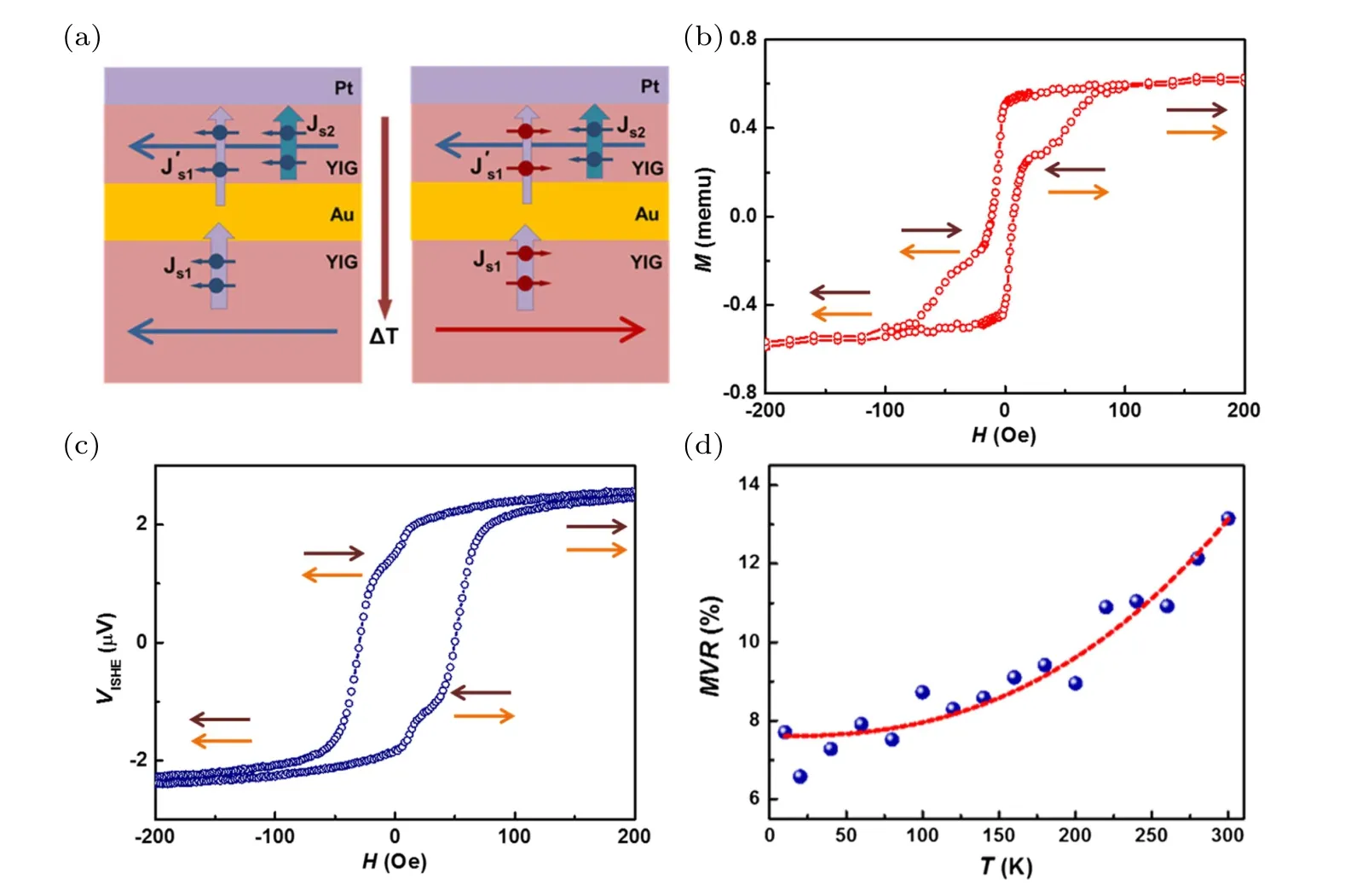
Fig.34.(a)Illustration of the magnon valve effect:When a temperature gradient is applied,the magnon current in the top YIG comes from two sources.One is generated by the presence of the local temperature gradient,the other is the magnon current injected from the bottom YIG layer.If the magnetization directions of the YIG layers are parallel(antiparallel),these two magnon currents are additive(subtractive).(b)Magnetization of the magnon valve as a function of in-plane applied magnetic field.(c)ISHE voltage in Pt as a function of the magnetic field.(d)Temperature dependence of MVR;dashed line shows the T 5/2 fitting curve.[100]
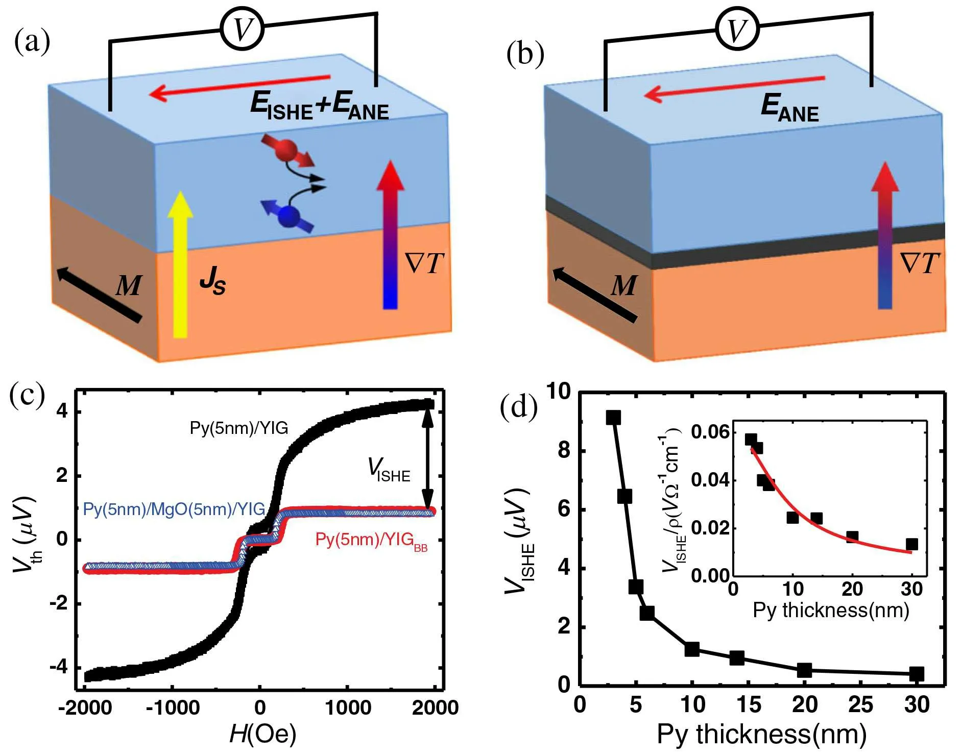
Fig.35.Schematic of(a)Py/YIG and(b)Py on altered YIG under a perpendicular temperature gradient.(c)Field dependence of the thermal voltage Vth for Py/YIG and Py/MgO/YIG.Voltage difference VISHE gives the contribution exclusive to the inverse SHE in Py.(d)Thickness dependence of the VISHE of Py/YIG.[101]
3.5.Light injection and light detection
The experimental discovery of the SHE was prompted by intrinsic SHE proposals that focused on semiconductors and suggested utilization of the optical activity of these materials for detecting the SHE.Similar to the original work by Dyakonov and Perel,Sinova et al.[29]proposed a circularly polarized electroluminescence,or spatially resolved magnetooptical Faraday and Kerr effects. These methods were,indeed,used in the first measurements of the phenomenon.Band structure in a semiconductor crystal can be divided into the conduction band and valence band.The band near the valence band top can be divided into the heavy hole band(HH)and light hole band(LH),according to the effective electron mass.When the SOC action in the lattice was considered,effective mass of the electron will change again,i.e.,an SOC band(SO)will split out from the valence band,as shown in Fig.36.
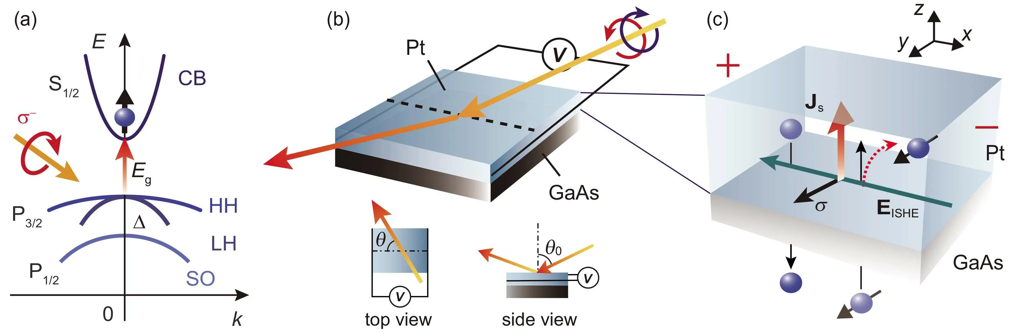
Fig.36.(a)Schematic illustration of the band structure of GaAs and spin-polarized electrons generated by the absorption of circularly polarized light.(b)Schematic illustration of the ISHE induced by photoexcited pure spin currents in the Pt/GaAs system.(c)Illumination angle θ dependence of measured for the Pt/GaAs hybrid structure.θ is the in-plane angle between the incident direction of the illumination and the direction across the electrodes attached to the edges of the Pt layer as shown in the inset.Filled circles are the experimental data.Solid curve shows a fitting result using a function proportional to sinθ.[102]
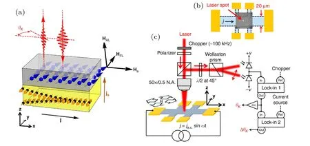
Fig.37.Detection of a Ta/CoFeB/MgO device’s spin orbital field by the optical method.(a)Schematic of the current-induced magnetization dynamics by SOFs.(b)Optical microscope image of the central region of the device,in which the laser(white spot)is tightly focused near the centre of the device.(c)Schematic of the experimental set-up depicting the IP current and magnetic field and the backscattering geometry of the probe laser beam.[50]
In 2010,Ando[102]reported an experiment in an HMsemiconductor hybrid structure in which they demonstrated the conversion of circularly polarized light absorbed in a semiconductor to an electrical signal in the attached HM ISHE sensor(Fig.36).The photoinduced ISHE was observed in a Pt/GaAs hybrid structure. In the GaAs layer,circularly polarized light generated spin-polarized carriers,inducing a pure spin current into the Pt layer through the interface.This pure spin current was converted into an electrical voltage due to the ISHE in the Pt. Systematic changes of the ISHE signal were observed upon changing the direction and ellipticity of the circularly polarized light,consistent with the expected phenomenology of the photoinduced ISHE.The observed phenomenon allowed the direct conversion of circularpolarization information into the electrical voltage and was used as a spin photodetector.Spin current density generated by the circularly polarized light method has the following relationship with the circularly polarized light intensity and the degree of polarization:
The use of circularly polarized light can be used to not only generate but also to detect a spin current.In addition to the detection of the spin current by the ISHE mentioned above,optical methods can also be used to detect the spin current.Light interacts with the magnetic moment of a metal or insulator through the magneto-optical Kerr effect.In 2004,Kato[30]first observed SHE in GaAs using the magneto-optical Kerr effect.A magneto-optical Kerr microscope(MOKE)has a high spatial and temporal resolution,which can be used to detect the spin state not only in metallic FMs but also in magnetic insulators.Montazeri et al.[50]directly detected the spin–orbit field in an HM/FMI system.They found that the precession behaviors of the in-plane and out-of-plane magnetic moments caused by the current could be obtained in nonlinear magnetooptical terms.As shown in Fig.37,the spin–orbit field in the magnetic structure of metal and insulator can be directly detected by the interaction between the light and magnetic moment.
4.Application of SOT
The technological relevance of SOT for the development of the next generation of MRAMs was pointed out in breakthrough reports by Miron et al.[53]and Liu et al.[16]They demonstrated that SOT switching of the recording magnet SOT-based MARM exhibited potential applications,having the advantage of the read and write currents not being coupled together,as shown in Fig.38;this avoids the endurance issue by not exposing the tunnel barrier to the writing current.In addition,SOT writing in a perpendicular anisotropy film stack can eliminate incubation time by engineering the spin polarization to be misaligned with the recording magnetization. Therefore,the in-plane writing current geometry can make the SOT more efficient and faster than STT.In the following section,we will review the recent progress in SOTinduced magnetization switching in FM/NM bilayers.
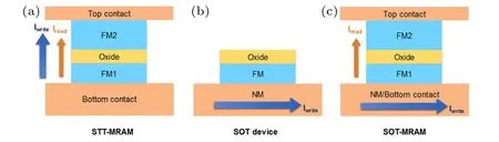
Fig.38.Schematic structures of(a)STT-MRAM,(b)SOT device,and(c)SOT-MRAM cell utilizing an SOT scheme for writing,and a TMR scheme for readout.[45]
4.1.SOT-induced magnetization switching in FM/NM bilayers
In typical FM/HM bilayers,as a charge current is injected into the HM layer,a transverse spin current can be generated in the HM layer or at the HM/FM interface by the bulk SOC or Rashba SOC,respectively.Accumulation of spin at the interface generates torques on the FM layer,which change the direction of the magnetic moment or move the domain wall inside the FM.The torque acting on the magnetic moment in the FM can be decomposed into two parts:the field-like torque and damping-like torque,as shown in Fig.39(a).Figure 39(b)shows a typical SOT-induced switching curve in a FM/HM bilayer with PMA,wherein Hall voltage is measured as a function of the amplitude of electrical current.

Fig.39.(a)Decomposition of the SOT acting on the magnetic moment,[103]wherein the vectors labelled as B and τ are the directions of effective field and torque.FL means“field-like”and DL means“damping-like.”(b)A typical loop representing current-induced magnetization switching in a FM/NM structure with perpendicular anisotropy.[45]
One of the issues in the application of SOT for MRAM is to reduce the critical current density required for the switching.Therefore,vast research works have been carried out to improve SOT efficiency and thus reduce the writing current by searching the materials with high SHA,employing different film stack or interface decoration.Moreover,deterministic magnetization switching in PMA structures using SOTs with in-plane spin polarization requires an external assist field to break the symmetry in the system.However,incorporation of this assist field is not practical in real applications due to reasons of scalability.Various approaches,such as structural and stack engineering,exchange biasing of a FM,and the use of ferroelectric substrates,have been employed to realize fieldfree switching.Next,we give a brief review of these research works.
4.1.1.Material and stack choices for SOT-induced magnetization switching
Generally,to improve the efficiency of SOT,the HM underlayer for the SOT studies must be heavy metals owing to their large SOC strength.The most widely used heavy metals for SOT devices include Pt,Ta,W,and Hf.Among these heavy metals,Pt is the most well-studied,having been found to have a large positive SHA,while W in β-phase shows the largest negative SHA.[104]In addition,AFM,two-dimensional material systems,or even topological insulators also show a large spin current generation efficiency.[105]
Besides the HM layer itself,the SOT exerted on the FM is also influenced by the bilayer interface scattering of the spin current.A few recent works have been devoted to study of the role of FM/HM interface transparency in the amount of spin currents diffusing into the FM.[82,106]In addition,it has also been found that the SOT strength can be enhanced by modulating spin absorption using a proper capping layer.Qiu Xuepeng(currently at Tongji University)et al.studied the Pt/FM/Ru structure[107]and found that the capping layer Ru had a great promoting effect on the absorption of the spin current in the FM layer;therefore,the SOT acting on the magnetic moment in the FM layer was also enhanced significantly by the Ru capping layer.
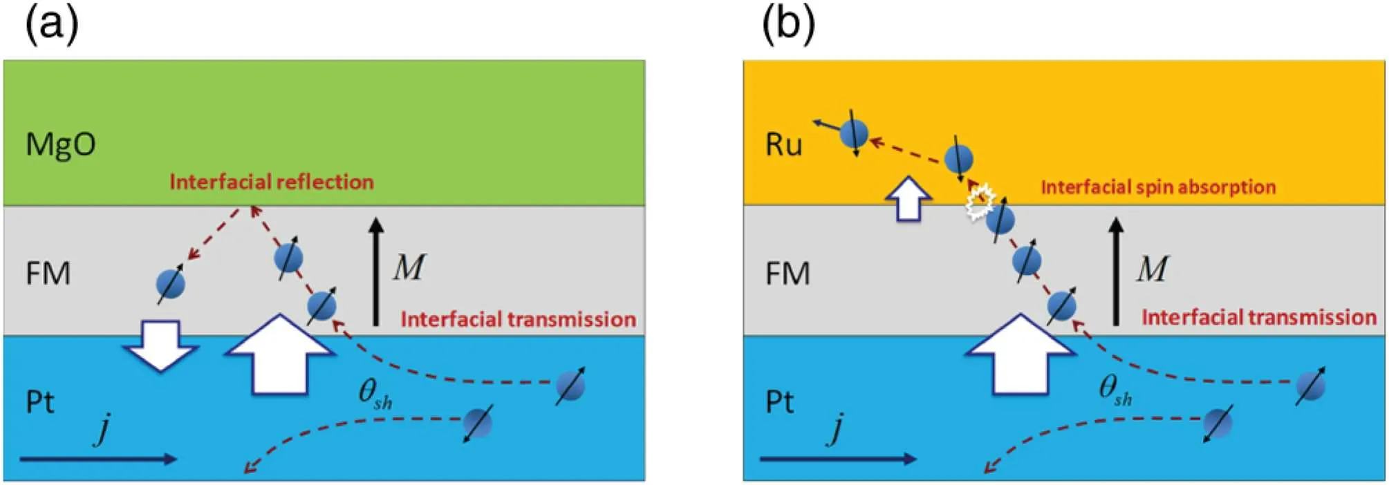
Fig.40.(a)In a Pt/FM/MgO structure,polarized spins from the Pt layer are partially reflected at the FM/MgO interfaces and compensate the torque at the Pt/FM interface.(b)In a Pt/FM/Ru structure,with strong spin relaxation near the FM/Ru interface,the absorption of spin currents from the Pt layer into FM is greatly enhanced.White arrows denote the spin currents.[107]
In addition,an effective way to obtain large effective SHA is based on HM/FM/HM systems,in which two HMs show opposite signs of SHA.Yun Jijun(Lanzhou University)et al.[108]studied the SOT-induced magnetization switching in Pt/Co/Ta stacks with perpendicular magnetic anisotropy,as shown in Fig.41(a). They found a large effective SHA around 0.356 that was ascribed to the opposite signs of SHE for Pt and Ta.However,the magnitude of SHA decreased when the Ta layer was thicker than 4 nm,which could be explained by the different crystallinity of Ta.Figure 41(b)shows the XRD patterns,in which the(202)peak for β-Ta phase located at ∼38.0◦,and the(220)peak for Pt located at ∼67.5◦.Although both Pt(5)/Co(0.5)/Ta(4)and Pt(5)/Co(0.5)/Ta(8)showed the existence of β-Ta phase,which was a guarantee for a large SHE effect,the full widths at half maximum(FWHM)of β-Ta(202)peaks for these two sample were apparently different.
Although the above investigations mainly focused on choosing HMs with large SHA or those structures with large effective SHA to improve the SOT’s efficiency,the critical switching current,Jc,was found not only to be related to the strength of the effective SOT,but also to the perpendicular magnetic anisotropy field.Therefore,interface decoration was employed for making an optimized balance between them and decreasing the critical current.Li Dong(Lanzhou University)et al.[109]found that,when a C interlayer was inserted between Co and Ta(Pt/Co/C/Ta),both the anisotropy field and the effective SHE torque per unit current density were reduced by nearly half through C decoration because of the change in interfacial magnetic anisotropy and the formation of defects during C sputtering.This result indicated that the interface modification by the C inserting layer could be used to reduce the current density of SOT-induced switching.
It has been previously proved that ion irradiation can be used to effectively tailor the magnetic properties of a magnetic material,which can be applied to decrease the critical current for SOT switching.In a recently published work from Yun Jijun(Lanzhou University)et al.,[110]the authors found that the irradiation process resulted in notable changes in coercivity,the anisotropy field,and the DMI effective field in Pt/Co/Ta structures as the data shows in Figs.42(a)and 42(b),although Jccould be significantly reduced.Such improvement resulted from the fact that the SOT was almost invariant after irradiation due to the nearly unchanged crystallinity of Pt and Ta layers,although the perpendicular magnetic anisotropy decreased because of irradiation-produced,enlarged roughness at the Pt/Co interface.
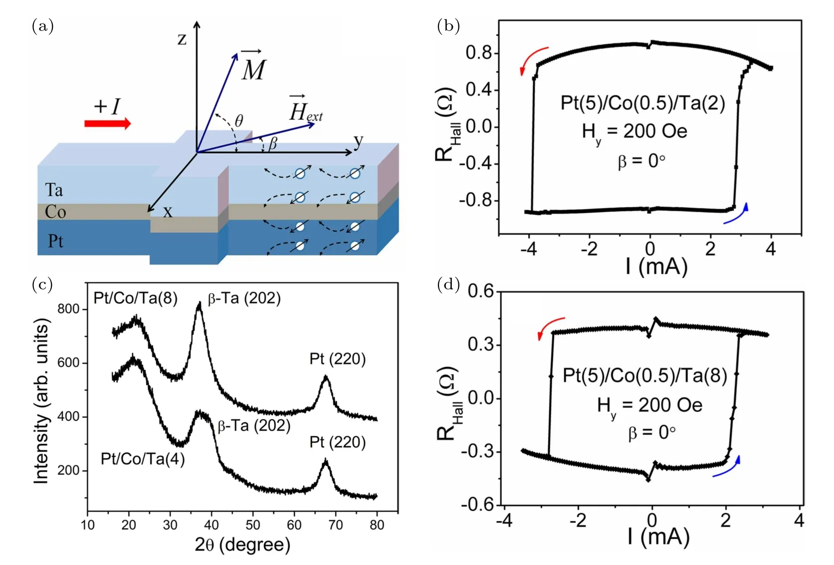
Fig.41.(a)Schematic illustration of Pt/Co/Ta stacks in the Hall bar structure for anomalous Hall resistance measurement under an external field,Hext,and a charge current I.(b)XRD patterns for Pt(5)/Co(0.5)/Ta(4)and Pt(5)/Co(0.5)/Ta(8)film stacks.Current induced switching for(c)Pt(5)/Co(0.5)/Ta(2)and(d)Pt(5)/Co(0.5)/Ta(8).[108]
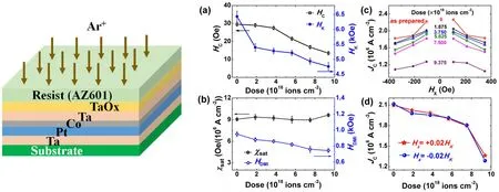
Fig.42.Schematic and experimental results of Ar+irradiation taken at normal incidence on samples.(a)Ion dose dependence of the coercivity and perpendicular anisotropy field.(b)SOT efficiency and DMI effective field as a function of ion dose.(c)Critical switching current density as a function of in-plane bias field at different doses.(d)Dose dependence of Jc.[110]
4.1.2.SOT-induced field-free magnetization switching
Another issue in the application of SOT-MRAM is that SOT-induced deterministic magnetization switching requires an external assist field to break the symmetry in PMA systems. In a pioneering study,the researchers applied an inplane magnetic field of several hundred to a thousand Oersteds to obtain deterministic magnetization switching.However,from a practical point of view,it was difficult to integrate such a large bias field into the storage cells by engineering a film stack.Therefore,researchers have been looking for a way to achieve field-free switching. Yu Guoqiang(currently at Institute of Physics,Chinese Academy of Sciences)et al.[111]achieved field-free deterministic magnetization switching in a Ta/Co20Fe60B20/TaOxstructure by introducing a lateral structural asymmetry. In their work,a wedge-shaped TaOxlayer produced a field-like SOT due to the Rashba effect,with an effective magnetic field along the z-axis that facilitated currentinduced deterministic switching.Thus,the asymmetrical geometric shape provided an effective means of achieving deterministic switching. Moreover,factors such as exchange bias[111]and interlayer coupling[112]could be used to generate an effective in-plane field that broke the symmetry of the system to realize a SOT-driven,field-free switching.
So far,in the methods discussed to achieve external fieldfree switching,it has not been possible to alter the direction of the effective magnetic field(wedged structured),or there was a requirement of an external magnetic field cooling technique to change the direction of the effective magnetic field(AFM or exchange coupling).Cai Kaiming(Institute of Semiconductors,Chinese Academy of Sciences)et al.[113]reported that a field-free SOT switching could be reached with a ferroelectric/ferromagnetic hybrid structure. They demonstrated that the direction of the effective magnetic field for SOT switching could be programmed using electric means.As shown in Fig.43(a),Pt/Co/Ni/Co/Pt layers were deposited on a PMN-PT substrate and patterned for Hall bar measurements.A voltage VPMN−PTwas applied to set the initial polarization of the ferroelectric substrate. Before the substrate was polarized,the magnetization deterministically switched to a fixed z-direction,regardless of whether the current was applied along the x or −x direction.After applying a voltage of+500 V to polarize the ferroelectric substrate along the x-axis,a clockwise hysteretic loop of magnetization versus current density curve was reproducibly observed(Fig.43(b)). The loop then became anticlockwise after applying a voltage of−500 V(Fig.43(c)).Gradient of the spin densities caused by the polarization of PMN-PT produced an extra torque,which enabled the voltage-controlled deterministic switching.
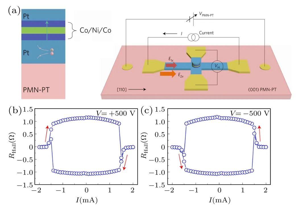
Fig.43.(a)Structure of the device,together with a typical cross-section of the deposited stack,with the green arrow showing the magnetic easy axis of the Co/Ni/Co(b),and(c)the current-induced magnetization switching after the polarization with+500 V and −500 V on PMN-PT substrate.[113]
Kong Wenjie(Institute of Physics,Chinese Academy of Sciences)et al.[114]studied the magnetic moment reversal driven by SOT in a coupled T-type structure.The T-type structure had two magnetic layers(CoFeB/Ta/CoFeB),as shown in Fig.44,with the upper FM having an in-plane anisotropy(IMA)and the lower FM having a PMA.The easy axis of the PMA layer was inclined slightly to realize the symmetry destruction of the system.This mode could enable a current applied along the in-plane,hard axis of the in-plane layer to switch both perpendicular and in-plane layers at the same critical current without applying magnetic field,i.e.,the type-T switch mode proposed by the authors.
Fig.44.Breaking symmetry with a T-type structure to achieve a field-free switching. (a)SOT-switching type-T mode. Green,red,and blue arrows denote current,magnetization of the PMA layer,and magnetization of the IMA layer,respectively.(b)Simulated spin polarization dependence of M1z and M2y in type-T mode,in which the current is vertical to EA of the IMA layer.[114]
4.1.3.Microscopic mechanism of SOT-induced magnetization switching
In the works discussed above,a macrospin model was normally used to explain the role of the in-plane magnetic field for the SOT-induced magnetization switching,which is required to break the symmetry of the current-induced,damping-like field with respect to the“up”or“down”magnetization states.However,for devices of micron dimensions,a macrospin description is clearly inadequate to provide an accurate quantitative understanding of the reversal process because of the presence of the spatially nonuniform reversal process.The current-induced DW depinning model proposed by Lee et al.[115]gave a better understanding of the magnetization reversal process and the role of the in-plane field in SOT-induced magnetization switching. They suggested that the function of the field was to orient the magnetic moments within the DW to align a significant component parallel to the current flow,thereby allowing the torque from the SHE to produce a perpendicular equivalent field that could expand a reversed domain in all lateral directions.
Cao Jiangwei(Lanzhou University)et al.[116]conducted a systematic analysis of SOT-induced magnetization switching in Ta/CoFeB/MgO structures under various in-plane magnetic fields.They observed asymmetric current-induced DW propagation process under various in-plane magnetic fields using MOKE microscopy. In addition,by analyzing the in-plane,field-dependent spin torque efficiency measurements,they obtained an effective field value for the DMI field of ∼300 Oe in a Ta/CoFeB/MgO structure,which played a key role in stabilizing Néel walls in the film stack.Finally,through micromagnetic simulations of the DW structure with the inclusion of DMI effects,they identified the origin of the current-induced,asymmetric DW propagation and the role of the in-plane field in SOT-induced magnetization reversal.
Fig.45.Current-induced DW propagation process in a Hall bar device with a medium in-plane field applied(Hx ≈0.5 HDMI)(a)–(h),and schematics of the magnetic moment orientation near DW and the corresponding SHE effective and Oersted fields induced by the current(i)–(k).[116]
4.2.SOT-driven domain wall and skyrmion motion
Current-induced domain wall and skyrmion motion is another prospective application of the SOT effect in the information-storage field. In 2008,Parkin[117]proposed the concept of racetrack memory.In this type of memory,magnetic domains were used as storage units,which were driven by the STT effect.Similar to the process of DW motion driven by STT,the SOT effect can also be used to drive DW motion,which has been found to be significantly faster compared to previous observations in NiFe or Co/Ni films driven by STT.Key issues to be solved include how to reduce the critical current density of the domain wall driven by current,which is,again,related to the SOT efficiency of the HM layer,pinning field,and anisotropic field of the FM layer,etc.
Li Dong(Lanzhou University)et al.[118]performed the research on SOT-driven DW movement in Pt/Co/Ta systems with PMA.They found that current-induced DW velocity was around 1000×larger than that in field-induced DW motion with a current-generated effective field keeping the same magnitude as the applied magnetic field,and that the current-generated Joule heating had an influence on DW motion.Moreover,current-induced DW tilting phenomenon was observed,demonstrating that the current-generated Oersted field may also play an essential role in DW tilting as shown in Fig.46. These findings could provide some designing prospects to drive DW motion in SOT-based racetrack memories.
Fig.46.(a)Kerr images give the definition of DW tilt angle(ψ)and changes of ψ at different current densities from“up”to“down”state and“down”to“up”state,taking the Pt/Co/Ta sample as an example. DW tilt angle versus current density for Pt/Co/Ta(b)and Pt/Co/C/Ta(c).The insets in(b)and(c)represent the snapshots of the domain shape at different current densities.[118]
The gradient of the magnetic anisotropy field can also be used as an effective magnetic field to manipulate DW movement driven by SOT.Zhang Yue(Huazhong University of Science and Technology)et al.[119]found that when a magnetic anisotropy gradient existed in a material,the enhanced anisotropy along the track acted as a barrier to inhibit the motion of the DW;however,reducing the magnetic anisotropy constants pushed the DW to move at a substantially higher speed. They also found that the DW type changed with increasing current density due to the action of SOT.As shown in Fig.47,when the current density increased from 0 to 1×10¹¹A/m2,the DW type was Néel type,and velocity of the DW rapidly increased from 0 to 20 m/s.With a further increase in the current density,the DW tended to become Bloch-type.At this time,with an increasing anisotropy constant,velocity of the DW was different for the negative and positive current density.This anisotropy control of the speed was of great significance in the design of new magnetic information devices with high reading speeds.
Magnetic skyrmions with non-zero spin winding number are compact magnetic textures with a non-trivial topology,so that they cannot be removed by a continuous perturbation. In 2013,Fert proposed replacing magnetic domains with skyrmions as the storage unit in racetrack memory.With the advantages of small size and stability,application of skyrmions in racetrack memory greatly increased storage density and stability.In addition,theoretical research shows that skyrmions can also be applied to spin nano-oscillators and transistors.[120,121]
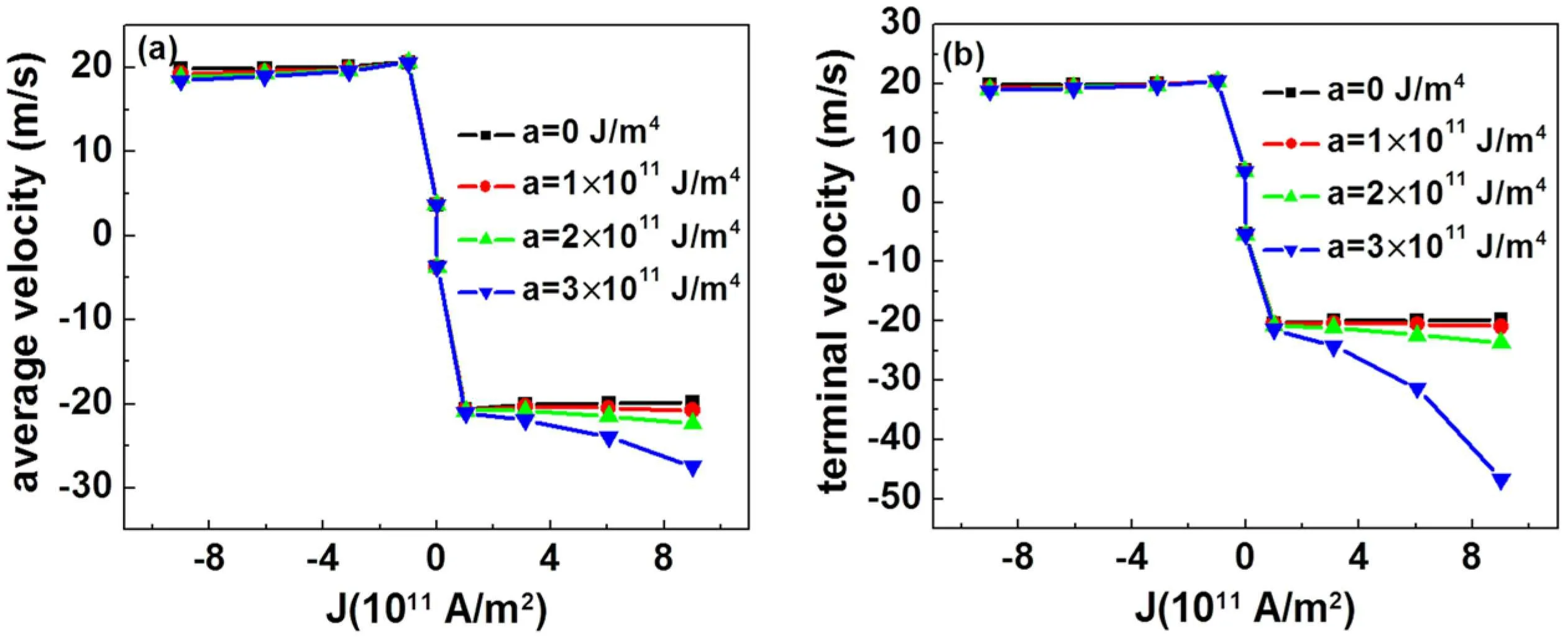
Fig.47.Influence of magnetic anisotropy gradient on the domain wall motion driven by SOT.Current density dependencies of the(a)average DV velocity,and(b)terminal velocity.[119]
In magnetic materials,the appearance of skyrmions originate from the competition between the Heisenberg exchange interaction and the DM interaction in the system.The Heisenberg exchange interaction can be expressed as follows:
The DM interaction is as follows:
where J is the exchange constant,andare neighboring atomic spins,and the DMI vector Dijis dictated by the crystal symmetry.
There are generally two sources of DM interactions:bulk and interface DMI effects. Bulk DMI can generate Blochtype skyrmions,which normally exist only at low temperatures and with an external magnetic field applied,whereas interface DMI can induce Néel-type skyrmions,which can be stable over a wide range.As a charge current is injected into the heavy metal layer,a spin current is generated in the vertical direction due to the strong SOC in the heavy metal layer.The upward spin current can penetrate through the HM/FM interface and exert SOT on the skyrmions in the FM,which finally drives the motion of skyrmions.[120]
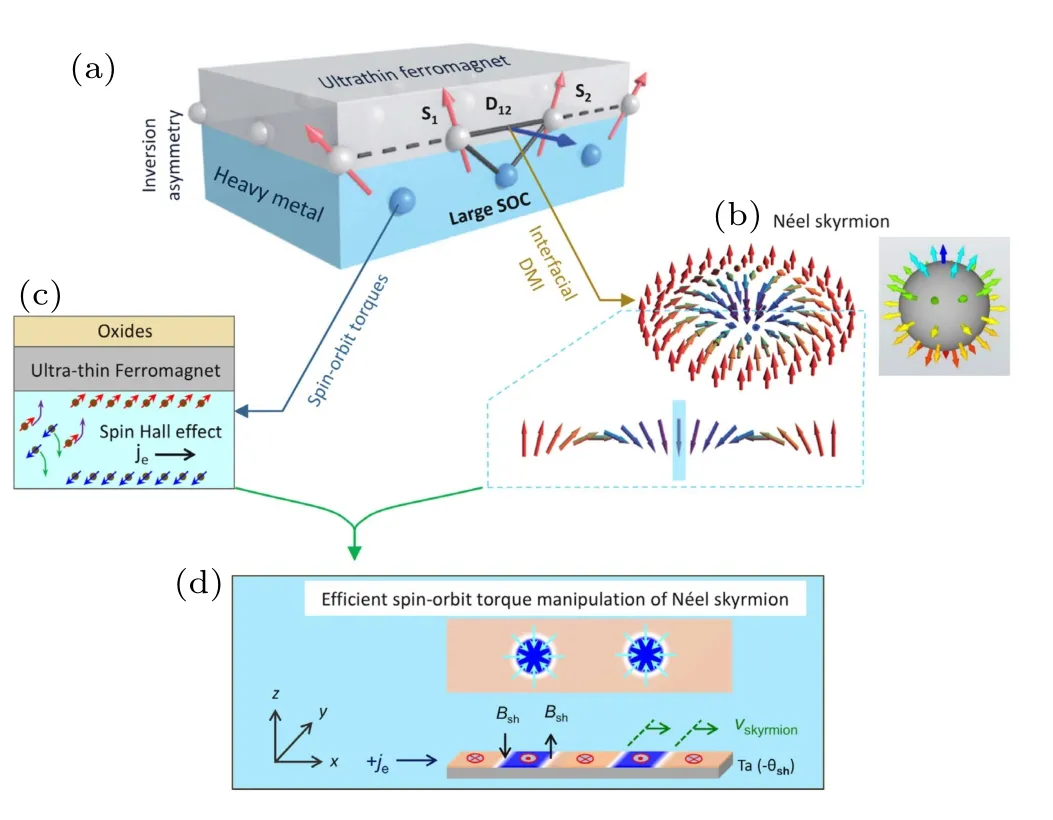
Fig.48.SOT control of skyrmions.[122]
Generation and manipulation of the single skyrmion at room temperature is a basic requirement for the application of skyrmions as the information carriers.Jiang Wanjun(who graduated from Lanzhou University and currently at Tsinghua University)et al.[121]successfully demonstrated the generation of skyrmions at room temperature using an inhomogeneous in-plane current in a Ta/CoFeB/MgO system lacking inversion symmetry.In a specially-designed device,as shown in Fig.49,the charge current was nonuniformly distributed.This nonuniform current caused the direction of the SOT acting on the striped magnetic domain to be different,eventually leading to the formation of skyrmion bubbles.
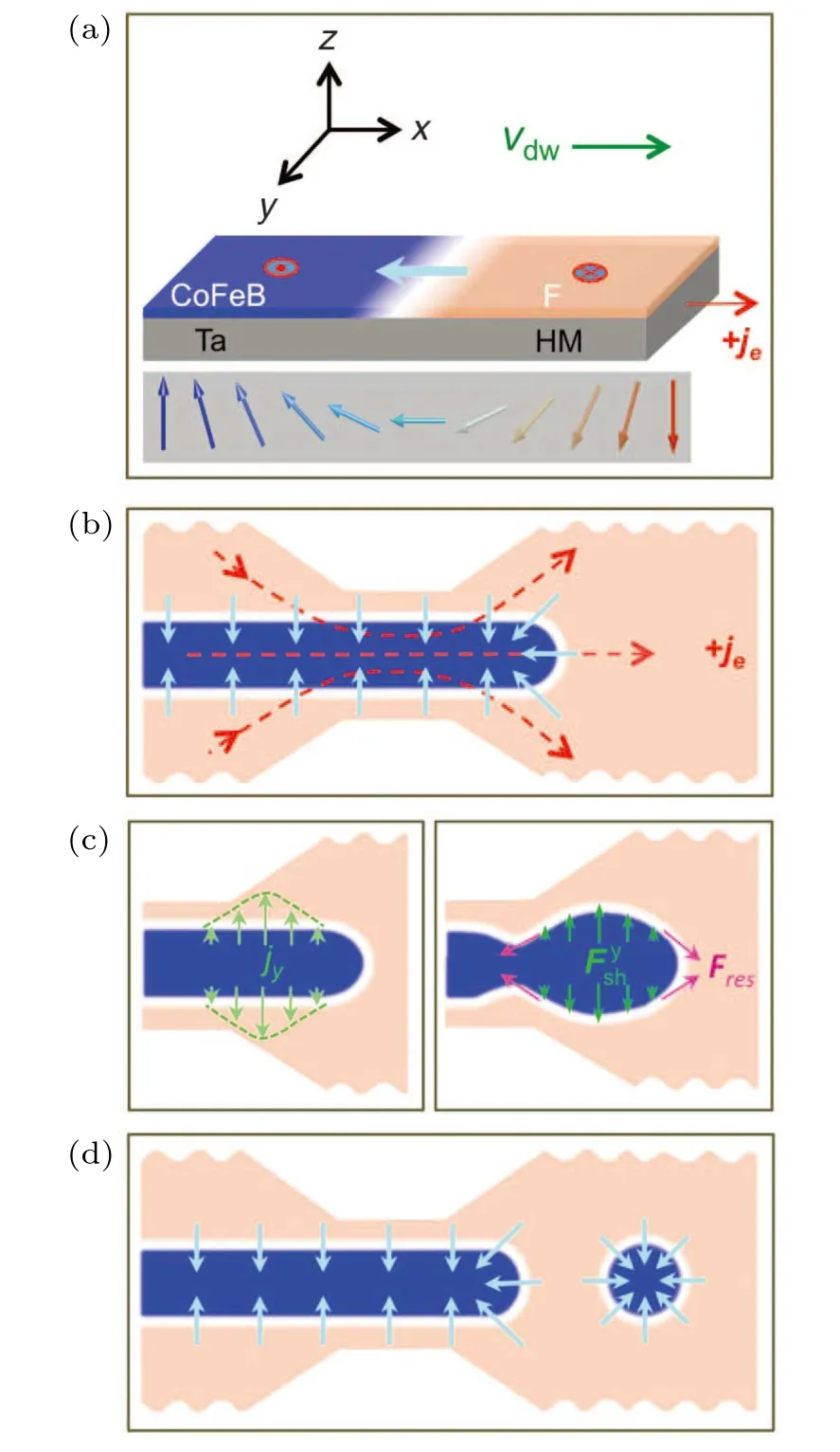
Fig.49. Generation of skyrmion bubble using current. (a)In a FM/HM bilayer,a homogeneous electron current je drives the chiral DW motion through the SOT.(b)Introducing a geometrical constriction into the device gives rise to an inhomogeneous current distribution.(c)and(d)The stripe domains break into circular bubble domains,resulting in the formation of synthetic Néel skyrmions.[121]
The charge current can be used not only to generate skyrmions but also to drive their motion along the track,as shown Fig.50.Since the required pulse width that drives the skyrmion is shorter than that for skyrmion generation,the generation and motion of skyrmions can be achieved by simply controlling the pulse width of the current.[123]This work is considered to be an important step toward the application of skyrmions in racetrack memory.
The applications of magnetic skyrmions in racetrack memories are mainly based on the motion of skyrmions in confined geometries. However,after application of the current,the skyrmion propagation direction exhibits an angle with the direction of current because of the skyrmion Hall effect.[124]Also,there exists a threshold current density above which the skyrmion is expelled and annihilated at the edge of the racetrack.The skyrmion Hall effect constrains the upper limit of the skyrmion propagation speed in the racetrack.Thus,manipulating skyrmion position and velocity with effective control methods is a challenge.
Fig.50.Generation and manipulation of multiple skyrmions using a pulsed current.[123]
In 2017,Song Chengkun(Lanzhou University)et al.[125]proposed a skyrmion-based multi-channel racetrack memory where the skyrmion moves in the selected channel by applying voltage-controlled magnetic anisotropy gates. It was demonstrated numerically that a current-dependent skyrmion Hall effect could be restrained by the additional potential of the voltage-controlled region,and the skyrmion velocity and moving channel in the racetrack could be operated by tuning the voltage-controlled magnetic anisotropy,gate position,and current density,which offered a potential application of racetrack memory based on skyrmions.
Twisted skyrmions,whose helicity angles are different from those of Bloch and Néel skyrmions,have recently been demonstrated in experiments.[126,127]Jin Chendong(Lanzhou University)et al.investigated the current-induced motion of twisted skyrmions by using micromagnetic simulations.[128]They found that the skyrmion Hall angle of twisted skyrmions driven by SOT varied continuously with helicity,which meant that the skyrmion Hall angle depends significantly on the helicity in addition to the dissipative force tensor and Gilbert damping,making it possible to achieve the SHE-induced motion of twisted skyrmions with a zero skyrmion Hall angle.
Fig.51.(a)Skyrmion-moving states in the multichannel racetrack when applying the electric field on Gate-1.Three moving states,in(b)channel 1,(c)channel 2,and(d)channel 3,could be well-controlled by the amplitude of electrical voltage.[125]
Fig.52. Four types of skyrmions:(a)–(d)Magnetization distributions of the twisted skyrmion,Bloch skyrmion,Néel skyrmion,and antiskyrmion,respectively.Red,white,and blue colors represent areas where the z-component of magnetization was positive,zero,and negative,respectively.Black arrows denote distribution of the in-plane magnetization.(e)–(h)Spatial profiles of the local magnetization corresponding to the yellow dotted line marked in(a).(i)–(l)Configurations of twisted DMI,bulk DMI,interfacial DMI,and anisotropic DMI,respectively.Orange arrows denote directions of the DMI vector.[128]
4.3.Application of SOT in AFM
AFMs have zero net magnetization are insensitive to external magnetic fields,making the magnetic order in AFMs difficult to manipulate and detect. On the other hand,these properties also make the AFM a potential candidate for highdensity,high-stability devices. More importantly,the high precession frequency of AFMs offers the potential for higher speeds of spintronics devices than those of their FM counterparts.Although antiferromagnets are hard to control by external magnetic fields because of their alternating magnetic moment directions on individual atoms and the resulting zero net magnetization,SOT has proven to be an effective way of modulating magnetic order in a certain class of antiferromagnets.
In 2016,Wadley et al.[129]reported a current-induced switching of the AFM order in CuMnAs,setting a milestone for the manipulation of the staggered order parameter.In such material,where the breaking of inversion symmetry occurs at the sublattice level,opposite spin polarizations are induced in the two(inversion-partner)sub-spin lattices,via the Edelstein effect.The ensuing field-like torque can reorient the Néel order whenever this field overcomes the threshold given by the in-plane anisotropy(several tens of Oersteds),as dictated by the effective energetics of the order parameter. At present,only a few antiferromagnets such as CuMnAs and Mn2Au can meet this demand.[130]
In 2018,Zhou Xiaofeng(Tsinghua University)et al.[131]reported orientation-dependent Néel-order SOT switching in single-layer Mn2Au films with different switching features for different orientations.Using short current pulse at room temperature,the authors demonstrated a reversible switching that was attained in Mn2Au(103)films due to negligible magnetocrystalline anisotropy energy,as shown in Fig.53,while for Mn2Au(101)and(204)films,the switching was invertible with the current applied along the in-plane easy axis and its vertical axis.However,it became seriously attenuated during initial switching circles when the current was applied along the hard axis because of the existence of magnetocrystalline anisotropy energy.
Since magnetic anisotropy energy is quite important in the current switching of single-layer Mn2Au films,Chen Xianzhe(Tsinghua University)et al.[132]employed a ferroelastic strain from a ferroelectric material to switch the uniaxial magnetic anisotropy(UMA)of an adjacent antiferromagnet.Due to the electric field controlled UMA,the authors observed an asymmetric Néel SOT in the Mn2Au,which was used to demonstrate an AFM ratchet,as shown in Fig.54.Asymmetry of the Néel SOT and the corresponding AFM ratchet could be reversed by the electric field,which subsequently controlled the NSOT switching.
Recently,AFM skyrmions have been predicted in AFM materials due to the presence of bulk DMI. The AFM skyrmion is comprised of two coupled topological spin configurations with opposite topological numbers. When AFM skyrmion motion is driven by SOT,the skyrmion Hall effect in opposite directions cancel each other out due to their opposite topological numbers Therefore,the AFM skyrmion can move along the injected current without deflection. Jin Chendong(Lanzhou University)et al.compared the motion of AFM skyrmions and FM skyrmions driven by used micromagnetic simulations,as shown in Fig.55.[133]The authors found that the AFM skyrmion had three evident advantages:(i)minimum driving current density of the AFM skyrmion was about two orders smaller than that of the ferromagnetic skyrmion;(ii)velocity of the AFM skyrmion was about 57×larger than that of the ferromagnetic skyrmion driven by the same value of current density;and(iii)the AFM skyrmion could be driven by the SHE without the influence of magnus force.In addition,the AFM skyrmion could move around the pinning sites due to its property of topological protection. Those results presented an understanding of AFM skyrmion motion driven by the SHE and may also contribute to the development of AFM skyrmion-based racetrack memories.
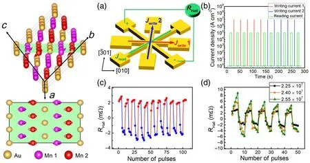
Fig.53. Schematic of two(inversion-partner)sub-spin lattices in Mn2Au(103)films. (a)Schematic of the star device and switching measurement geometry.Writing current pulses are applied along the red(Jwrite1)and blue arrows(Jwrite2)alternatively,corresponding to two orthogonal directions for Mn2Au(103)films.(b)Sketch of alternative writing current pulses along two orthogonal directions.(c)Hall resistance change as a function of the number of writing current pulses.(d)Comparison of the variation in RHall with different magnitudes of writing current pulses.[131]
Fig.54. (a)and(b)Schematic of ferroelastic strain switching of UMA driven by electric fields in an antiferromagnet/PMN-PT(011)structure.(c)Measurement configurations for the Néel SOT.(d)Schematics of the ratchet-like behavior based on the asymmetric Néel SOT switching when the magnetic easy axes are aligned along the(top)or[011](bottom)direction.(e)Transverse resistance variation of the Mn2Au device as a function of the number of current pulses after applying different E.Original state as well as E=+4,−2,and+4 kV·cm−1 scenarios are shown in panels(i),(ii),(iii),and(iv),respectively,in order of measurement sequence.The colors of symbols for the data correspond to the writing current channels.[132]
Fig.55.Comparison of the motion of AFM and FM skyrmions driven by the SHE.(a)Velocity of the Bloch AFM skyrmion and Bloch FM skyrmion as a function of current density.Top-views of(b)Bloch FM skyrmion,and(c)Bloch AFM skyrmion motions derived by SOT.[133]
5.Prospects
From the 1990s to the present,the development of spintronics has experienced three explosions.In the 1990s,GMR and TMR led the trends in the new generation of magnetic storage.At the beginning of the 21st century,semiconductor spintronics produced by the combination of spin and semiconductors set off an upsurge in research and became the research frontier of that time.Recently,the research hotspots of spintronics have focused on concepts such as the STT effect,SHE,the SOT effect,spin dynamics related to thermal effects.[32]Although spintronics have evolved rapidly,we are still in the exploratory stage of manipulating spin.
The great application prospects of spin-current have drawn the attention of several researchers.The study of spincurrent can promote the early realization of magnetic storage using local current to manipulate magnetic nanodevices.The magnetic moment controlled by electric current can greatly improve magnetic storage density,which will have a huge impact on the information industry,quantum computing,and even life science,possibly directly determining the progress of a country and even of the whole of mankind.Successful implementation of the commercial application of SOT-MRAM is our ultimate goal,and we believe that the future of spintronics will bring more surprises.
猜你喜欢
杂志排行

Chinese Physics B的其它文章
- Theoretical analyses of stock correlations affected by subprime crisis and total assets:Network properties and corresponding physical mechanisms∗
- Influence of matrigel on the shape and dynamics of cancer cells
- Benefit community promotes evolution of cooperation in prisoners’dilemma game∗
- Theory and method of dual-energy x-ray grating phase-contrast imaging∗
- Quantitative heterogeneity and subgroup classification based on motility of breast cancer cells∗
- Designing of spin filter devices based on zigzag zinc oxide nanoribbon modified by edge defect∗