二维铁电材料ABP2X6内在极高的负泊松比
2019-10-14张春梅聂亦涵杜爱军
张春梅,聂亦涵,杜爱军
昆士兰科技大学科学与工程学院,化学物理与机械工程系,澳大利亚,昆士兰州,布里斯班 4001
1 Introduction
Negative Poisson’s ratio (NPR) materials, known as auxetic materials, behave expansion instead of contraction under tension, which have attracted intensive research interests,because these materials exhibit novel properties such as enhanced toughness and enhanced sound or vibration absorption1. NPR is mainly observed in engineered threedimensional bulk structures2, but only several twodimensional (2D) auxetic materials are proposed, which are monolayer Be5C23, black phosphrous4, BP55, SnSe6, pentagraphene7, silicon dioxide8, borophene9,10, and TiN11. These materials possess re-entrant or hinged geometric structures,which is the main reason of auxetic behaviour. Among them,the largest NPR value reported is -0.17 in monolayer SnSe6,which is quite low for realistic application. Moreover, the technological evolution requires that the electronics to be of a smaller size12,13. Thus, the exploration of auxetic nanomaterial with high NPR is highly demanded. Considering that NPR is mainly structure-oriented, more attentions should be paid into nanomaterials with particular geometry structure for exploring 2D auxetic material.
The newly emerged van der Waals (vdW) layered materials with particular structure of ABP2X6have stimulated great research interests due to the potential use as ultrathin ferroelectrics (FE) in memory storage and other devices14,15.Generally, A and B can be transition metals or rare earths atoms, and X represents the atoms from VIB group. The ABP2X6 family mainly includes CuInP2S616, CuBiP2Se617,AgBiP2S617,and AgBiP2Se617. They exhibit FE-antiferroelectric polarization modulated by van der Waals force18. Among them, the CuInP2S619was the first reported FE material that can be thinned down to nanoflake. Further investigations reveal that the FE properties in ABP2X6 sustains down to monolayer, such as in monolayers CuInP2Se620,AgBiP2Se621, CuCrP2S622, and CuBiP2Se618. The monolayer ABP2X6structure is composed of pillar-like P-P bonds,which are covered by two X atoms layers. Between two X atoms layers, A and B atoms are embed into nominally octahedral holes formed between the [(PX3)-(PX3)]4-anions.The off-center of the A-B atoms induce spontaneous FE polarization in monolayer ABP2X6, as reported in Ref. 21. Up to now, electrical, magnetic, and optical properties21have been studied, but none have studied the mechanical properties of monolayer ABP2X6. So far, the predicted 2D FE materials,including 1T MX223and SnSe24, all display novel mechanical properties, i.e. intrinsic NPR6,25or ferroelasticity26. Given the special structure of ABP2X6, interesting mechanical property,i.e. NPR might present.
In this work, we investigate the electrical, mechanical, and electromechanical coupling properties of ABP2X6(A = Ag,Cu; B = Bi, In; X = S, Se) monolayers. They are all semiconductors with wide bandgaps. The conduction band minimum (CBM) is contributed by p orbital of B and X atoms,while for valence band maximum (VBM), it is resulted from the hybridization of p orbital of X atoms and the d orbitals of metal A atoms. More interestingly, when tensile strain is imposed on the ABP2X6monolayer, the buckling height enlarges and ABP2X6demonstrates out-of-plane auxetic behaviour. Moreover, the FE polarization is enhanced when the compressive strain is applied in ABP2X6 monolayers, and an out-of-plane piezoelectric polarization is obtained.
2 Computational methods
Structural relaxation and electronic structure calculations were carried out by using first-principles methods, based on the density functional theory (DFT) as implemented in the Vienna Ab Initio Simulation (VASP) package27-29. The generalized gradient approximation (GGA) in the Perdew-Burke-Ernzerhof (PBE)30form for the exchange and correlation potential were adopted, together with the projectoraugmented wave (PAW) method. The hybrid functional method, based on the Heyd-Scuseria-Ernzerhof (HSE)exchange-correlation functional31, was adopted for accurate band structure calculation. A dispersion correction of total energy (DFT-D3 method)32was used to incorporate the longrange vdW interaction. To study 2D systems under the periodic boundary condition, a vacuum layer with a thickness more than 1 nm was set to minimize artificial interactions between neighbouring layers. The plane wave energy cut-off was set to 500 eV. The structure was fully relaxed until energy and force were converged to 10-6eV and 0.01 eV·nm-1. The Brillouin zone integration was sampled by a 5 × 5 × 1 k-grid mesh for a honeycomb unit cell and 11 × 7 × 1 k-grid mesh for a rectangular unit-cell. For mechanical property, the structure model was based on rectangular unit-cell, which is periodic in the x-y plane. When the lattice was strained under a specific loading condition, the lattice constants in other directions were fully relaxed. The strain was defined as ϵ = (a - a0)/a0, while the strain along out-of-plane direction was defined as ϵz = (t -t0)/t0, where a0and t0were the lattice constant and buckling height of the nanosheet, respectively, and a, t were the corresponding values at the strained states. The electric polarizations were computed by using the Berry phase method33.
3 Results and discussions
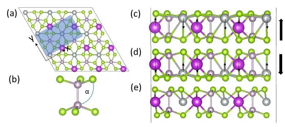
Fig. 1 (a) Top and (b-e) side views of monolayer ABP2X6(A = Ag, Cu; B = Bi, In; X = S, Se) in 3 × 3 × 1 supercell lattice structure in honeycomb unit cell.The purple, green, grey, and pink balls represent B, X, A, and P atoms, respectively.The rectangular blue shade displays the unit-cell adopted for the calculation of mechanical property, which contains two ABP2X6 formula units in Fig. 1a.Fig. 1b presents the PX3-PX3 configuration, with the angle being α between P-P bond and X atoms. Color online.
Fig. 1 presents the top view (Fig. 1a) and side views (Fig.1c-e) structures of single layer of monolayer ABP2X6, which consists of two layers of X atoms, with A, B and P-P atoms sitting between X layers forming an angle of α (Fig. 1b). A+and B3+ions in ABP2X6shift to opposite directions with different displacements to form the anti-ferroelectric distortion mode (Fig. 1c-d). The A+ion off-center along z direction is much greater than that of the B3+ion (Fig. 1c). A spontaneous polarization is generated vertical to the layers, resulting in a FE ordering, denoting as P ↑ (Fig. 1c), which is the most stable state. When B3+ion is predominantly in the upper site, and the A+ion is slightly displaced downward from the octahedral center, the polarization turning over, denoting as P ↓ (Fig. 1d).If the two off-center A-B sites are equally aligned, this would lead to the appearance of the paraelectric state (Fig. 1e). Here taking ABP2X6(A = Ag, Cu; B = Bi, In; X = S, Se) for example, the lattice parameters and out-of-plane FE polarization are 0.658 nm, 4.2 × 10⁻¹²C·m-1for CuInP2S6,0.659 nm, 3.09 × 10⁻¹²C·m-1for CuBiP2Se6, 0.640 nm, 2.37 ×10⁻¹²C·m-1for AgBiP2S6, and 0.669 nm, 1.71 × 10⁻¹²C·m-1for AgBiP2Se6 (0.675 nm and 1.20 × 10⁻¹²C·m-1)21,respectively.
Having investigated the structure of ABP2X6(A = Ag, Cu;B = Bi, In; X = S, Se) monolayers, we next study their electric properties. Fig. 2 gives the band structure of monolayer ABP2X6 calculated by PBE (black line) and HSE (red line)methods, respectively. Indirect bandgaps are predicted along high symmetry path in the first Brillouin zone by adopting the honeycomb lattice unit cell (Fig. 2a-d), and PBE gives smaller value for bandgap compared with HSE methods34-38. PBE gives bandgaps of 1.63, 1.29, 2.25, and 1.48 eV for CuInP2S6,CuBiP2Se6, AgBiP2S6, and AgBiP2Se6 (1.47 eV21),respectively, while HSE method estimates larger values, which are 2.73, 2.17, 3.00, and 2.31 eV for CuInP2Se6, CuBiP2Se6,AgBiP2S6, and AgBiP2Se6(2.31 eV21), respectively. Thus,monolayers ABP2X6are semiconductors, which might be ideal photocatalyst21. Also,we found that the main contributions of the CBM are p orbitals of X and B atoms, while the VBM is due to the hybridization of p orbital of X atoms and d orbital of A atoms (Fig. 2e). Considering that there are three short and three long A/B-X bonds due to the A-B off-center displacement, together with the d-p orbital hybridization, it is expected that the main reason for the distorted FE structure in ABP2X6 monolayers is the Jahn-Teller effect39. Given the particular structure of monolayers ABP2X6 (A = Ag, Cu; B =Bi, In; X = S, Se), it can be assumed that they might exhibit novel mechanical properties. To probe the mechanical properties of monolayer ABP2X6, we apply uniaxial strain in x and y (Fig. 3) directions, respectively. And we found that there is a phase transition between FE and paraelectric under uniaxial strain of approximately 10% along x or 13% along y for monolayer ABP2X6.Thus, we constraint our uniaxial strain within -5% to +5% in x (εx) and y (εy) (Fig. 3) directions,respectively to investigate its mechanical property. The inplane changes x with y or y with x are identical for monolayer ABP2X6, and the lattice parameter along x decreases with the increasing of strain along y, and vice versa. The values of positive Poisson’s ratio along x (νx) and along y (νy) are almost the same, indicating its in-plane isotropy mechanical behaviour (black lines in Fig. 3). For the out-of-plane direction, under compressive strain, the buckling height decreases with the increasing strain (red lines in Fig. 3),however, when it comes to tensile strain, it presents NPR for both directions (blue lines marked by cyan ellipses in Fig. 3).Remarkably, the out-of-plane NPR values for ABP2X6monolayers in both x- and y-directions are quite high compared with black phosphorous (-0.027)4, borophene (-0.04)9, and SnSe (-0.17)6. Comparing the NPR values along y direction(AgBiP2S6(-0.805) < AgBiP2Se6(-0.778) < CuBiP2Se6(-0.670) < CuInP2S6 (-0.060)), we can draw an interesting conclusion that the heavier A, B atoms are and the lighter X atoms are, the more obvious NPR effect can be acquired.This is in consistent with a general belief that the values of the Poisson’s ratio (ν) for covalent materials are smaller than the metallic materials. In this case, monolayer AgBiP2S6has the largest absolute Poisson’s value, indicating an increase of metal-metal bonding when the d-orbital metal goes from group IIB (In) to group VB (Bi) and from Cu to Ag.
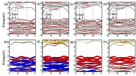
Fig. 2 Calculated band structure of monolayer ABP2X6 in a honeycomb lattice unit-cell with PBE (black line) and HSE methods (red line).(a-d) Band structures of CuInP2S6, CuBiP2Se6, AgBiP2S6, and AgBiP2Se6, respectively. (e-h) Orbital resolved band structure of CuInP2S6, CuBiP2Se6,AgBiP2S6, and AgBiP2Se6 monolayer. The CBM is contributed by s/p orbital of In/Bi atom (green/yellow) and Se atom (red), and VBM is contributed by the hybridization of p orbital of Se (red) and d orbital of Ag/Cu atom (blue). The Fermi level is set at the energy zero point. Color online.
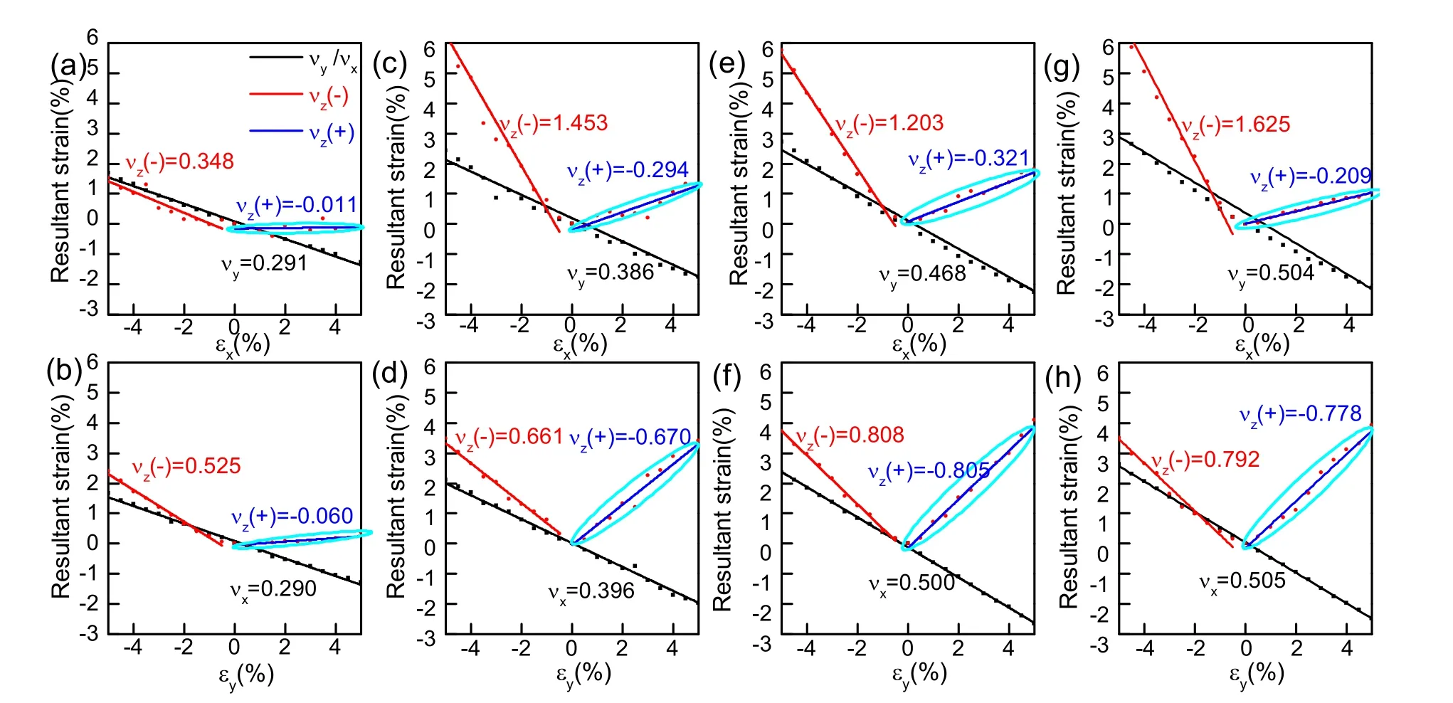
Fig. 3 Poisson’s ratios for CuInP2S6 (a-b), CuBiP2Se6 (c-d), AgBiP2S6 (e-f), and AgBiP2Se6 (g-h) as a function of strain applied along the x and y axes (-5% - 5%).The axes x, y, and z correspond to the in-plane lateral and thickness directions, respectively. The black lines represent the in-plane Poisson’s ratio. The red lines represent out-of plane Poisson’s ratio under compressive strain, and the blue lines marked by cyan ellipses represent NPR along out-of plane direction under tensile strain. Color online.
Then we move to investigate the origin of the NPR from the mechanical aspect. Taking monolayer AgBiP2Se6as an example, when tensile (+5%) or compressive (-5%) strain is applied along y direction, the lattice parameter along x decreases (a = 1.129 nm) or increases significantly (a = 1.188 nm) compared with that of strain-free lattice parameter (a0=1.158 nm). Both tensile and compressive strain effectively affect the pucker of single-layer AgBiP2Se6sheets, which enlarge the angle α (Fig. 1b) between pillar like P-P bonds and top layer Se atom, from 105.29° to 106.92°/105.71°. This corresponds to the increase of the buckling height, from strainfree buckling height t0= 0.359 nm to t = 0.374 nm/0.373 nm under +5% or -5% strain. Thus, when external operations are exerted to monolayer AgBiP2Se6, tensile strain or compressive strain, they will significantly increase the buckling height,which refers to positive Poisson’s ratio for compressive strain,while for tensile strain it leads to out-of-plane NPR.
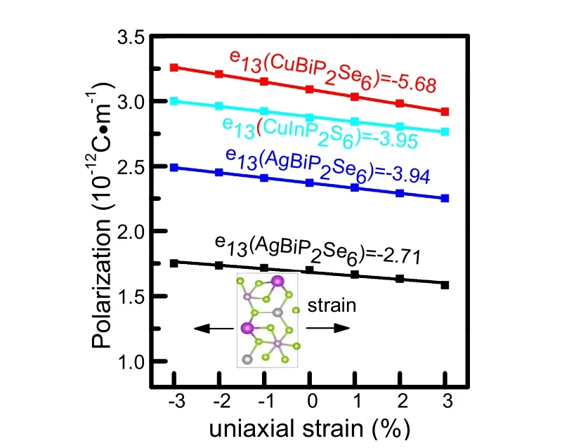
Fig. 4 Linear changes in out-of plane polarizations of the CuInP2S6,CuBiP2Se6, AgBiP2S6, and AgBiP2Se6 monolayer under uniaxial strain(y) between -3% and 3%, giving its e13 values (unit: 10-12 C·m-1).The inset shows top view of the rectangular unit cell structure of ABP2X6 monolayer.
Considering that external strain would generate significant structural changes, the off-center displacement between A and B atoms should be affected, which would alter the ferroelectric polarization subsequently. Thus piezoelectric effect is expected to occur, which couples the electrical polarization(Pi) and strain (εjk) tensor described by third-rank tensors eijk =∂Pi/∂εjk, where i, j, and k correspond to the x, y, and z directions40.Then we study the changes of polarization under strain base on DFT calculations. Taking monolayer AgBiP2Se6as an example, uniaxial strain is applied along the y direction up to 3% and the polarization is estimated by using the Berry-phase method33. Fig. 4 presents out-of-plane polarization changes with the uniaxial strain along y direction. The value of e13 for CuInP2S6, CuBiP2Se6, AgBiP2S6, AgBiP2Se6monolayer are calculated to be -3.95 × 10⁻¹², -5.68 × 10⁻¹², -3.94 × 10⁻¹²,-2.71 × 10⁻¹²C·m-1, which are comparable to the only experimentally confirmed 2D out-of-plane piezoelectric Janus system (piezoelectric coefficient -3.8 × 10⁻¹²C·m-1)41,42. The out-of-plane piezoelectricity and FE in monolayer ABP2X6 can be used for circuit designs in device application.
4 Conclusions
In conclusion, we have studied the electric, mechanical, and electromechanical properties of ABP2X6 monolayers based on first-principles theory. They are wide bandgap semiconductors. In addition, ABP2X6monolayers harbour structure induced auxetic behaviour within FE phase. The auxetic effect in the puckered structure exists in both x and y directions, indicating the atoms alignment is sensitive to external strain. The uniaxial strain further affects the A-B offcenter displacement, and ABP2X6 monolayers also exhibit outof-plane piezoelectric polarizations. These findings expand the 2D out-of-plane piezoelectrics and NPR families. The superior electronic properties, along with the NPR, make monolayer ABP2X6promising materials for the design of nanoelectromechanical devices.
Acknowledgement: D.A. acknowledges the computer resources provided by high-performance computer time from computing facility at the Queensland University of Technology, NCI National Facility, and The Pawsey Supercomputing Centre through the National Computational Merit Allocation Scheme supported by the Australian Government and the Government of Western Australia.
