Design of Power Amplifier for mmWave 5G and Beyond
2019-09-25LILianmingSIJiachenCHENLinhui
LI Lianming,SI Jiachen,CHEN Linhui
1.School of Information Science and Engineering,Southeast University,Nanjing 210096,P.R.China;
2.National Mobile Communications Research Laboratory,Nanjing 210096,P.R.China;
3.Purple Mountain Laboratories,Nanjing 211100,P.R.China
Abstract: With targets of cost reduction per bit and high energy efficiency,5G and beyond call for innovation in the mmWave transmitter architecture and the power amplifier(PA)circuit. To illustrate these points,this paper firstly explains the benefits and design implications of the hybrid beamforming structure in terms of the mmWave spectrum characteristics,energy efficiency,data rate,communication capacity,coverage and implementation technology choices. Then after reviewing the techniques to improve the power amplifier(PA)output power and efficiency,the design considerations and test results of 60 GHz and 90 GHz mmWave PAs in bulk complementary metal oxide semiconductor(CMOS)process are shown.
Key words: 5G and beyond; 6G; beamforming; complementary metal oxide semiconductor (CMOS); mmWave;multiple-input multiple-output (MIMO);power amplifier;transmitter
0 Introduction
With abundant spectrum advantage over sub-6 GHz,mmWave communication becomes a key enabler for 5G communication[1]. Recently,several licensed and unlicensed 5G mmWave candidate spectra(from 24 GHz to 86 GHz)have been selected by WRC-15 and federal communications commission(FCC),moving forward the 5G mmWave commercial deployment progress[2-4]. With wide bandwidth,mmWave 5G communication system can support more than 20 Gb/s peak data rate,which is 1 000 times that of existing 3G/4G systems. Recently,for 6G communication applications,to achieve more than 100 Gb/s data rate,it is very important to make exploitation on W-band and even higher frequency spectra,e.g. IEEE 802.15.3d-2017 252—322 GHz,which have even wider bandwidth. Note the wavelength of the W-band and beyond is very short,and these spectra can be used for the radar sensing applications,paving a way to realize the flexible joint communication and radar system[5].
However,different from sub-6 GHz band,due to very high operating frequency,the propagation loss of the mmWave band is large. To have enough communication coverage,it is very crucial for the transmitter and receiver to realize high radiated output power and sensitivity,respectively. Accordingly,the main challenge for the mmWave system is the design of the air interface,including the power amplifier(PA)as it plays an important role in the system performance,such as power consumption,efficiency and battery life[6]. To solve these issues,the phased array beamforming techniques are proposed[7]. With help of silicon and advanced packaging process,the high integrated,low cost RF front-end circuit and very compact antenna-in-package(AIP)antenna array can be realized. In this way,it is very suitable to realize mmWave system with multiple-input multiple-output(MIMO) and beamforming techniques[7-10],in particular in term of the portable handset and small cell infrastructure applications.
To date,several fully integrated mmWave communication systems have been realized using complementary metal oxide semiconductor(CMOS) process. In Ref.[11],with a 28 nm CMOS LG demonstrated a single-polarization radio frequency integrated circuit (RFIC) for smart phone applications. With 2×4 patch antenna,the system achieves 24 dBm equivalent isotropic radiated power(EIRP)and 7.5 dB noise figure. In Refs.[12-13],Qualcomm realized a 24-channel 28 GHz dual-polarization phased-array transceiver in a 28 nm CMOS process for 5G user and base station applications. With RF/IF frequency conversion,the system can support 12 antennas with two MIMO layers. The radiated pattern measurement has been undertaken,showing the 64QAM modulation spectrum and beamforming performance. However,to meet 5G key targets of cost reduction per bit and 100 times energy efficiency improvement,the system performance including the power consumption should be improved further.
The above issues call for innovations in the mmWave transmitter system architecture and the PA circuit as the PA typically dominates system power consumption. In this paper,after highlighting the characteristics of mmWave spectrum,the system architecture and technology implementation choices are discussed. Then the techniques to improve the PA output power and efficiency are reviewed. Moreover,a 60 GHz PA and a 90 GHz W-band PA are realized in 65 nm and 40 nm CMOS processes,respectively,and their results are shown.At the end of this paper the conclusion is shown.
1 mmWave Communication System Architecture and Technology Choice
1.1 mmWave spectrum characteristics
Fig.1 shows the spectrum for sub-6 GHzand mmWave communication applications. Clearly,compared with the crowded sub-6 GHz band,the spectrum beyond 24 GHz has the feature of broad bandwidth,making it possible to realize high speed throughput in 5G new radio(NR)and future 6G applications. In WRC-15 conference,several 5G candidate high frequency bands are selected,including 24.25—27.5,31.8—33.4,37—43.5,45.5—50.2,50.4—52.6,66—76 and 81—86 GHz. Recently US FCC announced several licensed and unlicensed mmWave spectrums, i. e. 28 GHz (27.5—28.35 GHz),38 GHz (37—40 GHz),64—71 GHz[3].

Fig.1 Available spectrum for the wireless communication
Fig. 2 shows the free space propagation loss ch-aracteristics of the high frequency bands. Basically,the free-space path loss is proportional to square of link distance and carrier frequency. On top of that,the oxygen and water absorption give an extra loss. On the other hand,the mmWave band wavelength is very small,and it is susceptible to blockage[7].
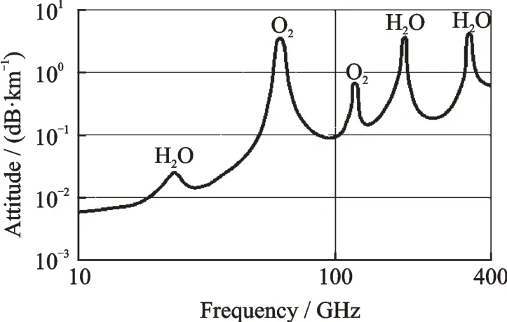
Fig.2 Free space propagation loss
1.2 System architecture
Due to the above unique characteristics of the mmWave band,to meet 10—200 m coverage and to improve system speed,energy efficiency and spectrum efficiency,the RF transceiver is typically realized by the hybrid beamforming architecture,as shown in Fig.3. In this architecture,each channel consists of PA,LNA,RF phase shifter(PS),etc.Different from LO-path, baseband, and digital beamforming architecture[14-19],with the RF beamforming architecture the transmitter/receiver chain is shared,and the interference can be suppressed,leading to very compact footprint layout and high linearity performance.
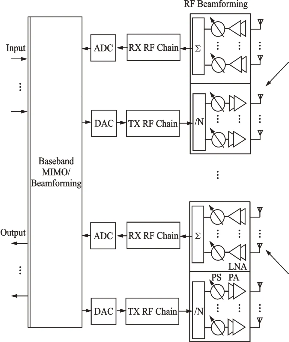
Fig.3 Hybrid beamforming architecture
From the implementation and operating perspective,this architecture can be viewed as a combination of the MIMO and beamforming techniques[7],and has following advantages:(1)The high directivity and beam scanning can be achieved with the antenna array. Accordingly,for a certain EIRP,the requirements on each RF front-end component,like the antenna gain and the PA output power,can be relaxed,thereby reducing the system power consumption and increasing the system energy efficiency.(2)With high beam directivity and large path loss of the mmWave band,the signal spatial isolation is improved,and the frequency can be reused through small cell techniques,making it possible to suppress the interference and simultaneously accommodate many co-channel users. In this way,the mmWave system spectrum efficiency and capacity are enhanced substantially.(3)In the 4G LTE MIMO system,each antenna has its own transmitter/receiver chain, including RF, IF, analog front-end,PLL,AD/DA and baseband parts. For 5G systems,with very large channel bandwidth and high operating frequency,these elements are typically the bottleneck of the system and consume a lot of DC power. With the hybrid beamforming architecture,these elements are shared by each antenna sub-array,thereby simplifying the system complexity and improving power efficiency.
As an important part of the system,the waveform has a very large impact on 5G operation. In particular,on top of the wide bandwidth,to increase the throughput further,high order modulation schemes will be employed. As shown in Fig.4,accordingly to 3GPP R15 standard,the OFDM 256QAM modulation with 10.5 dB peak-to-average power ratio(PAPR)will be used[8]. To achieve longer battery life,such high PAPR places stringent power added efficiency(PAE)and linearity requirements on the PA. Note to meet the system error vector magnitude(EVM)requirements,typically the PA needs to work at the back-off mode.
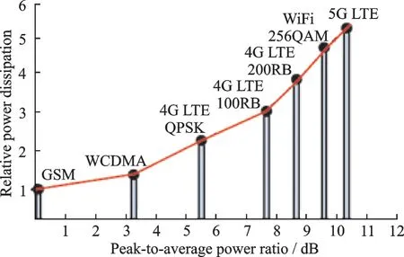
Fig.4 Peak-to-average power ratio (PAPR)[8]
2 Technology Choice
Considering the future mass consumer market requirements, it is very critical to realize the mmWave system in a cost-effective and energy-efficient way,which strongly depends on the implementation technology and antenna array size.
To illustrate this issue,a link budget calculation is undertaken. As shown in Fig.5,to achieve 60 dBm EIRP,there is a clear trade-off between the antenna array size and each PA output power[9].When GaN and GaAs are used,the antenna size can be reduced to be 100 or less. In contrast,when silicon process,like SiGe and CMOS,is used,the antenna size has to be larger than 100. Considering the antenna array working mechanism,the former solution can realize wide beams,which is very good for the mobility applications[10]. On the other hand,it can also be used to realize long coverage if the antenna size is increased.With silicon process,the system integration level can be improved and cost can be reduced. Because of this reason,both academia and industry put a lot of efforts on the research of the fully integrated silicon mmWave RF transceiver[11-18]. Note the disadvantage of large antenna size is that the beam is relatively narrow,making the beamforming phase error very critical. Accordingly,the on-chip calibration becomes indispensable.
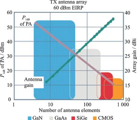
Fig.5 Trade-off between the antenna gain and PA output power[9]
3 PA Circuit Topology to Enhance Output Power and Efficiency
With above discussion,it can be clearly seen that the PA output power and power efficiency are very critical for the system coverage and power dissipation. In this part,the state-of-the-art implementation schemes of the mmWave PA will be reviewed,in particular in terms of CMOS silicon process. After that,the design considerations and test results of two mmWave PAs will be shown.
3.1 Output power enhancement techniques
With the Moore law transistor size scaling,the transistor speed is enhanced,but its supply voltage is reduced as well for the voltage stress reliability issues. With a certain impedance level,this means that the output power of the PA is reduced. To achieve a large coverage with small antenna size,the stacked FET based PA[20-21]and power combining[22]techniques can be used to increase the PA output power.
To solve the above mentioned reliability issues,as shown in Fig.6,a stack FET based PA structure is proposed using the SOI process,in which multiple devices are connected in series[20-21].Different from the typical Cascode amplifier topology,in this structure the same current is shared and the voltage swing is distributed equally across the transistor terminals. In other words,the impedances seen by each transistor drain (Zs1,Zs2and Zs3)should increase with a suitable step from bottom to up. Note to meet such requirements,special attentions should be paid to the sizing of the gate termination capacitor C2and C3.
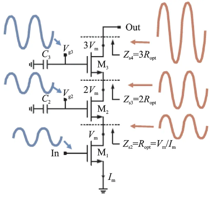
Fig.6 Stacked FET based PA structure[21]
Instead of the above voltage mode operation,as an alternative solution,as shown in Fig.7,in 2010 the transformer based power combining technique was introduced for mmWave PA using a bulk CMOS process[22]. To increase the output power,with the distributed active transformer two unit differential amplifiers are combined in the current domain. In this way,the output power is enhanced without harming the transistor reliability. In this design the slow wave and inductor source degeneration techniques are used for the passive element insertion loss reduction and PA linearization,respectively.
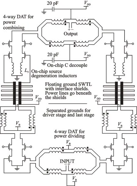
Fig.7 Transformer based power combining PA structure[22]
3.2 Output efficiency enhancement techniques
As mentioned above,the high order modulation scheme,such as 64QAM,has a very large PAPR,and the PA has low back-off PAE efficiency.To solve these issues,the Doherty PA can be used,as it has high efficiency over a large signal range[23].
As shown in Fig.8,two amplifiers are in parallel and work in the class-AB and class-C mode,respectively. With the transformer,these two amplifiers,the main and auxiliary amplifier,are combined together[24],leading to a Doherty amplifier operation. In Ref.[24],to solve the efficiency reduction due to the parasitic capacitance of the non-operational amplifier,a tuning network including Ltuneand Cseris introduced. When the amplifier is in the back-off mode,it tunes out the parasitic capacitance of the auxiliary amplifier. When both amplifiers are active,this tuning network realizes an impedance down conversion,resulting in a lower impedance for the auxiliary amplifier than that of the main amplifier. In this way,both the peak output power and back-off efficiency are improved.
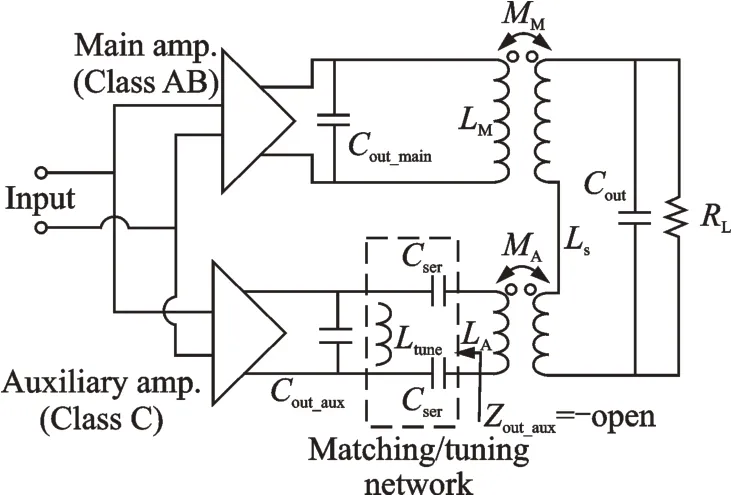
Fig.8 Transformer-based Doherty power amplifier for mmwave applications[24]
With the transformer and the digital control techniques,a digital control switching PA technique can be realized with reconfiguration of several sub-PA blocks,as shown in Fig.9.Depending on requirements on the back-off power,the switches(SW2,SW3and SW4)are switched on or off. With the power combining transformer,several efficiency peaks can be realized,enhancing PAE at the deep back-off[25].
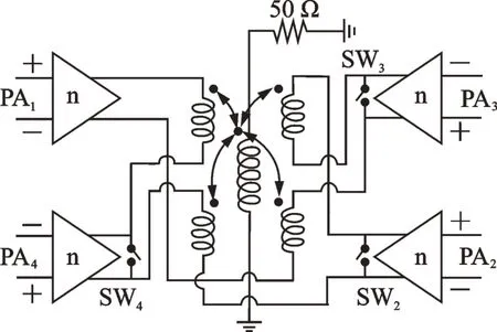
Fig.9 Digital control switching PA[25]
4 60 GHz CMOS PA with Four-Way Power Combining
Following the strategy of the power combining,with a 4-way power combing transformer,a 60 GHz power amplifier is realized in a 65 nm bulk CMOS process[26].
As shown in Fig.10,the proposed PA consists of three pseudo-differential gain stages,in which the gain and stability of each stage is increased by the capacitive neutralization techniques. With thick metal layers,the transformer is implemented for lower insertion loss. However,due to the impedance mismatch it is found that inter-stage matching has a relative large insertion loss. To solve these issues,a new inter-stage impedance matching network is proposed by introducing a shunt inductor in between the second and third gain stages,whose layout and equivalent circuits are depicted in Fig.11. Clearly,this impedance matching network consists of a transformer,transmission lines and a shunt inductor.With simulations,it is proved that the insertion loss of inter-stage matching network is improved by more than 1.5 dB. In this way,the PA gain and PAE can be improved.
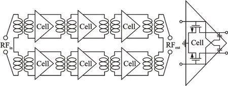
Fig.10 60 GHz PA with 4-way power-combining
This PA is implemented in a 65 nm bulk CMOS process,and its chip micrograph is shown in Fig.12. The PA core area is only about 0.6 mm2.Fig.13 illustrates the measured and simulated S-parameters across 50—70 GHz. With the help of the proposed inter-stage matching network,the measured S21is greater than 20 dB from 54 GHz to 65 GHz,with a peak power gain of 24 dB at 61 GHz. From Fig.14,under 1.2 V supply the PA saturated output power Psatand P1dBare 19 dBm and 15.4 dBm,respectively. Moreover,its peak PAE is 15.1%. With 1 V supply,Psat,P1dBand PAE are 18 dBm,14.8 dBm and 13.2%,respectively.

Fig.11 Inter-stage matching network and its equivalent circuits
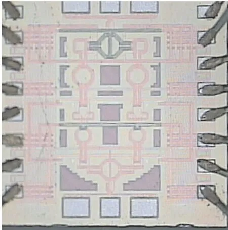
Fig.12 Micrograph of the PA
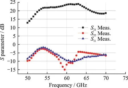
Fig.13 Measured S-parameter across 50—70 GHz
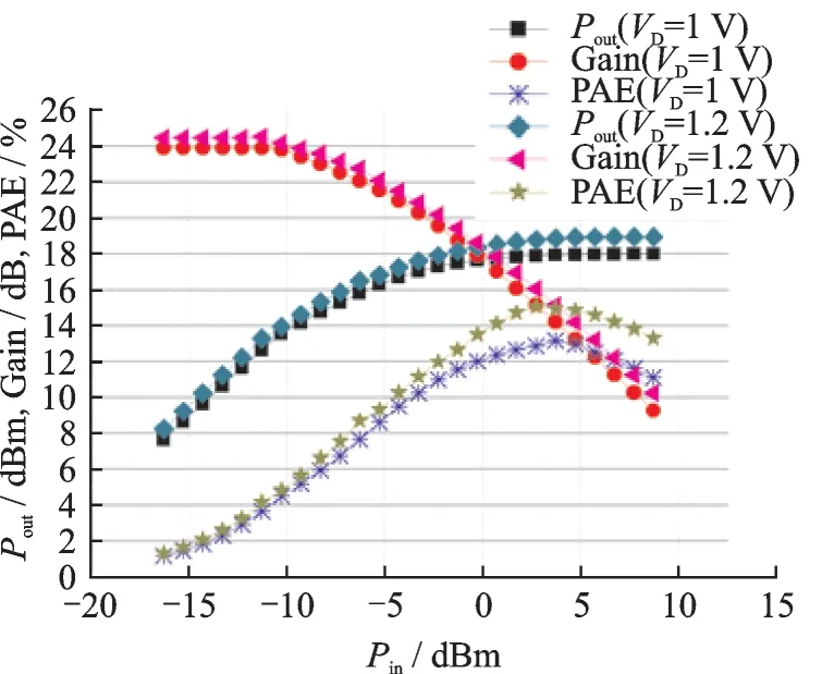
Fig.14 Measured Pout and PAE vs.input power at 61 GHz
5 90 GHz CMOS PA with Two Four-Way Power Combining
As mentioned before,for the future joint communication and radar application,it is preferred to use W-band(e. g. 90 GHz)and beyond spectra.Compared with 60 GHz operating frequency,the 90 GHz working frequency is even higher,and more advanced technology should be used. However,due to the reliability issue the supply voltage of the advanced technology is lower. These issues make it very challenging to realize a 90 GHz PA with high output power.
To solve these issues,with a 40 nm bulk CMOS process a two four-way power combining technique is used to realize a 90 GHz PA[27]. As shown in Fig.15,to achieve high output power four unit differential amplifier cells are employed,and the parallel and series power combining techniques are used to realize an efficient power combining.Taking into account the passive matching loss,the power gain of each gain stage is about 6—8 dB,and two cascading gain stages are used to provide sufficient gain. In principle,the PA output power and gain strongly depends on the transistor size. Therefore,in this design the PA output power 1 dB compression point OP1dBand power gain are optimized in terms of the transistor size. As shown in Fig.16,the PA output power can be increased by increasing the transistor size,but its power gain is reduced significantly due to the larger parasitic resistance and inductance. In this design,the transistor size of the output stage is set to be 176 μm[27]. With a loadpull simulation,it is found the PA output stage achieves 8.5 dB power gain and 11-dBm OP1dBwith a load impedance of 9.1+10.5j Ω.
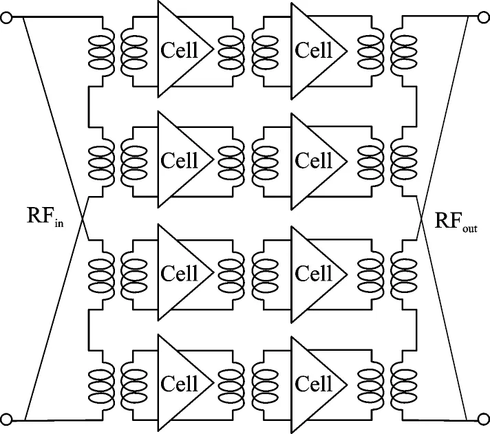
Fig.15 90-GHz PA with eight-way power combining
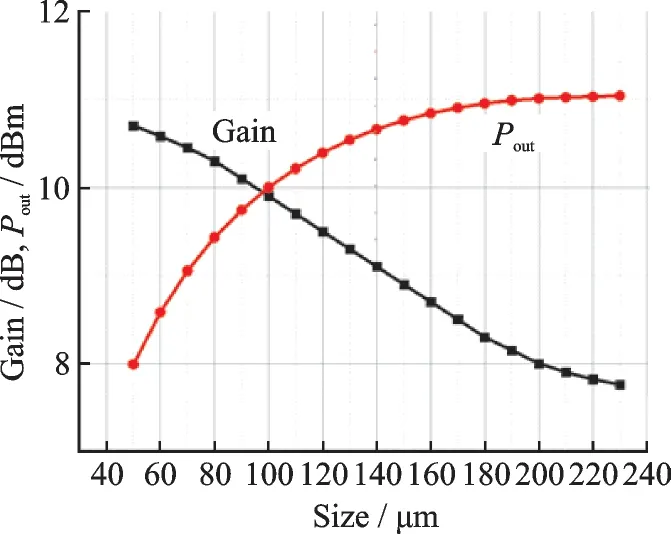
Fig.16 OP1dB and power gain versus the transistor size
A cascading PA budget calculation is undertaken to find the first stage amplifier size and increase PA power efficiency, shown as

where G(PA2)denotes power gain of the output stage;OP1dB(PA),OP1dB(PA2),OP1dB(PA1)represent 1 dB compression output power of the whole PA,the PA output stage,and the first stage of the PA,respectively. With a 8.5 dB gain of the output stage and 2 dB insertion loss of the inter-stage matching network,G(PA2)is about 6.5 dB. Assuming the transistors have the same drain efficiency,with above formula and simulations,the maximum drain efficiency and output power is achieved when the first stage size is set to be 88 μm.
Fig.17 shows the proposed two four-way transformer-based power combiners. With optimization,the radius of the transformer is set to be 28 μm. In particular,the currents from the two transformers are combined and connected to the output groundsignal-ground(GSG)pads through parallel connection metal wires. These two parallel metal wires work as inductance,realizing the impedance matching between the 50 Ω pads and transformer output.Simulations indicate that the insertion loss of the output impedance matching network is about 1 dB,preserving the PA PAE performance.
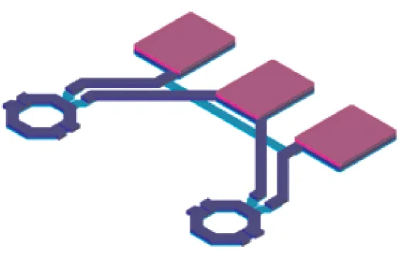
Fig.17 Output-stage matching network layout
Fig.18 shows the 90 GHz CMOS PA chip photo,and its core chip area is about 0.3 mm2. Fig.19 compares the S-parameter simulation and measurement results. Clearly,the measured S21is above 13 dB from 75 GHz to 90 GHz,with a peak gain of 14 dB at 90 GHz. The S11/S22is smaller than-10 dB across 75 GHz to 90 GHz. Note that due to measurement setup limitation,the performance beyond 90 GHz cannot be measured. As shown in Fig.20,under 1 V supply,the PA OP1dBis about 13 dBm at 90 GHz. Psat,PAE and bandwidth performance are also shown.
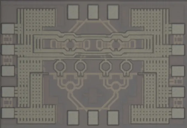
Fig.18 Micrograph of thePA
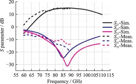
Fig.19 Measured and simulated S-parameters versus frequency
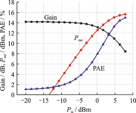
Fig.20 Measured Pout and PAE versus input power at 90 GHz
6 Conclusions
In this paper,the mmWave communication system is investigated in terms of the spectrum characteristics,implementation technology choice,PA circuit topology and design practice,system structure,etc. As an attempt to improve the PA output power and efficiency,with a 65 nm and 40 nm bulk CMOS process and the transformer based power combiner, two mmWave PAs are realized for 60 GHz communication and 90 GHz joint radar and communications applications,respectively.
杂志排行
Transactions of Nanjing University of Aeronautics and Astronautics的其它文章
- Performance Analysis and Power Allocation for Cooperative SSK System with Receive Correlation in Rayleigh Fading Channel
- Retro-reflective Beamforming Technique with Applications in Wireless Power Transmission
- A 60 GHz Phased Array System Analysis and Its Phase Shifter in a 40 nm CMOS Technology
- MoM-PO/SBR Algorithm Based on Collaborative Platform and Mixed Model
- Low-Complexity DOA Estimation of Noncircular Signals for Coprime Sensor Arrays
- A Generative Adversarial Nets Method for Monitoring Data Generation on Aircraft Engines
