Effects of active layer thickness on performance and stability of dual-active-layer amorphous InGaZnO thin-film transistors∗
2019-08-16WenxingHuo霍文星ZengxiaMei梅增霞YichengLu卢毅成ZuyinHan韩祖银RuiZhu朱锐TaoWang王涛YanxinSui隋妍心HuiliLiang梁会力andXiaolongDu杜小龙
Wenxing Huo(霍文星), Zengxia Mei(梅增霞), Yicheng Lu(卢毅成), Zuyin Han(韩祖银), Rui Zhu(朱锐),Tao Wang(王涛), Yanxin Sui(隋妍心), Huili Liang(梁会力), and Xiaolong Du(杜小龙),4,‡
1Key Laboratory for Renewable Energy,Beijing Key Laboratory for New Energy Materials and Devices,Institute of Physics,Chinese Academy of Sciences,Beijing 100190,China
2School of Physical Sciences,University of Chinese Academy of Sciences,Beijing 100049,China
3Department of Electrical and Computer Engineering,Rutgers University,94 Brett Rd,Piscataway,New Jersey 08854
4Songshan Lake Materials Laboratory,Dongguan 523808,China
Keywords: thin film transistor,InGaZnO,dual-active-layer
1. Introduction
Amorphous oxide semiconductor-based thin-film transistors (TFTs) are considered as the most prominent candidate for next-generation flexible display systems[1-3]and many other applications.[4]The TFT parameters of field-effect mobility (µFE), ON/OFF ratio, sub-threshold swing (SS), and threshold voltage (Vth) are critical for the practical applications. These parameters are strongly influenced by the oxygen vacancies in the active layer. A high-temperature(>300°C) post-annealing process is required to control the concentration of oxygen vacancies to optimize the electrical characteristics.[5-7]However, such high processing temperature is generally incompatible with many common polymer substrates. In addition,µFEand Vthshow opposite dependence on the carrier concentration: a high carrier concentration of the active layer leads to a large µFEbut a negative and poorcontrollable Vth,while a lower carrier concentration results in a positive Vthbut a much lowerµFE.[8]
Many groups have adopted the dual-active-layer (DAL)architecture to solve this contradiction and achieve high mobility and suitable Vthsimultaneously.The DAL normally contains a bottom layer with high electron concentration and a top layer with low defect density. The former is close to the channel and the latter close to the contacts. Kim et al. reported a DAL TFT with indium-zinc oxide(IZO)or indium-tin oxide(ITO)bottom layer and InGaZnO(IGZO)top layer.[8]The thin IZO or ITO layer is for the high mobility and the IGZO layer for the suitable Vth. Kim et al. proposed solution-processed AlInZnO (AIZO)/InZnO (IZO) DAL TFTs and came to a similar conclusion.[9]Marrs et al.fabricated IGZO/IZO DAL TFTs on flexible plastic substrates and demonstrated that a high saturation mobility and good gate bias stress stability could be achieved without the necessity of high-temperature annealing.[10]Many other groups studied the influence of the components of the two layers, or the thickness of the bottom layer with high carrier concentration,on the performance and stability of the devices.[11-18]
Compared with the above-mentioned hetero-DAL structures, the homo-DAL structure has a simple fabrication process. Nag et al.proposed the single-source dual-layer concept and applied it to the display and circuits.[19]Tian et al.fabricated fully transparent DAL IGZO TFTs with different oxygen compositions in two layers.[20]Park et al. studied the influence of oxygen vacancy concentrations in both IGZO layers on the device stabilities.[21]In the present study,we fabricate DAL IGZO TFTs by simply adjusting the O2/Ar gas ratio during the sputtering at 100°C without post-annealing, and investigate the effect of the thickness of both the bottom layer(low-resistance layer)and the top layer(high-resistance layer)on the TFT parameters. The dependence of positive gate bias stress stabilities and hysteresis phenomena on the thickness of each layer is explored and analyzed as well. The role of the IGZO homojunction interface was revealed based on the morphological characterization of the bottom layer and its influence on the device performance.
2. Experiment
The structure of the DAL IGZO TFTs is illustrated in Fig. 1(a). First, a 35-nm-thick Cr gate layer is deposited on quartz glass by radio frequency(RF)magnetron sputtering and patterned by UV-lithography followed by wet etching (JET-929, Changsha Jinxin Electronic Materials Co. Ltd). Then a 30-nm-thick Al2O3gate dielectric layer is deposited by atomic layer deposition(ALD)and patterned by UV-lithography and wet etching (hot dilute AZ 300MIF developer). The lowresistance (low-R) IGZO layer is prepared by RF-magnetron sputtering at 100°C with pure Ar atmosphere, followed by in situ deposition of a high-resistance(high-R)IGZO layer at 100°C with a mixed sputtering gas of Ar/O2=10:4. The DAL channel is patterned by the third-step UV-lithography and wet etching (dilute hydrochloric acid). Lastly, a 100-nm-thick ITO source/drain electrode is deposited by RF-magnetron sputtering and patterned by a lift-off method. No post-annealing treatment was conducted on the as-fabricated TFTs.
To investigate the effect of active layer thickness on the TFT performance, we first vary the growth time of low-R IGZO from 0 min to 5 min while keeping a constant 30 min growth of the high-R IGZO layer. The low-R IGZO growth time was optimized as 4 min in this case,then the high-R IGZO growth time was adjusted from 15 min to 60 min. The samples are labeled as (growth time of low-R)+(growth time of high-R). For instance, 3+30 means that the growth time of the low-R layer is 3 min and the high-R layer 30 min.

Fig.1. Schematic diagram of DAL IGZO TFT.(a)Structure from the crosssection view. (b) Micrograph from the top view. The scale bar represents 100µm.
The film thickness is measured by a surface profiler(KLA-Tencor P-6). The electrical properties are revealed using the Van der Pauw method(HMS-3000,Ecopia). The surface morphology and roughness are evaluated by atomic force microscopy(AFM;Dimension Edge,Bruker). I-V characteristic measurements are performed in the dark using a Keithley 4200 semiconductor characterization system.
The circular Corbino TFT structure can be seen in Fig. 1(b). The inner cycle with the radius R1of 252 µm is the source and the outer ring with the radius R2of 268µm the drain. The channel length (L) is given by R2-R1, whereas the effective channel width (W) is π(R1+R2). The µFEand SS are derived from the forward sweep of transfer characteristics with a drain voltage(VDS)of 0.1 V using the following equations:[3]
where Coxis the specific capacitance of the gate dielectric per unit area,IDSthe drain current,and VGSthe gate voltage. The ON/OFF ratio is defined as the absolute value of the ratio of IDSat VGS=10 V to that at VGS=-10 V for comparison.The Vthis defined as the value of VGSwhen IDS=W/L∗1 nA in the linear region. The hysteresis voltage(VH)is defined as the difference in Vthextracted from VGSsweeps between offto-on and on-to-off. All TFT parameters except for VHare obtained from three independent devices where each test is repeated three times.
3. Results and discussion
The dependence of the total active layer thickness on the low-R IGZO growth time and high-R IGZO growth time is demonstrated in Fig. 2(a) and Fig. 2(b), respectively. The growth rates are extracted from the linear fitting, which are 2.99 nm/min for low-R IGZO and 0.85 nm/min for high-R IGZO. In fact, the IGZO grows much slower under oxygenrich conditions.[22]
Figure 3 shows the surface morphology of low-R IGZO films. For the growth time of 1 min, the surface is islandlike and the root mean square (RMS) roughness is 1.60 nm,as shown in Fig. 3(a). When the growth time increases to 2 min,the islands coalesce into a smooth film with a low RMS roughness of 0.304 nm [Fig. 3(b)]. Figure 3(c) indicates that the 4 min low-R IGZO film becomes even smoother, where the RMS roughness is 0.140 nm. The smooth surface of low-R IGZO facilitates the formation of an abrupt homo-interface with high-R IGZO,which is of great importance for the electron transport.[17]

Fig.2. The dependence of total channel layer thickness on the growth time of(a)the low-R IGZO layer(with 30 min high-R IGZO layer)and(b)the high-R IGZO layer(with 4 min low-R IGZO layer).
The low-R IGZO film sputtered under oxygen-deficient conditions contains a large number of oxygen vacancies, which leads to a high electron concentration of 1.52×1019cm-3. Such a high concentration of electrons could passivate the trap states at the interface between the channel and dielectric layers effectively.[14,23]The Hall mobility of low-R IGZO is 10.4 cm2/V· s and the resistivity 3.97×10⁻²Ω· cm. The resistance of high-R IGZO film is higher than 200 MΩ and cannot be measured in the HMS-3000 Hall system.
Figure 4 shows the transfer characteristics for the IGZO TFTs with different thicknesses of low-R layers. The TFT parameters are summarized in Table 1. The 0+30 sample,i.e. the sample only containing a high-R IGZO single active layer, exhibits a very low ON/OFF ratio of about 200 and very large VHabove 9 V at VDS=0.1 V, where the on-state IDSeven decreases with elevated VGS, as shown in Fig. 4(a).The transfer curve with VDS= 5 V presents Vth>9 V and degraded IDSwith respect to that of VDS=1 V. Defects are generated at the dielectric interface during the sputtering of IGZO, which traps the electron during the VGSsweeping and leads to the low on-state IDS, large clockwise VHand nonequilibrium,non-steady-state TFT operation.[24]The ON/OFF ratio increases by two orders of magnitude after inserting a 1 min low-R IGZO layer,but theVHis still very large,as shown in Fig.4(b).The AFM image in Fig.3(a)demonstrates that the 1 min low-R IGZO is discontinuous so that the current flows partly though the low-R IGZO and partly through the high-R IGZO. A large number of defects remain at the interface between the dielectric and high-R IGZO layers, which will still trap the electrons and lead to the non-equilibrium,non-steadystate TFT operation. The 2-min low-R IGZO layer turns into continuous film,benefitting the passivation of the interface defects by the large number of electrons. The ON/OFF ratio is ∼107, even reaching 1010when the minimum and maximum currents at VDS=5 V are chosen. The VHis smaller than 0.3 V[Fig.4(c)]. Note that the Vthshifts in the negative direction with thicker low-R IGZO layer due to the increasing total number of electrons[Figs.4(c)-4(f)]. The best TFT performance belongs to the 4+30 sample, where the µFEis 5.41±0.05 cm2/V·s, SS 95.0±6.9 mV/dec, ON/OFF ratio 6.70±0.95×10⁷,Vth0.24±0.12 V,and VH0.13 V.

Fig. 3. AFM image of low-R IGZO film with the growth time of (a)1 min,(b)2 min,and(c)4 min.
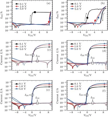
Fig.4. Transfer characteristics for IGZO TFTs with different thicknesses of low-R layers: (a)0+30,(b)1+30,(c)2+30,(d)3+30,(e)4+30,and(f)5+30.
Figure 5 manifests the output characteristics of the IGZO TFTs with various thicknesses of low-R layers. The curves do not show much difference except for the current values. The excellent saturation demonstrates the small contact resistances.

Fig.5. Output characteristics of IGZO TFTs with different thicknesses of low-R layers: (a)2+30,(b)3+30,(c)4+30,and(d)5+30.
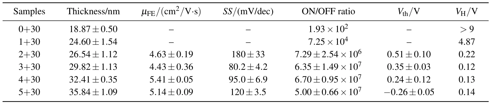
Table 1. Summary of TFT parameters for low-R IGZO layer with different thicknesses.
The transfer characteristics for the IGZO TFTs with various thicknesses of high-R IGZO layers are shown in Fig. 6.The 4+15 sample exhibits large clockwise hysteresis, which is reduced to smaller than 0.2 V for the 4+30 sample. Intriguingly,the hysteresis changes its direction from clockwise to counterclockwise for the 4+45 sample, and the counterclockwise hysteresis becomes bigger when the thickness of the high-R IGZO layer further increases. The TFT parame-ters are summarized in Table 2. The hysteresis voltage VHgradually changes from 1.47 V to -1.41 V as the thickness of the high-R IGZO increases. Generally, the counterclockwise hysteresis phenomenon is attributed to several mechanisms: (i)acceptor-like defects in the dielectric or at the channel/dielectric interface,[25,26](ii) slow polarization in the dielectric layer,[27-29](iii)mobile charges,[30,31](iv)charges injected from the gate electrode,[32-34]and (v) negative capacitance by ferroelectric dielectric,[35,36]but none of them can explain the transition trends with the thickness change of the high-R IGZO. In this case, the interface between the dielectric and channel is the same for all these samples, while the only difference is the high-R IGZO layer. The counterclockwise hysteresis has also been reported in bilayer InGaO TFTs with a 10-nm-thick front channel layer and 40-nm-thick back channel layer,[37]where the thickness of both layers is close to that of the 4+60 sample. ZnO/ZnMgO field-effect transistors with two-dimensional electron gas in the ZnO channel also exhibit counterclockwise hysteresis.[38]The existence of a large amount of carriers in the channel might be the origin of the hysteresis phenomenon. The mechanism needs to be further investigated.
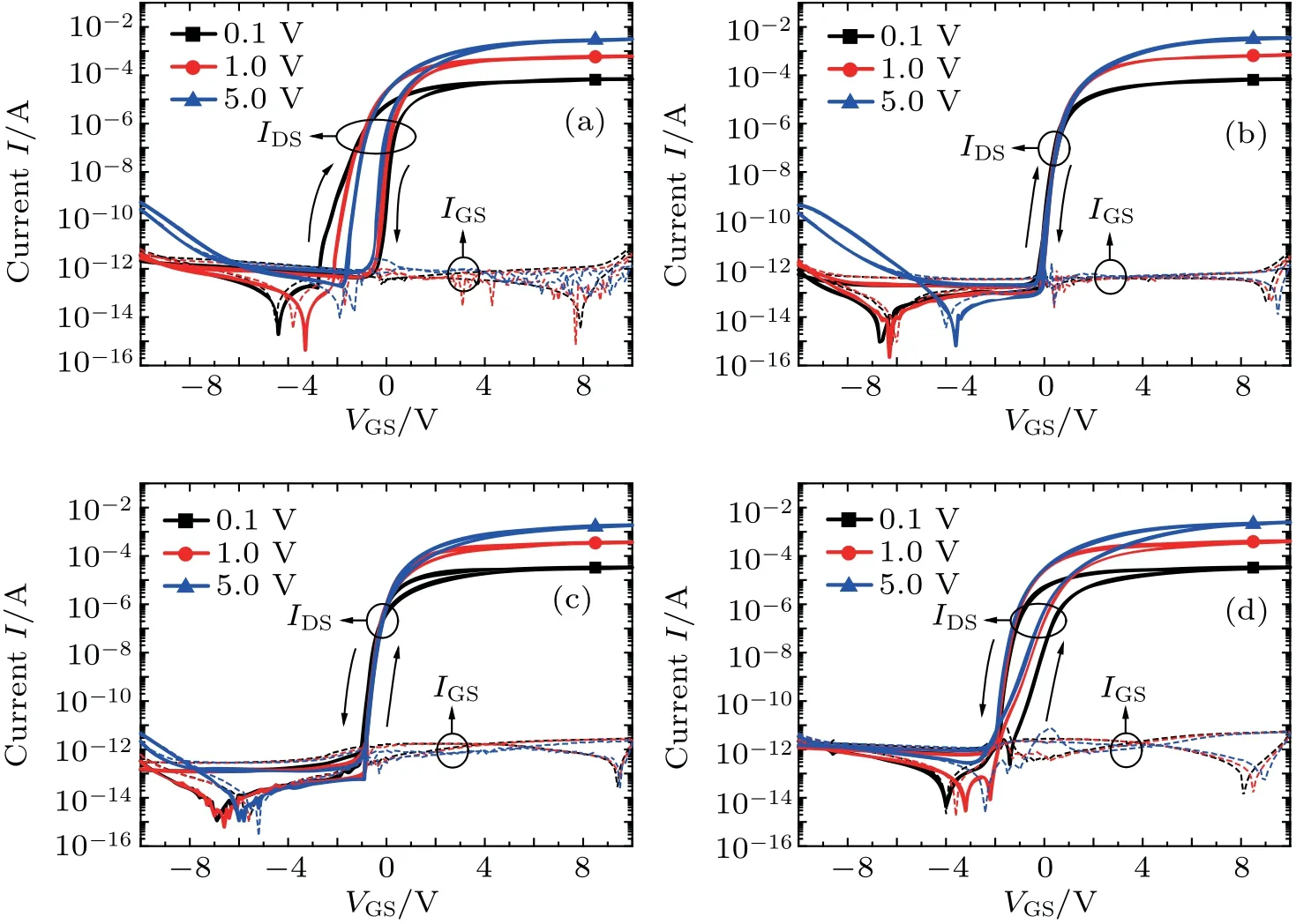
Fig.6. Transfer characteristics for IGZO TFTs with different thicknesses of high-R layers: (a)4+15,(b)4+30,(c)4+45,and(d)4+60.
The µFEand ON/OFF ratio significantly decrease when the growth time of high-R IGZO is larger than 45 min. The off-state IDSat VDS=5 V also decreases as the thickness of high-R IGZO increases. The slight degradation of saturation current in Fig. 7(a) can also be seen from the transfer curves in Fig. 6(a), and it is different from the oversaturation hump phenomena.[20,39-41]The mechanism also needs to be further investigated. The degraded saturation current is recovered when the growth time of high-R IGZO increases to 30 min[Fig.7(b)]. On the other hand,the thick high-R IGZO acts as a large resistor that connects in series with the channel,resulting in the reduction ofµFEand off-state IDSas well as the contact resistance. The large contact resistance leads to the increase of pinch-off voltage,as shown in the output characteristics for the IGZO TFTs in Fig.7(c)and Fig.7(d).
The 4+30 sample presents the best TFT performance of all these samples. It is found that the thickness of low-R IGZO exerts little influence over the device performance as long as it forms a continuous and smooth film. However, the thickness of high-R IGZO has a huge impact onµFE,Vth,and VH. It was reported that the thick back channel layer(high-R layer in this work)controls the charge conductance,resulting in a suitable threshold voltage.[9]Here,we demonstrate that this layer also has a great effect on the hysteresis.
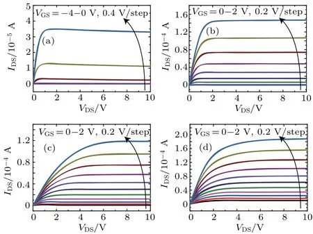
Fig.7. Output characteristics for IGZO TFTs with different thicknesses of high-R layers: (a)4+15,(b)4+30,(c)4+45,and(d)4+60.

Table 2. Summary of TFT parameters for high-R IGZO layer with different thicknesses.

Fig.8. Evolution of the transfer characteristics of IGZO TFTs for(a)2+30,(b)3+30,(c)4+30,and(d)5+30.

Fig.9. Evolution of the transfer characteristics of IGZO TFTs for(a)4+15,(b)4+30,(c)4+45,and(d)4+60.
The positive gate bias stress (PBS) characteristics of the IGZO TFTs with different thicknesses of low-R IGZO layers are shown in Fig. 8, and with different high-R IGZO layers in Fig. 9. The transfer characteristics were measured at VDS=0.1 V under a gate bias stress of VGS=10 V at set intervals. The PBS results in a positive Vthshift (ΔVth) for all samples. The value of SS is basically unchanged for all TFTs(not shown here). Therefore, the Vthshifts are dominated by the charge trapping in the gate dielectric or at the channeldielectric interface rather than on defect creation.[42-44]The threshold voltage shifts versus stress time are shown in Fig.10.The value of ΔVthdecreases with thicker low-R IGZO, as shown in Fig. 10(a). This can be attributed to the increase in the total amount of electrons,which passivates the trap states.The value of ΔVthalso decreases with thicker high-R IGZO,as shown in Fig.10(b).The dynamic interaction between the ambient atmosphere and the exposed back channel affects the Vthstability.Although there is no extra passivation layer to protect the back channel, the high-R IGZO layer serves as a passivation for the TFTs and inhibits the back channel formation.[5,44]

Fig.10.The threshold voltage shifts versus stress time with different growth times of(a)low-R IGZO layer and(b)high-R layer.
4. Conclusion
In summary, DAL IGZO TFTs with various thicknesses of both layers have been fabricated, and their effects on TFT performance and stability have been investigated.When a continuous and smooth low-R layer forms,theµFE,ON/OFF ratio,Vth,and VHare significantly improved due to the passivation of defects and the high-quality homojunction interface. The influence becomes weak after the thickness of the low-R layer increases beyond about 10 nm. The high-R layer not only affects the value of µFEand Vth, but also has a huge impact on VH. The hysteresis gradually changes from clockwise to counterclockwise with the increasing thickness of the high-R layer.The Vthshifts decrease with both a thicker low-R and high-R layer. The excellent stability of DAL IGZO TFTs facilitates their application in active-matrix liquid-crystal displays and active matrix organic light-emitting diodes.
猜你喜欢
杂志排行

Chinese Physics B的其它文章
- Lorentz transmission electron microscopy for magnetic skyrmions imaging∗
- Spin transport in antiferromagnetic insulators∗
- First-principles study of the band gap tuning and doping control in CdSexTe1-x alloy for high efficiency solar cell∗
- Non-Stokes drag coefficient in single-particle electrophoresis:New insights on a classical problem
- SymTopo: An automatic tool for calculating topological properties of nonmagnetic crystalline materials∗
- Tunable coupling between Xmon qubit and coplanar waveguide resonator∗