Electronic and magnetic properties of CrI3 nanoribbons and nanotubes∗
2019-08-06JiZhangWang王吉章JianQiHuang黄建啟YaNingWang王雅宁
Ji-Zhang Wang(王吉章), Jian-Qi Huang(黄建啟), Ya-Ning Wang(王雅宁),
Teng Yang(杨腾)1,†, and Zhi-Dong Zhang(张志东)1
1Shenyang National Laboratory for Materials Science,Institute of Metal Research,Chinese Academy of Sciences,Shenyang 110016,China
2School of Materials Science and Engineering,University of Science and Technology of China,Shenyang 110016,China
Keywords: CrI3,nanoribbon,nanotube,magnetism
1. Introduction
Two-dimensional (2D) van der Waals crystals have attracted broad attention due to their novel properties and potential applications in the last two decades.[1]The excellent mechanical,[2]electronic,[1,3-5]optical,[6-8]and especially magnetic properties[9]due to the quantum confinement effect have been widely reported. Isotropic long-range ferromagnetic(FM)order at low dimension has been proved to be thermodynamically unstable in Heisenberg systems from the Mermin-Wagner theorem.[10]However,a number of magnetic 2D-layered structures, such as FePS3,[11]Cr2Ge2Te6,[12-14]and CrI3,[15,16]have recently been demonstrated by experiments to be stable with finite ordering temperature, largely due to the magnetic anisotropy and/or the Ising systems.[17-19]Among them, CrI3exhibits in-plane FM ordering but interlayer antiferromagnetic ordering(AFM).[15]Interestingly,the layer-dependent magnetic order can be switched by an electrical gating, for example, from an interlayer AFM ordering to ferromagnetic state between the layers in bilayer CrI3by electron doping.[20,21]Circular polarized photoluminescence has also been reported in CrI3monolayer.[22]Those findings may promise CrI3for applications in spintronics and optoelectronics.
Transforming 2D atomic-thick crystals into onedimensional structures strengthens the quantum size effect in some manner and supplies a new playground for tuning electronic properties.[23-25]Especially, ribbon width and edge configuration in ribbon structures, tube diameter and chirality in nanotubes,[26]decoration style and end-size in nanowires[23]play essential roles on determining the emergent electronic and magnetic properties, as is the case with graphene nanoribbons,[27,28]MoS2nanoribbons,[29]transition metal chalcogenides nanowires,[30-32]and phosphorene nanoribbons.[33]So it is intriguing to know how different the electronic properties one can achieve or whether it is possible to enhance the magnetic properties through edge structures when bringing CrI3down from the 2D form to its ribbon or tube counterparts. Reports have barely been found in literature on this topic except for a computation study on the edge-tunable band structure in zigzag CrI3nanoribbons by Jiang et al.[34]A more systematic and thorough exploration on the size effect on the electronic and magnetic properties of CrI3nanoribbons and nanotubes is yet to be made.
In this paper, we studied the edge configuration and size dependent electronic and magnetic properties of CrI3nanoribbons(NRs)and nanotubes(NTs)by using first-principles density functional calculations. Typical zigzag and armchair edge configurations were chosen for both ribbon and tube structures, with ribbon width ranging from 12 ˚A to 70 ˚A. Both zigzag (ZZNR) and armchair nanoribbons (ACNR) are reasonably endothermic with respect to their 2D counterparts,with ZZNR slightly more stable than ACNR. Encouragingly,the Curie temperature for both nanoribbons and nanotubes(ACNT and ZZNT), as evaluated from the energy difference between the FM and AFM states,is obviously enhanced from the CrI32D crystals. Part contribution is due to the increased spin moment,especially in the case of nanotubes in which the spin moment of Cr is increased by 4%. Iodine edge atoms are also found to contribute to the increased magnetization in the ribbons. Moreover, the band gap Egof ZZNR increases with increasing ribbon width, while in contrast, the band gap of ACNR and nanotubes (ACNT, ZZNT) decreases with increasing ribbon width and tube diameter unexpectedly. More interestingly, oscillations of band gap size and spin moment of ACNT with ribbon width were found, which may be ascribed to the quantum confinement and the crucial effect of the edges.[27]Polarized optical absorption was also calculated and found to occur in the whole Brillouin zone, due to parallel flat valence and conduction bands, which is promising for optoelectronic applications.
2. Methods
We used ab initio density functional theory with the exchange-correlation functional of Perdew, Burke, and Ernzerhof (PBE) flavor[35]as implemented in the Vienna ab initio simulation package(VASP).[36]The cut-off energy for the plane-wave basis set was set to be 350 eV. The Monkhorst-Pack scheme[37]was used to sample the Brillouin zone (BZ)over a 16×1×1 k-mesh. The energy difference threshold for electronic self-consistency was set to be 10-7eV.We used the plus U method with U =2.65 eV for the Cr atom.[38]All the structures were fully relaxed with the method of conjugate gradients[39]until the atomic force was less than 0.02 eV/˚A.The van der Waals interaction was taken into account for all the structures. The vacuum space between two neighboring slabs was set to be 15 ˚A to avoid the artificial inter-slab interactions.
To evaluate the optical absorption, the electron-photon matrix element M(c,v,k) was computed based on the Fermi golden rule to obtain the absorption probability α,
in which the electron-photon matrix element M(c,v,k)is[40-42]
where m is the carrier mass, ∈0is the dielectric constant of vacuum, I is the intensity of the incident laser, D(c,v,k)(=〈ψc(k)|∇|ψv(k)〉) is the dipole vector taking care of the photon-excited electronic transition from valence state ψv(k)to conduction state ψc(k), and P is the laser polarization.Jone vectors(1, ±i, 0)were used to simulate the circular polarization of laser.
3. Results and discussion
In the following, we shall discuss the size dependence of the electronic and magnetic properties of CrI3nanoribbons and nanotubes.
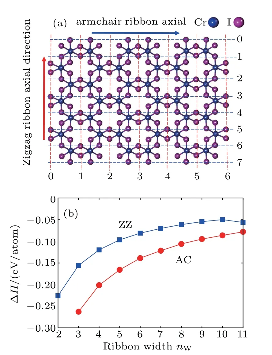
Fig.1.(a)Definition of CrI3 ribbon structures with zigzag and armchair edges. Arrows in red and blue show periodic axial directions of ZZ and AC ribbons, respectively. Dashed lines with numbers define the width index nW. (b) The nW dependence of formation enthalpy ΔH of both ZZNR and ACNR,ΔH is defined in Eqs.(3)and(4).
3.1. CrI3 nanoribbons
Let us firstly define the ribbon structures for CrI3. Two typical structures of ZZNR and ACNR are defined according to the sublattice of Cr atoms (blue), similar to the definition of graphene nanoribbon type, as shown in Fig. 1(a). Iodine atoms(purple)are selected to terminate the dangling bonds in Cr edge atoms for both types of ribbons,because it costs much more energy to have edge Cr atoms with dangling bonds from our formation enthalpy calculations. Guided by this rule, the edge structures with various ribbon widths were constructed,as highlighted in Fig. 1(a) by red and blue dashed lines and width index nWfor ZZNR and ACNR, respectively. To estimate the relative stability of ribbons with respect to the 2D CrI3crystal,the formation enthalpy ΔH for ZZNR and ACNR were calculated based on the following equations:

where ECrI3, ECr, EZZ, and EACare respectively the total energies of 2D CrI3, elementary Cr solid, ZZNR, and ACNR.Each ZZNR with width index nWconsists of 2nWCr atoms and 2+6nWI atoms, while each ACNR has 2nWCr atoms and 4+6nWI atoms.
As evident by the negative formation enthalpy given in Fig.1(b),it is always endothermic to obtain ribbon structures of any type from 2D CrI3. With decreasing ribbon width,ΔH normalized by the total number of atoms increases, suggesting that it is more difficult to get the narrower ribbon. ZZNR is more stable than ACNR at similar width, probably due to the energy gain from dimerization of the edge iodine pair in ZZNR compared with the single iodine edge atom in ACNR.
Firstly we studied the electronic properties of ZZNR,specifically the electronic band structure, magnetic properties, and relative stability between FM and AFM states, as shown in Fig. 2. The typical spin alignments of FM/AFM states are schematized in Fig 2(a), with the spin moment of Cr atoms pointing out of the structural basal plane from magnetocrystalline anisotropy calculation. The Curie temperature TCcan be estimated upon both the exchange stiffness J and saturated magnetization m according to the Weiss-Heisenberg model.[40]Exchange stiffness J can be calculated from energy difference ΔEAFM-FMbetween AFM and FM states.[43]In Figs. 2(b)-2(d), we show the ribbon-widthnormalized ΔEAFM-FMand spin moment m as a function of 1/W. As seen from Fig. 2(b), FM remains more stable than AFM regardless of the ribbon width(which is consistent with the results from Ref.[34]),and J can be increased by up to 3-4 times from 2D CrI3to ZZNR structures(width index nW≥5).Spin moment m in Fig.2(c)does not show much improvement upon the 2D counterpart.But the spin charge density ΔρFMindicated in Fig. 2(d) shows some additional contribution from the edge iodine atoms in the ZZNR (left panel) compared to the 2D crystal(right panel). It is most likely to obtain an enhancement of TCof the ribbon structures upon the bulk(61 K)and monolayer CrI3(45 K).[15,44]
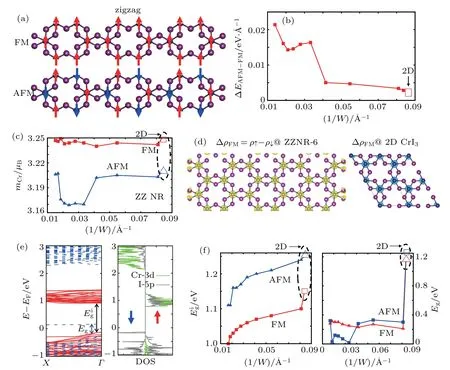
Fig.2. (a)Schematic spin alignment on Cr atoms for both FM and AFM states in ZZNR.Up arrow(red)represents spin majority and down arrow(blue)spin minority. (b)Energy difference ΔEAFM-FM (=EAFM-EFM)for ZZNR as a function of inverse ribbon width. (c)Maximal magnetic moment for Cr atoms in FM (red square) and AFM (blue triangle) states in ZZNR as a function of 1/W. (d) Spin charge density ΔρFM between spin majority and minority states for ZZNR-nW(nW=6)and 2D CrI3 with Δρ=0.118 e/Bohr-3. (e)Electronic band structure and projected density of states(PDOS)for ZZNR-6. The Cr-3d and I-5p orbitals are shown in green and gray lines,respectively. (f)Band gap of both FM and AFM states as a function of 1/W. Eig(left panel)and Eg(right panel),as defined in the band structure in(e),represent intrinsic and spin-flip band gaps,respectively.
To have more insight into the magnetic property,we calculated the electronic band structure and density of states(DOS),as showed in Fig.2(e).The projected DOS on the right panel of Fig.2(e)illustrates that not only the Cr-d orbitals(in green) but also the I-p orbitals (in grey) contribute to the net spin moment,especially the flat bands due to the I-5p orbitals near the Fermi level. The electronic instability arising from a large DOS of I-5p orbitals and the electron-electron Coulomb repulsion occurs at EF, which gives rise to a splitting of spin majority and minority bands. This is a new feature for the ribbon structures, which is not observed in the 2D counterpart.Band gap Egdue to the spin splitting, as defined in the band structure in Fig. 2(e), is about 0.2-0.3 eV (which is similar to the result in Ref. [34]), almost independent on the ribbon width, as seen from the right panel in Fig. 2(f). The optical absorption across Egshould be forbidden due to the electricdipole selection rule (Δl =±1, Δms=0), which is the case from the calculated optical absorption in Fig. 3. Meanwhile,the band gap Eigof the spin majority bands between the I-5p and Cr-4d, as defined in Fig. 2(e), should be optically active due to Δl=±1,as confirmed also in Fig.3. In contrast to the spin flip band gap Egindependent of the ribbon width,Eigincreases with decreasing ribbon width W,obviously due to the quantum size effect.
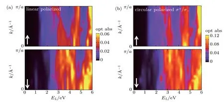
Fig.3. The optical absorption of FM ZZNR-2 with spin and momentum resolution for(a)linear polarized laser and(b)circular polarized laser.Up and down arrows in the lower left corner show majority and minority spins,respectively.
Helicity dependence of photoluminescence was reported in 2D CrI3monolayer and bilayer.[22]It is worth checking whether it exists in the one-dimensional ribbon structure. We show the wave-vector, laser-energy, and (linearly and circularly)polarization dependence of optical absorption in Fig.3.The optical gap of the spin majority band is smaller than the minority one. Due to many flat bands, the wave-vector independence of the optical absorption is obviously observed.It is a pity that no circular polarization dependence is found,namely, the helicity of both σ+and σ+gives the same result in Fig.3(b). Circular polarized laser leads to two times as big intensity as the linear polarized laser,basically due to the fact that circular polarization is due to two linearly polarized lasers with 90°phase difference.
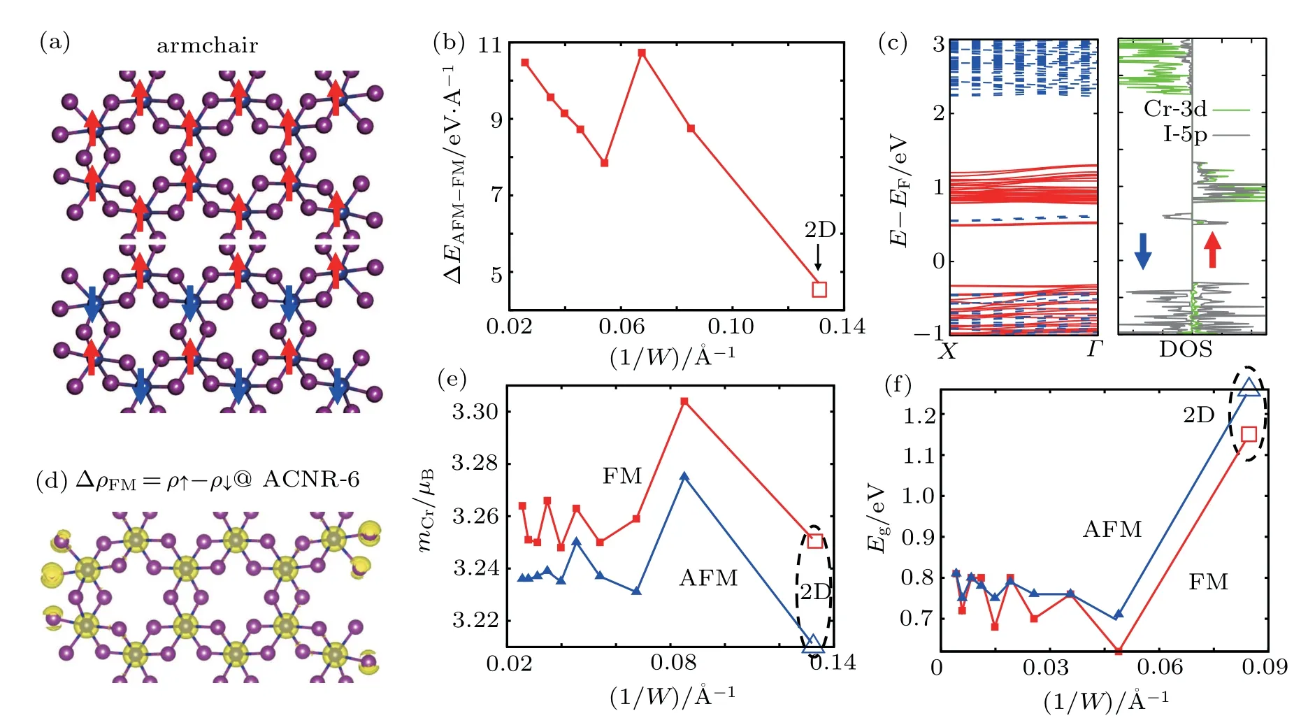
Fig. 4. Ribbon width dependence of electronic properties of ACNR. (a) FM and AFM spin alignments of Cr atoms. (b) Width normalized energy difference ΔEAFM-FM (=EAFM-EFM). (c) Band structure and projected DOS for ACNR-6. (d) Net spin charge density ΔρFM. (e)Maximal magnetic moment of Cr atoms in both FM and AFM states. (f)Band gap Eg of both FM and AFM states.
The edge type has been seen to significantly change the electronic and magnetic properties of NRs such as carbon NRs,[27]phosphorene NRs,[33]and MoS2NRs.[29]Besides the zigzag edge in honeycomb lattices, the armchair edge is another typical structure. Now let us shift from ZZNR to ACNR to see the edge structure effect on the electronic properties of nanoribbons. The spin configurations for both AFM and FM states are given in Fig. 4(a). It is encouraging to anticipate that the Curie temperature TCwill be much improved upon 2D CrI3as well in ACNR, largely thanks to the much enhanced exchange stiffness J as shown in Fig. 4(b) and slightly increased spin moment m as shown in Fig.4(e). The discussion on ACNR will, therefore, be similar to that on ZZNR. However,the oscillation of both spin moment mCrand band gap Egwith the ribbon width W is unique in ACNR, as indicated in Figs.4(e)and 4(f). Similar results have also been reported in graphene nanoribbons with armchair edge.[27]So likewise,we may ascribe such an oscillation of band gap Egas well as of m with ribbon width in the ACNR to both quantum confinement and the crucial effect of the edges.[27]
3.2. CrI3 nanotubes
Compared to ribbon structures with dangling bonds at the edge,tubular structures without edges should be more advantageous for many applications. But how about the magnetic properties in the tubular structures?Here we studied CrI3nanotubes with two typical chiralities,ZZNT(n,0)and ACNT(n,n). Figure 5(a)shows the top view and side view of two representative nanotubes,ZZNT(6,0)and ACNT(6,6). Diameter D is defined as the largest distance between two furthest iodine atoms in the cutting plane perpendicular to the tube axial direction. The strain energy is evaluated in Fig.5(b). In contrast to the weak dependence of strain energy on ribbon width in ZZNR and ACNR, the strain energy of NTs is inversely proportional to the square of the nanotube perimeter W (or diameter D),namely,E/NCr~α/D2,with α =24.03 eV·˚A2. The weak dependence of strain energy on tube chirality is very similar to that in carbon nanotubes and other tubular structures.[26]Our calculation results show that the FM state is energetic favorable compared to the NM and AFM states of CrI3NT,and the energy difference between the FM and AFM states is about 20 meV per Cr atom in CrI3NT.
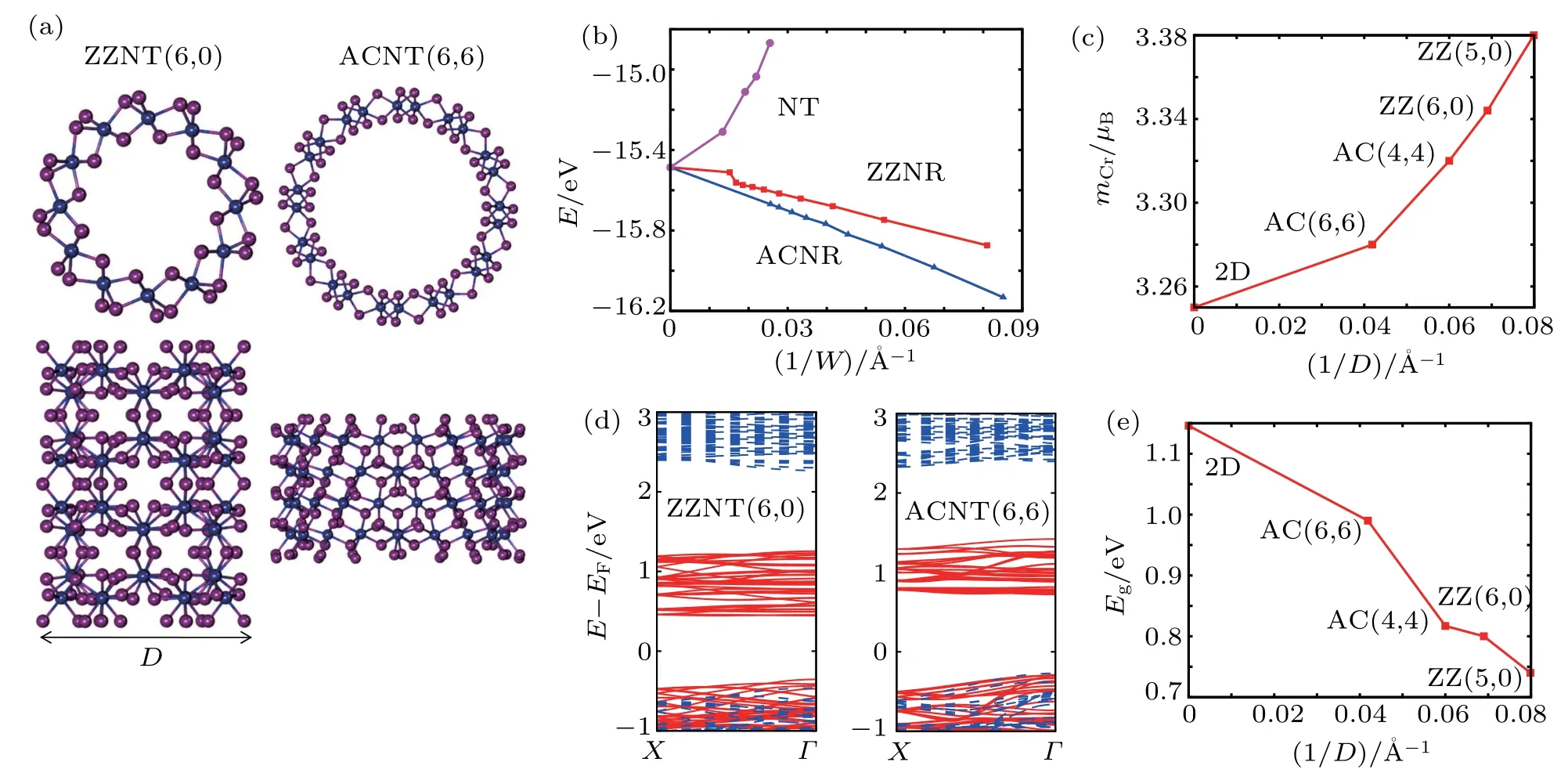
Fig.5. Tube-size dependence of electronic properties of CrI3 nanotubes. (a)Top view and side view of two chiralities(left: ZZNT(6,0)and right:ACNT(6,6)). (b) The 1/W dependence of total energy normalized by the number of Cr atoms for both nanotubes and nanoribbons. For NT,W is defined as the perimeter of the tube W =πD, with D being the diameter. (c) Maximal magnetic moment of Cr atom as a function of inverse diameter 1/D. 2D CrI3 sheet is also shown at 1/D=0. (d)Band structures for ZZNT(6,0)and ACNT(6,6). (e)Band gap as a function of 1/D.
More interestingly, the spin moment of Cr atoms mCris sensitive to the tube diameter D,as shown in Fig.5(c). The increase in mCrfrom 2D counterpart to tube is evident and about 4%can be achieved in ZZNT(5,0)(with D ~12.5 ˚A).The narrower the tube,the larger the mCr,and mCr~1/D2seems to fit well the calculation data. Such a curvature-enhanced spin moment is probably due to the distorted octahedral crystal field in the tubes. In consequence,Coulomb repulsion can surpass the crystal-field band gap Δ between the egand t2gorbitals to increase the net spin moment. Such a hypothesis can be partly confirmed from the electronic band structure. As seen from Figs. 5(d) and 5(e), the band gap Egdecreases with decreasing tube diameter D,suggesting that it becomes easier to cross the crystal field gap Δ to flip the spin when the tube becomes narrower. However,the relationship between Egand the tube size D is quite opposite to that found in carbon nanotube,[26]which needs a further study.
4. Conclusion
In summary,we have studied the structural stability,electronic properties,and magnetic properties of low-dimensional nanoribbons and nanotubes of CrI3by ab initio density functional calculations. Ferromagnetic ordering is found to be stable in all the NR and NT structures of interest. An enhancement of the Curie temperature TCcan be expected when CrI3structure goes from 2D to NR/NT. The energy difference between the FM and AFM states can be improved by even up to 3 to 4 times in ZZNR,largely because of the electronic instability arising from a large DOS of I-5p orbitals at EF. In NT structures,shrinking the tube size can reduce the crystal-field gap and drive a re-balance between spin majority and minority populations to harvest an enhancement of spin moment by up to 4%. Our theoretical results may give a guidance to the size and edge control of electronic and magnetic properties in low-dimensional magnetic devices.
杂志排行

Chinese Physics B的其它文章
- Topological magnon insulator with Dzyaloshinskii-Moriya interaction under the irradiation of light∗
- Wavelength dependence of intrinsic detection efficiency of NbN superconducting nanowire single-photon detector∗
- Artificial solid electrolyte interphase based on polyacrylonitrile for homogenous and dendrite-free deposition of lithium metal∗
- Effects of CeO2 and nano-ZrO2 agents on the crystallization behavior and mechanism of CaO-Al2O3-MgO-SiO2-based glass ceramics∗
- Modulation of magnetic and electrical properties of bilayer graphene quantum dots using rotational stacking faults∗
- Thermal conductivity characterization of ultra-thin silicon film using the ultra-fast transient hot strip method∗