Thermal conductivity characterization of ultra-thin silicon film using the ultra-fast transient hot strip method∗
2019-08-06YanYanZhang张燕燕RanCheng程然DongNi倪东MingTian田明
Yan-Yan Zhang(张燕燕), Ran Cheng(程然), Dong Ni(倪东), Ming Tian(田明),
Ji-Wu Lu(卢继武)4,†, and Yi Zhao(赵毅)1
1College of Information Science and Electronic Engineering,Zhejiang University,Hangzhou 310027,China
2State Key Laboratory of Industrial Control Technology,Zhejiang University,Hangzhou 310027,China
3Shanghai Huali Microelectronics Corporation,Shanghai 200120,China
4College of Electrical and Information Engineering,Hunan University,Changsha 410082,China
Keywords: cross-plane thermal conductivity,ultra-fast transient hot strip method
1. Introduction
To further improve device performance and the integration density of chips in the post-Moore era, novel structured transistors like FinFETs and ultra-thin body and buried oxide (UTBB) FETs have been adopted.[1,2]However, due to the high drive current and the low thermal conductivity, the severe self-heating effects of these new structure transistors may lead to reliability problems.[3,4]The thermal characterization of thin silicon films is of great importance for studying self-heating effects in high performance transistors. The accurate extraction of thermal parameters for these thin Si films,which is quite different from that for bulk silicon, is necessary for the heat modeling and estimation in high performance circuits.[5,6]In general, measurements of cross-plane thermal conductivity are much more difficult than those in the in-plane direction of silicon films, due to the small thermal resistance RFinduced by the high thermal conductivity film. Therefore,few research studies about the cross-plane thermal conductivity of silicon films have been reported. So far, cross-plane thermal conductivity has been measured in holey silicon structures,and the thermal conductivity of the porous film is much lower than that of the simulated whole silicon film.[7,8]The extra boundaries introduced increase the phonon boundary scattering and reduce the cross-plane thermal conductivity,which is significant for thermoelectric applications. Lots of models have been established to calculate the cross-plane thermal conductivity.[9-11]According to the simulation results given in Ref. [11], the cross-plane thermal conductivity decreases as the silicon film thickness diminishes and is lower than the in-plane thermal conductivity. The lower thermal conductivity in the vertical direction may result in a higher channel operating temperature and further degrade the performance of the devices. What is more, the heat transport mechanism in the vertical direction is different from that in the lateral orientation as the thickness of the silicon film decreases. With the film thickness reduced below 1 µm, diffusive heat transport in-plane is dominated by various scattering mechanisms,such as Umklapp scattering,phonon boundary scattering,and imperfection scattering.[12,13]However,with the thickness reduction, heat transport in the cross-plane transfers to ballistic phonon transport,which means that the phonon mean free path is shorter than the length scale in the temperature gradient direction and phonons can travel without the internal scattering. Therefore,it is important and necessary to investigate the cross-plane thermal conductivity of thin silicon films,whether for figuring out the operation principles of phonon transport in the vertical direction or for understanding the self-heating effect in transistors.
The transient hot strip method (THS) was first proposed by Gustafsson to extract the thermal conductivity and thermal diffusivity of solids and fluids,[14]and was later also applied to measure the thermal conductivity of metallic materials by inserting an insulation layer between the metal heater and the tested film.[15]The THS method is a feasible technique for thermal conductivity measurements. Traditionally,THS measurements are carried out in a millisecond or second time scale.[16]In this paper, we proposed an ultra-fast transient hot strip method to determine the cross-plane thermal conductivity of thin silicon films. The ultra-short pulse took place from nanosecond to microsecond time scales for film thickness ranging from 10 nm to tens of µm depending on the thermal diffusivity of the materials. The pulse width of the electrical voltage was selected from 200 ns to 20 µs,which is a compromise between our experimental setup and the requirement of measurement accuracy. The cross-plane thermal conductivity data for silicon films with different thicknesses(from 30 nm to 10 nm)at different temperatures(from 75 K to 400 K) were successfully extracted from the time dependent temperature response after the ultra-short electrical pulse. The positive temperature dependence indicates that phonon boundary scattering dominates in the studied temperature region. Adopting a novel analysis model derived from the heat transport equation based on extended irreversible hydrodynamics (EIT), good consistency was achieved between the experimental data and the simulations,experimentally verifying the ballistic phonon transport heat conduction in the cross plane of thin silicon films.
2. Experimental setup
The process flow for fabricating the test structures is shown in Fig. 1. After pre-cleaning the silicon-on-insulator(SOI) substrate with a thick Si layer, the silicon film was thinned to 30 nm, 17 nm, 10 nm, and 0 nm (control sample)by a cyclic thermal oxidation and HF etching. Following that, 10 nm-thick Al2O3was grown by atomic layer deposition(ALD)at 300°C to isolate the silicon film from the heater metal. After the deposition of a 50 nm-thick Ni layer by thermal evaporation, the Ni electrodes were patterned by optical lithography and wet-etching in diluted HCl. The schematic in Fig. 1 on the right shows a three-dimensional view of such a fabricated test structure. The length of the test structures is 1000 µm, and the width is 10 µm. The ratio of length/width was designed to be far greater than 20 to minimize the effect of the finite strip length. The thickness of the buried oxide(BOX)layer is 3µm and the substrate silicon has a thickness of 675µm.

Fig. 1. (a) The process flow for fabricating the structure and (b) the schematic of the structure.
By applying an electrical pulse with a pulse time of 20µs to the Ni electrode,the sample was heated by the Joule heating produced, and the temperature went up. In this structure, the Ni strip acted as both the heater and the sensor. The measurements were performed at an environmental temperature from 300 K to 400 K with steps of 10 K in a vacuum ambient of 2.7×10⁻⁷mbar in order to minimize the effects of heat convection. The oven temperature was PID controlled, and the temperature accuracy was 0.001 K. The ambient temperature was sensed by a silicon diode placed close to the sample.

Fig.2.(a)Resistance distribution at temperatures between 300 K and 400 K,varied as the pulse time increased,and(b)a zoomed-in schematic of the resistance distribution at temperature 300 K.
The resistance responses in the temperature range between 300 K and 400 K are shown in Fig. 2. Figure 2(a)shows that the linear resistance increased as the temperature increased, and the zoomed-in resistance response curve at 300 K after the voltage pulse is shown in Fig. 2(b). The resistance increased as the pulse time increased during the earlier 10µs,and then tended to saturate during the latter 10µs.According to the resistance response at a certain ambient temperature,the temperature rise can be calculated.
Considering the uncertainty induced by the measurement setup, we took the average resistance of the third hundred nanosecond as the initial resistance R0. The temperature coefficient of resistance (TCR) was obtained by measuring the resistance R at different temperatures T and was calculated as
The dependence of the initial resistance R0and the temperature coefficient α on temperature is summarized in Fig.3.Figure 3(a) shows R at temperatures between 300 K and 400 K,and figure 3(b)shows the TCR of the Ni strip in the same temperature regime. It can be found that R increases linearly as the temperature increases, while the trend of TCR change is the reverse.
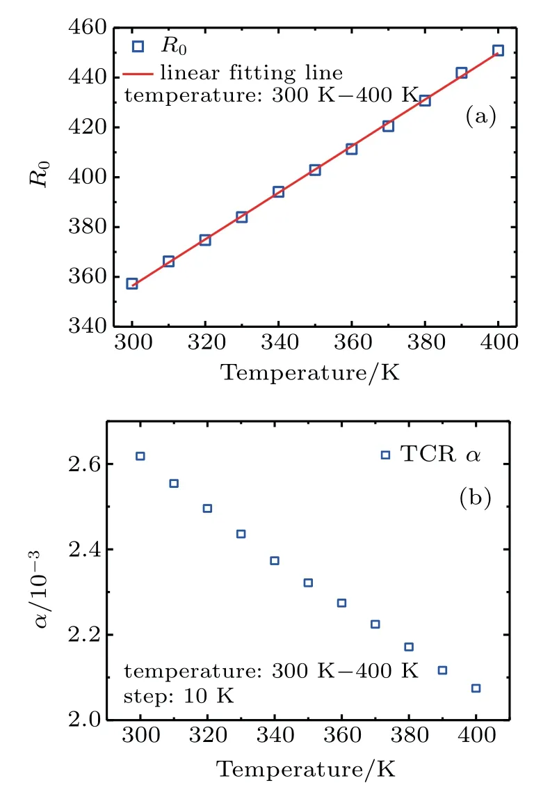
Fig.3. (a)The initial resistances R0 extracted from the resistance distribution varied as the pulse time increased, and R0 was calculated by averaging the resistances at the third hundred nanosecond. (b)The temperature coefficient distribution at different environment temperatures ranging from 300 K to 400 K in steps of 10 K.
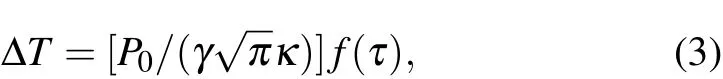
The temperature rise ΔT can be calculated using the following equation:

According to the THS model, the temperature in the metal strip can also be characterized as
where P0is the heat generation power per unit length, γ is a geometrical parameter, h is the length of the heater, κ is the thermal conductivity,and t is the measurement time.[17]The γ parameter is related to the sample structure[18]and the optical values of γ with different structures are shown in Fig.4. Here,it was set as 2 for the same structure in Fig.4(c).

Fig.4.Geometrical parameter γ is related to the measurement structure,and(a)γ =4,(b)γ =2,(c)γ =2,(d)γ =1 for the structures shown.
The thermal impedance Rthis defined as ΔT/P0, and therefore Rthcan be expressed as

When the width of the strip d is small, f(τ)is approximately proportional to lnt as given by

where D is the thermal diffusivity of the film,and τ is the characteristic time. Therefore, the thermal conductivity is related to the slope of Rthversus t in the log scale,and is given by

Figures 5(a) and 5(b) show the Rthdistributions of the control sample and of the sample with TSOI=30 nm in the same temperature region, respectively. Comparing the slope from different SOI thicknesses with that from the control sample in the same linear region, the thermal conductivity of different thin silicon films can be obtained.
As shown in Fig. 5(c), the film thermal conductivity κSi,filmcan be calculated as
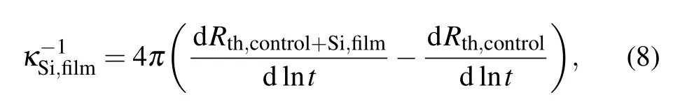

Fig.5. The linear region in thermal resistance distribution versus pulse time in log scale. The thermal resistance increased as temperature increased. (a)The control sample without SOI,(b)the sample with SOI thickness of 30 nm,and(c)the schematic of κSi,film extraction.
3. Results and discussion
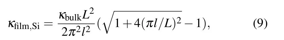
The extracted thermal conductivities of the silicon films with different thicknesses are shown in Fig.6(a). Black symbols represent the thermal conductivity of 30 nm SOI, red symbols are the thermal conductivity of 17 nm SOI, and the blue symbols are for 10 nm SOI.As the temperature increases,the conductivity does not decrease significantly, which is a similar trend to that in in-plane data.[19]This implies that internal scattering is not dominant in the present temperature regime since the Umklapp scattering has 1/T dependence on temperature.[20]The ratio of the thermal conductivity of 30 nm, 17 nm, and 10 nm SOI over the bulk value is only~6.9%,~4.3%,and ~3.8%at 300 K,respectively. This extremely low thermal dissipation in devices or circuits may result in hot spots,which interrupts smooth operation. Also,we measured the temperature response of films of the above three thicknesses in the low temperature region (75-285 K). The data are shown in Fig. 6(b). The values at a cryogenic temperature from 75 K to 210 K gradually increase as temperature rises.Beyond 210 K,the thermal conductivity goes up to a certain level. The positive temperature dependence indicates that the phonon-boundary scattering dominates in ultra-thin silicon films below 210 K.
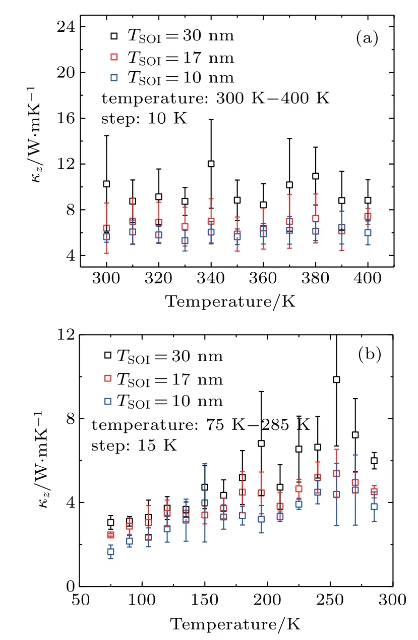
Fig.6. The cross-plane thermal conductivity extracted at temperatures(a)from 300 K to 400 K,and(b)from 75 K to 285 K.
According to the work reported in Ref.[21],the average mean free path(MFP)in nanostructured silicon films is about 200 nm. As the film thickness in this work is much smaller than the MFP, phonons can carry heat without internal scattering. In Ref.[12], a ballistic heat transport model based on extended irreversible thermodynamics was used to calculate the cross-plane thermal conductivity. The EIT model was first proposed by Alvarez and Jou,and was very effective for predicting cross-plane thermal conductivity in silicon films.[10]The analysis form is given by
where κfilm,Siis the cross-plane thermal conductivity, κbulkrefers to the silicon bulk thermal conductivity, L is the thickness of the thin film,and l is the phonon mean free path.When L is smaller than l,phonons can transport heat without internal scattering,and the above formalism can be simplified as

Comparison of the calculated results from the EIT model and the experiment data is shown in Fig. 7(a). The bulk silicon thermal conductivity κbulkand the average mean free path l are cited from the references.[9,22]It can be found that a satisfactory match between the calculated and experimental results is achieved.This indicates that the ballistic phonon transport dominates in vertical heat conduction in ultra-thin silicon films below 50 nm. The underestimate of TSOI=30 nm in the low temperature region may be attributed to the poor interface quality between Al2O3and SOI films,which could result in a large interface thermal resistance increase as the temperature decreases. The extracted thermal conductivities also match well with the data simulated using the Landauer method as show in Fig.7(b).[23]The consistency between the experiment data and the simulation values validates the feasibility of the ultrafast THS method for cross-plane thermal conductivity extraction.

Fig.7. The comparison of experimental data with the values calculated from(a)the EIT model from the low temperature region 75 K to high temperature 400 K,(b)the Landauer method in Ref.[23].
4. Conclusion
The sub-20 µs ultra-fast THS method has been implemented for measuring the cross-plane thermal conductivity of ultra-thin silicon films. The cross-plane thermal conductivities of 30 nm, 17 nm, and 10 nm thin silicon films were successfully extracted for the first time. The ratio of the thin film’s thermal conductivity over the bulk value is only about 6.9%,4.3%,and 3.8%at 300 K,respectively. The experimental data show a satisfactory agreement with the EIT model and the Landauer model, indicating ballistic phonon transport in the vertical temperature gradient direction of the silicon films.The measured thermal conductivities of silicon films provide important guidance in dealing with the self-heating related issues in advanced transistors.The results in this study also suggest possible thermoelectric applications for ultra-thin silicon films.
杂志排行

Chinese Physics B的其它文章
- Topological magnon insulator with Dzyaloshinskii-Moriya interaction under the irradiation of light∗
- Wavelength dependence of intrinsic detection efficiency of NbN superconducting nanowire single-photon detector∗
- Artificial solid electrolyte interphase based on polyacrylonitrile for homogenous and dendrite-free deposition of lithium metal∗
- Effects of CeO2 and nano-ZrO2 agents on the crystallization behavior and mechanism of CaO-Al2O3-MgO-SiO2-based glass ceramics∗
- Modulation of magnetic and electrical properties of bilayer graphene quantum dots using rotational stacking faults∗
- Thickness-dependent magnetic anisotropy in obliquely deposited Fe(001)/Pd thin film bilayers probed by VNA-FMR∗