Topological superconductivity in a Bi2Te3/NbSe2heterostructure:A review∗
2019-06-18HaoZheng郑浩andJinFengJia贾金锋
Hao Zheng(郑浩)and Jin-Feng Jia(贾金锋)
School of Physics and Astronomy,Shanghai Jiao Tong University,Shanghai 200240,China
Keywords:topological insulator,topological superconductor,Majorana zero mode,scanning tunneling microscopy,molecular beam epitaxy
1.Topological superconductor theory
Recent decades have seen a flurry of research on topological matter,including topological insulators,topological semimetals,and topological superconductors.[1-74]Nontrivial topology in solid state systems refers to a non-zero Berry phase carried by the occupied states of Bloch wavefunctions in an insulator or of the Bogoliubov-de-Gennes states in a superconductor,as well as the wavefunctions on the Fermi surface enclosing Dirac or Weyl nodes in a semimetal.Although topological insulators are the first experimentally discovered class of nontrivial topological materials,theoretical investigation of topological superconductors started almost twenty years ago,even before the term “topological matter”was introduced.The initial theoretical proposal,which found the first unconventional superconductor carrying a non-zero Berry phase,was the so-called chiral p-wave superconductor in two dimensions,whose order parameter possesses a form of Δeiθ= Δ(px+ipy).where Δ is the intensity of the order parameter,θ is the phase,and px,pyare the momenta in two dimensions.The minimal model of a two-dimensional chiral p-wave topological superconductor is described by the Bogoliubov-de-Gennes mean field theory and reads as follows:
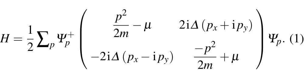
Note that this model ignores electron spin,and thereforeΨpis a spineless Nambu spinor(cp,c+-p)T.Here,p2=p2x+p2yand p2/2 m-µdepicts a single-band(free-electron like)metal in its normal state with chemical potentialµ.The Hamiltonian can be easily diagonalized and the quasiparticle eigenvalues areBased on the formulae of the eigenvalues,one can find the existence of a nodeless full superconducting gap as a feature of the two-dimensional chiral p-wave superconductor.This model intrinsically breaks time reversal symmetry,although the system does not display magnetism.In the case ofµ>0,the occupied states deduced from this model carry non-zero Berry phase in the first Brillouin zone.In other words,the model describes a superconductor with nontrivial topology.
After the discovery of this purely theoretical model described by Eq.(1),several realistic theories were proposed to realize the chiral-p wave superconducting order parameter,e.g.,the Kitaev chain and spin triplet paring.[75-85]However,these proposals still remain elusive for further experimental veri fication.
A breakthrough in realizing a topological superconductor occurred after the discovery of topological insulators.In a topological insulator,the bulk energy bands are fully gapped,while a gapless metallic surface state is guaranteed to exist by topological band theory. Furthermore,in momentum space,the surface energy band must connect two timereversal-symmetry invariant points odd number of times.In other words,there must exist odd numbers of two-dimensional(2D)surface Dirac cones with helical spin textures inside the bulk energy gap of a topological insulator.[1-3]Until now,the most ideal topological insulators discovered by experiments have been the Bi2Te3-class materials,including Bi2Se3,Bi2Te3,and Sb2Te3.[10-12]These materials possess only one helical Dirac cone on their surfaces.The surface band itself(a two-dimensional helical Dirac cone)carries a π Berry phase,whose Hamiltonian reads as Hsurf=(p×s)·ˆz,where p is the momentum of a surface electron,s is its spin andˆz is the unit vector of a surface normal.Fu and Kane found that introducing a conventional s-wave pairing to the helical Dirac surface state on a topological insulator can mimic an effective 2D chiral p-wave superconductor.[86]The Fu-Kane Hamiltonian reads as
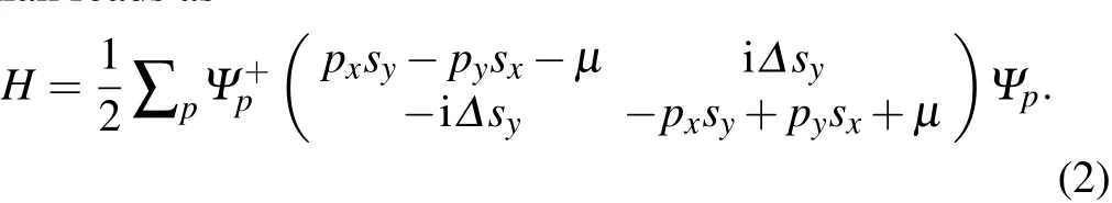
In this model,Ψpis a full Nambu spinor.The eigenvalues of this Hamiltonian arewhich is also fully gapped.By taking the off-diagonal terms in Eq.(2)as a first order perturbation and solving the Hamiltonian by assuming Δ=0 to get the eigenstates,the effective Hamiltonian of Eq.(2)under a first order perturbation approximation is nothing but a 2D spinless chiral p-wave superconductor modeled by Eq.(1).This proposal,which is based on an unconventional surface state of a superconducting topological insulator,has proved to be practical in experiments.[87-89]We will discuss the experimental results in detail later.
The most exciting phenomenon in a 2D topological superconductor is the existence of a Majorana-type excitation inside the Abrikosov magnetic vortex core states.In a type-II superconductor,the magnetic field is able to penetrate into the bulk of the superconductor in a number of discrete areas.In each area,the magnetic flux is quantized in terms of h/2e(where h is the Planck constant and e is the charge of an electron)and locally breaks the superconductivity.Such an area,whose diameter is the London penetration length and whose flux is quantized in h/2e,is called an Abrikosov magnetic vortex.Thus the Abrikosov vortex produces a superconducting/nonsuper conducting interface.Importantly,a quasi particle which moves in a circle around an Abrikosov vortex once will pick up an additional geometrical phase of π in its wave function.This generates the so-called anti-periodical condition,Ψ0(r,θ +2π)=eiπΨ0(r,θ)=-Ψ0(r,θ),where r and θ are polar coordinates in 2D.By solving Eq.(2)inside an Abrikosov vortex core with the anti-periodical boundary condition,one can obtain a bound state at zero energy with eigenstateBy projecting this state with its Nambu basis and integrating over the full space,one can get the field operator,which is
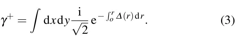
Two important consequences can be easily deduced from the zero-energy solution of Eq.(3).Firstly,the creation operator is equal to its annihilation operator,γ+=γ,which means that the anti-particle of this quasiparticle is itself.It is exactly a Majorana fermion.Therefore,the zero-energy bound state inside an Abrikosov vortex on a 2D topological superconductor is also named a Majorana-zero-mode.Secondly,the Majorana-zeromode only contains the spin up operator of an electron.This indicates that a Majorana-zero-mode is a spin polarized state which can be controlled by an external magnetic field.
Topological superconductors and Majorana-zero-modes are two important topics in contemporary condensed matter physics,materials science and nanotechnology,with many important and recently published theoretical and experimental results.[56-70,87-89]This article will review our experimental realization of an effective topological superconductor and a Majorana-zero-mode.
2.Scanning tunneling microscopy
The primary apparatus with which to experimentally verify a topological superconductor and detect a Majorana-zeromode is scanning tunneling microscopy(STM).STM is designed based on quantum tunneling:by bringing a sharp metallic tip very close(usually within 1 nm)to a clean surface of a conducting sample,electrons can tunnel through the vacuum barrier and form a current with a small potential difference(usually less than 10 V)between the tip and sample,much smaller than the value required to generate a field emission effect.Importantly,by fixing the bias voltage,the intensity of the tunneling current is exponentially proportional to the tip-sample distance.A variation of 0.1 nm in the tipsample distance will induce a change of one order of magnitude in the tunneling current.Thus the atomic corrugation of a clean surface can be detected by measuring the local value of the tunneling current.This is the principle of using STM to obtain an atomic image of a solid surface.However,the real working condition of an STM is usually not to directly detect the change in tunneling current under a constant bias voltage.Instead,it usually measures tiny changes in the tip position under a constant current by adjusting the tip-sample distance via a feedback mechanism and records the value at each measuring point to produce a 2D image.
The tunneling current at each point can be precisely calculated using the modi fied Bardeen model,which reads as follows:
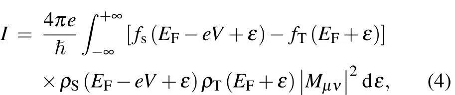
where f is the Fermi distribution function and ρ is the density of states at the energy indicated in the bracket.The subscripts S and T stand for the sample and tip respectively.Mµνis the tunneling matrix element between the wave functions of sample and tip.
By assuming that the tip density of states in an STM is constant near its Fermi level and that the tunneling matrix Mµνis not dependent on energy and is thus a constant,one can easily obtain the formula of the dI/dV intensity:
Equation(5)reveals that the dI/dV signal is directly proportional to the density of states in the sample.In STM,a lock-in amplifier is usually employed to detect the first derivative of the tunneling current by modulating the bias with a single frequency AC voltage.To obtain a reproducible dI/dV signal,a low temperature is required to minimize the thermal drift of an STM tip.Therefore nowadays STM is often mounted inside a liquid helium Dewar,sometimes with a superconducting coil installed to generate a high magnetic field.
By measuring the dI/dV spectrum at each point and sweeping over an area of the sample surface,one can obtain the so-called dI/dV map,which is a powerful and widely used method for probing many important physical phenomena,such as wave function mapping,quasi particle interference imaging and the local gating effect.[90-106]
Spin-polarized STM and STS have been successfully achieved in previous studies.[107-110]By coating an oxide-free metallic tip,usually made of W,with a thin film of magnetic materials,such as Fe or Cr,one may be able to realize a spin polarized tunneling current and thus can detect magnetic properties of a nanostructure or an atomic subject.
In our investigation of a topological superconductor and a Majorana-zero-mode,we use dI/dV spectroscopy(sometimes with spin polarized tips)and dI/dV map techniques with and without magnetic fields.
3.Topological superconductor based on Bi 222Te 333/NbSe 222heterostructure
According to Fu-Kane theory,a topological insulator is a critical building block of chiral p-wave superconductors.Bi2Se3and Bi2Te3are the most ideal topological insulators found so far due to their large bulk energy gap(about 300 meV)and the presence of only one spin-momentum locked Dirac cone on their surfaces.Therefore,most of the attempts towards realizing topological superconductors are based on Bi2Te3-class materials.There are two main methods for introducing s-wave superconductivity into the helical Dirac surface states of topological insulators,namely by chemical doping or the superconducting proximate effect.Cu-,Sr-,and Nb-doped Bi2Se3samples have demonstrated superconductivity.[111-114]Although a number of interesting effects have been detected on these superconducting doped topological insulators,for example,zero energy states and electronic nematicity,[115]evidence of Majorana-zero-modes inside the Abrikosov vortex core is still controversial.[116]The second approach,which is based on the superconducting proximate effect,has been proved to be the only practical way.
The superconducting proximate effect means that by attaching a thin layer of normal metal to a superconductor,the superconductor order parameter can penetrate into the normal metal at the length scale of the superconductor’s coherent length,and thus drive the normal metal into a superconducting state.The intensity of the superconductivity,i.e.,the size of the superconducting gap,will decay with the distance away from the normal metal/superconductor interface.Obviously,a thin film of normal metal with a thickness much less than the coherent length of the superconductor is desirable to achieve a superconducting proximate effect.This is the motivation to prepare an atomically thin film of Bi2Te3.[117-121]
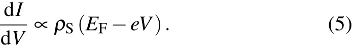
As shown in Fig.1(a),Bi2Te3is a layered material.The five Bi-Te-Bi-Te-Bi atomic layers form a basic unit cell,also named a quintuple-layer(QL),with strong covalent bonding between the atoms.The inter-QL interaction is the weak Van der Waals forces,which allow the Bi2Te3sample to be easily cleaved between QLs,leaving the Te atomic plane as the surface termination.We employed molecular beam epitaxy(MBE)to grow the Bi2Te3thin films.MBE is an elaborate apparatus for preparing very high-quality single-crystal thin films,which has the capability to control the thickness of the thin film down to only one atomic layer.In the MBE growth of Bi2Te3we evaporated high purity Bi and Te raw materials simultaneously by individual Knudsen effusion cells and condensed the material on a substrate,Si or 2H-NbSe2.By precisely controlling the temperatures of source and substrate,we can achieve single-crystalline thin film of Bi2Te3with an atomically flat surface,displayed in the STM image in Fig.1(b).Layer-by-layer growth of thin films,where after finishing a complete layer of a material the additional layer starts to form,enables one to prepare an ultra-thin- film while controlling the exact number of atomic layers.High-energy re flection electron diffraction is widely used in MBE systems to monitor the growth process in real time.The oscillation of the intensity of the diffraction spot is the “smoking gun”evidence of layer-by-layer growth.Figure 1(c)demonstrates such oscillation curves in our experiments,which prove that the layer-by-layer mode is achieved in our Bi2Te3growth on a Si substrate with a growth rate of one QL per approximately 5 min.
Topological insulators carry nontrivial topology in their bulk,where the topological invariant is the Z2index.The Z2nature of the topology results in the effect that if the film is too thin,the surface states on the top and bottom surfaces in the thin film topological insulator can hybridize,which will gap out the Dirac node.Therefore, finding the thickness limit above which the topological insulator surface state can survive is a valuable task.We employed MBE to prepare a series of Bi2Te3thin films with increasing thicknesses and used angle resolved photo emission spectroscopy(ARPES)to exam the surface energy band structures.[118]Figures 1(d),1(e),and 1(f)present the ARPES maps which measure the surface bands along theΓ-M direction on Bi2Te3thin films with thicknesses of 1 QL,3 QL,and 5 QL,respectively.On the 1-QL Bi2Te3surface,ARPESclearly observes a free-electron-like parabolic dispersed surface state and a broad bulk valence band at about 500 meV below the Fermi level.There is an approximately 300 meV energy gap between the bottom of the surface state and the top of the bulk valence band.The lack of evidence to show a Dirac-cone shaped surface band proves heavy hybridization between the top and bottom surfaces on this 1-QL thin film.The situation drastically changes if we increase the Bi2Te3film to 3 QLs.As shown in Fig.1(e),an electron pocket from the bulk conduction band appears at the Fermi level and a hole pocket from the bulk valence band is located below-380 meV.In between,a linearly dispersed surface band is explicitly resolved,and is the evidence of the formation of the Dirac-cone-type topological surface state.Further increasing the Bi2Te3film thickness to 5 QLs,the topological feature in the Bi2Te3energy bands remains intact.Therefore,the thick ness limit of aBi2Te3thin filmon Sisubstrateis 3QL.
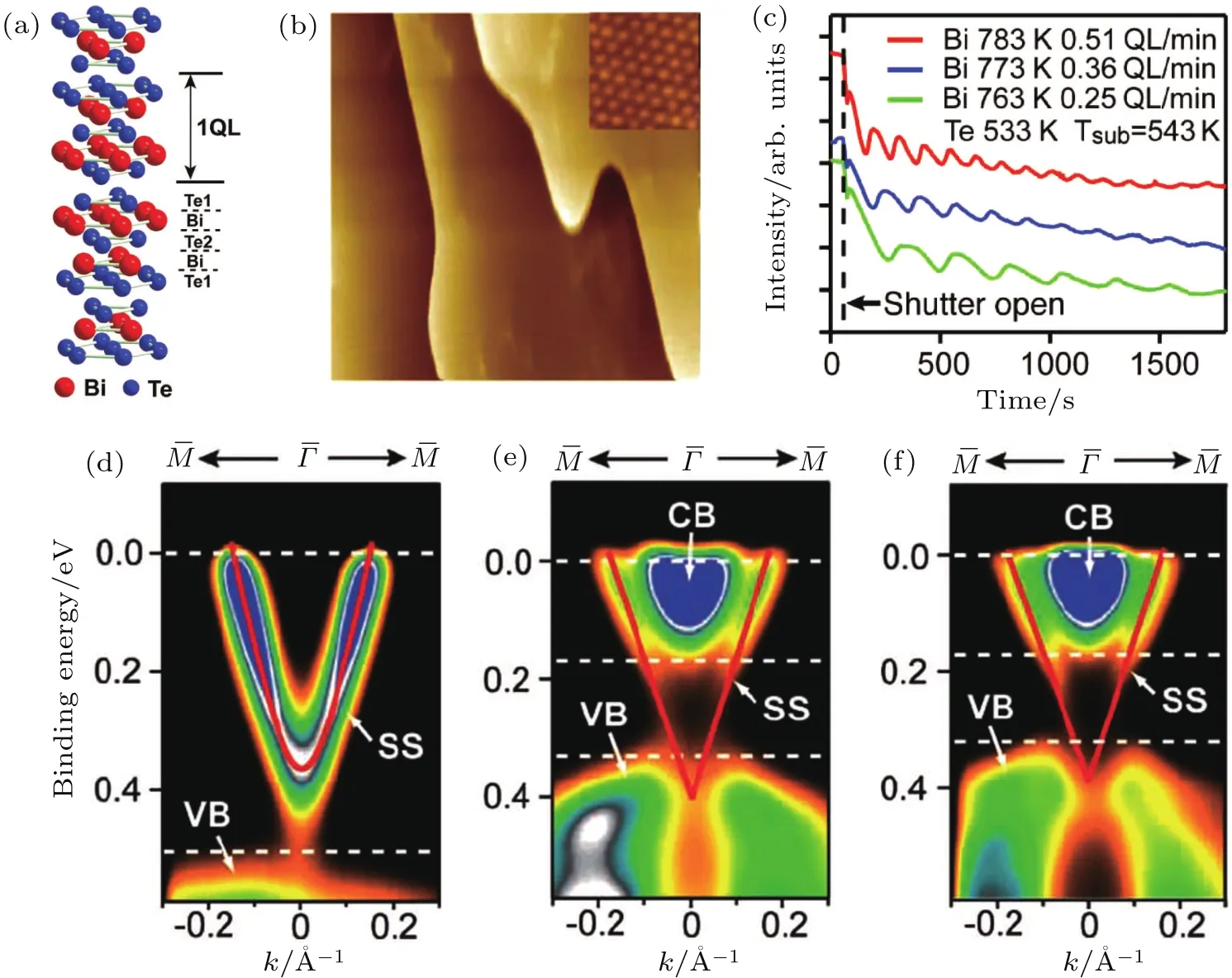
Fig.1.(a)astruc turemodel of the Bi2Te3topologi calinsulator,(b)ascanning tunneling microscope(STM)image(500nm×500nm)demonstrating the atomically flat epitaxial Bi2Te3thin film.Inside is the Bi2Te3lattice(2.5 nm×2.5 nm),(c)high-energy re flection electron diffraction intensity oscillation curves proving the layer-by-layer growth mode of Bi2Te3thin films under the indicated parameters.The remaining figures show angle resolved photoemission spectroscopy(ARPES)intensity maps from Bi2Te3thin films of 1(d),3(e),and 5(f)quintuple-layers at liquid nitrogen temperature.All panels are adopted from Ref.[118].
After ascertaining the growth condition of Bi2Te3on the Si substrate,we moved to prepare the thin film topological insulator on a superconductor.2H-NbSe2is a layered material with a superconducting transition temperature at 7 K and with a conventional s-wave paring symmetry.Instead of Bi2Te3,we choose its cousin material Bi2Se3to grow on NbSe2because both the epitaxial layer and the substrate are selenides.Figures 2(a)-2(c)demonstrate the ARPES band maps at 3 QL,6 QL,and 9 QL of Bi2Se3thin films with NbSe2substrates,respectively.[70]For the 3-QL sample,the data reveal an electron pocket with Rashba-type spin-orbital band splitting from the bulk conduction band of Bi2Se3and a weak hole pocket from the bulk valence band of Bi2Se3.Inside the bulk energy gap,a free-electron-like parabolic shaped band rather than a Dirac-cone shaped surface band can be discerned.This proves that 3 QL is too thin to establish the topological properties of a Bi2Se3thin films on NbSe2.For the sample with 6-QL thickness,one can observe a number of parabolic electronic bands at the Fermi level,these are the quantum well states of the bulk conduction band of Bi2Se3due to the finite size confinement in the surface normal direction.Between the conduction and valence bands,a Dirac-cone shaped surface state is clearly resolved.The Dirac node is located at the binding energy of about 420 meV,which is distinguishable from the bulk valence bands.The ARPES measurement of the 9-QL sample gives rise to an almost identical result when compared to the 6-QL sample.This thus proves that 6 QL is the thickness limit of a Bi2Se3film on NbSe2substrate.
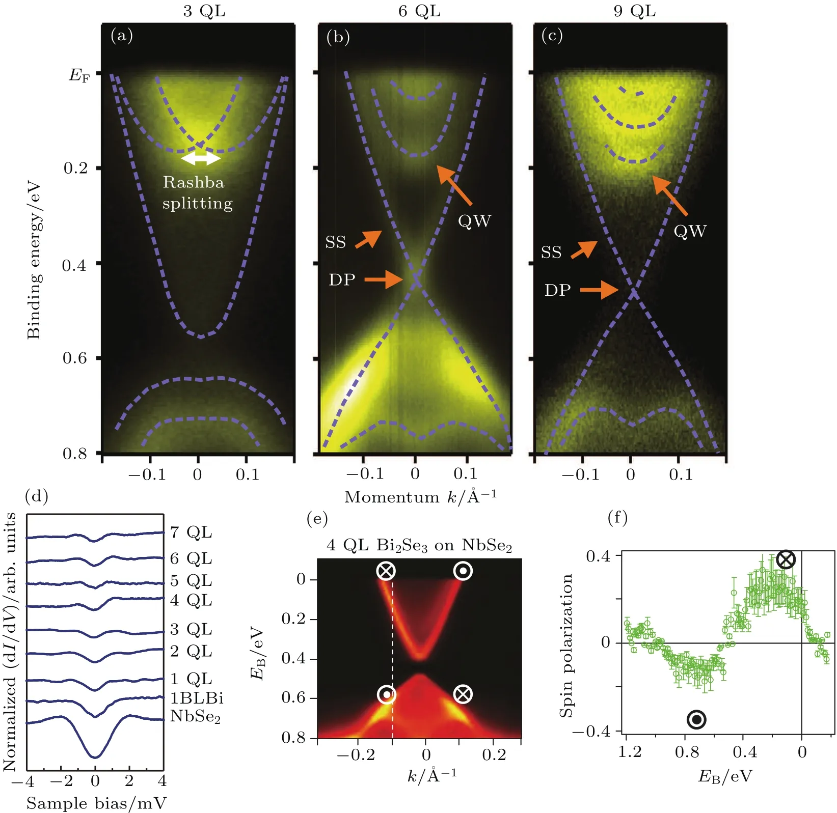
Fig.2.ARPES intensity maps of 3(a),6(b),and 9(c)QL of Bi2Se3thin films grown on 2H-NbSe2superconductors.(d)dI/dV spectra demonstrating that the superconducting gap on the Bi2Se3thin films is at the indicated thickness.(e)and(f)Spin-resolved ARPES data for a 4-QL Bi2Se3thin film on a NbSe2substrate.Panels(a)-(d)are reproduced from Ref.[70],while panels(e)and(f)are from Ref.[120].
The two key factors to realize a Fu-Kane-type topological superconductor are the coexistence of an s-wave superconductor order parameter and the spin helical Dirac-type surface state.Our dI/dV spectra of bare NbSe2and Bi2Se3films with different thicknesses at a sample temperature of 4.2 K are displayed in Fig.2(d).[70]The spectra on Bi2Se3thin films up to 7 QL also demonstrate superconducting gaps at the Fermi level.In addition to the fact that NbSe2features an s-wave superconducting gap in the dI/dV spectrum(not shown here),we con firm that the epitaxial Bi2Se3thin films become superconducting with s-wave paring through the proximate effect.The next important issue is the evidence of helical spintextured Dirac surface states on the samples.Xu et al.reported their spin-resolved ARPES results,which are presented in Figs.2(e)and 2(f).They measured the surface states of 4-QL Bi2Se3thin films on a NbSe2substrate.By identifying the spin orientation of these electrons on the surface bands at the Fermi level,they discovered that the spins were locked to the electron momenta,and that the spin con figurations were opposite to each other,by comparing the electrons from the left and right propagating branches of a surface Dirac cone.In other words,the helical spin textures establish on the 4-QL Bi2Se3thin film.Taking the aforementioned experimental evidence together,we now know that Fu-Kane-type topological superconductivity is realized on Bi2Se3epitaxial thin films with thicknesses larger than 4 QL,which are deposited on a conventional s-wave superconductor 2H-NbSe2.
4.Majorana zero mode
Our experimental detection of a Majorana-zero-mode is based on the Bi2Te3thin films on the NbSe2substrate.Due to almost identical physical properties,especially the analogous bulk and surface band structure between Bi2Te3and Bi2Se3,we believe that the Bi2Te3/2H-NbSe2heterostructure is also an effective chiral p-wave topological superconductor.Indeed,our experiment veri fies this point.[121-123]
In order to experimentally detect a Majorana-zero-mode,the location of the Fermi level is critical.Previous theoretical work has established that if only the Fermi level cuts through the surface energy bands, the Majorana-zero-mode will be easily and clearly resolved.However,if the bulk bands of the topological insulator films also contribute to the low energy excitations,the Majorana-zero-mode will carry a discrete angular momentum and become more complicated.The paradoxical issues escalate if the Fermi level only passes surface states.This situation means that the bulk of the thin film topological insulator is insulating,which will extensively suppress the superconducting proximate effect.Therefore,one has to search for an optimized sample to realize a Majorana-zeromode.Shown in Fig.3(a),we measured large-energy-scale dI/dV spectra of 3-QL and 5-QL Bi2Te3epitaxial films on a NbSe2substrate.Both spectra show typical insulator behavior with well-de fined energy gaps.The red and blue arrows point to the bulk conduction and valence bands respectively.It can be seen that on the 3-QL sample,the bulk conduction-band bottom is located at about 100 meV below Fermi level,which means that a large part of bulk state exists at the Fermi level.On the contrary,the bulk conduction-band bottom of the 5-QL sample sits almost exactly on the Fermi level,which renders the sample an ideal platform for detecting a Majorana-zeromode.Moreover,we also measure small-energy-scale dI/dV spectra on a series of hetero structures with different Bi2Te3film thicknesses at the sample temperature of 0.4 K.On all Bi2Te3films with thicknesses from 1 QL to 11 QL,superconducting gaps can be clearly discerned.[121]
Another important issue in realizing a Majorana-zeromode is the confirmation of the existence of an Abrikosov vortex.It requires both the superconducting substrate and the superconducting thin film topological insulator induced by the proximate effect to be type-II superconductors.The reason we choose NbSe2as a substrate is not only because it is a layered material which can be easily cleaved,but also because it is a type-II superconductor.Indeed,our zero energy dI/dV map taken on bare NbSe2under a magnetic field of 0.75 T reveals a hexagonal symmetric Abrikosov vortex lattice.Furthermore,on our 3-QL Bi2Te3/NbSe2heterostructure,an Abrikosov vortex lattice with slight disorders can be resolved,this is displayed in Fig.3(c).To summarize,our Bi2Te3/NbSe2heterostructure is ready to test a Majorana-zeromode in its Abrikosov vortex core state.[121]
4.1.The spatial properties of a Majorana-zero-mode
A Majorana-zero-mode is located at zero energy and is expected to give rise to a zero-bias peak in a small-energyscale dI/dV spectrum.It is thus speculated to discover an Majorana-zero-mode merely by observing a zero-bias peak in a dI/dV spectrum.However,this simple proposal is not correct since one can also obtain a zero-bias peak in the Abrikosov vortex core on NS,which is clearly not a topological superconductor.In a real material system,the conventional in-gap states,so-called Caroli-de Gennes-Matricon states,must be taken into account.Inside an Abrikosov vortex,the magnetic field can destroy the superconductivity in the vortex’s central area and thus drive the vortex core to a normal metal state.Previous theoretical work found that normal metal states at the vortex core could also become quantized,with the several excited states inside the superconducting gap.In a topological insulator/s-wave superconductor heterostructure case,the first excited Caroli-de Gennes-Matricon state is located at the energy ofwhere Δ is the superconducting gap on the topological insulator surface and E is the energy distance from the Fermi level to the energy of the surface Dirac node.[124-131]In our experiment,due to a Δ of only about 1 meV and an E of about 100 meV,the first excited state in the Bi2Te3/NbSe2heterostructure is at only about 0.01 meV.This Caroli-de Gennes-Matricon state is so close to zero energy that it is already beyond the energy resolution of any model experiments,and thus manifests itself as a zerobias peak in a dI/dV spectrum.Therefore,solely detecting a zero bias peak is far from “smoking gun”evidence to prove the exitance of an Majorana-zero-mode.
We designed a method to ambiguously verify the Majorana-zero-mode based on its spatial properties.Previous theoretical work[87]found that the spatial distribution of a Majorana zero mode could be described by
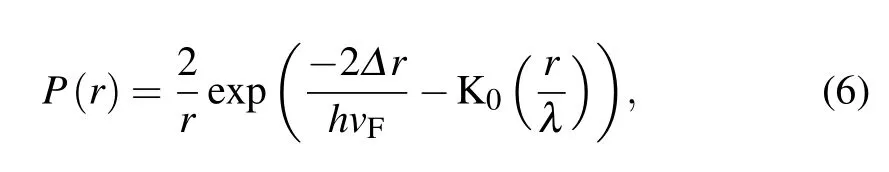
where P(r)describes the occupation possibility of a zero mode at a distance r away from the center of an Abrikosov vortex.Δ is the superconducting gap of the topological insulator surface states.vFis the Fermi velocity of the Bi2Te3thin film’s surface band.λ is the London penetration length.K0is a zero-order modi fied Bessel function.Equation(6)reveals that the occupation possibility of a Majorana-zero-mode,i.e.,the spectral weight of a zero-bias peak in a dI/dV spectrum,slowly decays with distance r instead of abruptly dropping to zero.It indicates that the existence of a Majorana-zero-mode gives rise to a spatial range of dI/dV spectrum peaks exactly located at zero energy.On the contrary,a Caroli-de Gennes-Matricon state cannot persist with its energy when moving away from the Abrikosov vortex center.Instead,this state will shift to a higher energy as r changes.The different spatial distribution between a Majorana-zero-mode state and a Caroli-de Gennes-Matricon state is used to distinguish a Majorana-zeromode.
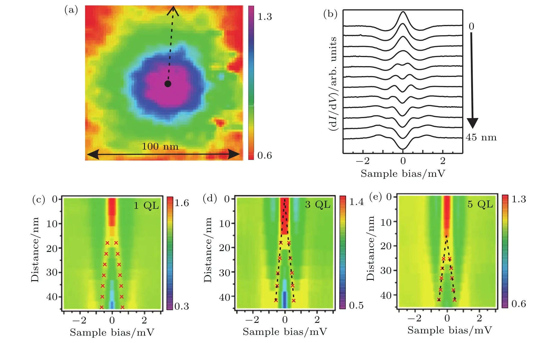
Fig.4.(a)A single Abrikosov vortex map,(b)a series of dI/dV spectra measured along the dotted line in panel(a).(c)-(e)False color plots of the spectra.The data were measured for a 1-QL Bi2Te3/NbSe2sample,showing an inverse V-like shape splitting of the zero bias peak.However,in both the 3-QL and 5-QL samples,inverse Y-shaped splitting behaviors are observed,which indicates the existent of a Majorana zero mode.All panels are reproduced from Ref.[122].
In order to find a Majorana-zero-mode,a single Abrikosov vortex was adopted rather than Abrikosov vortex lattice,because the vortex interaction inside a vortex lattice could destroy a Majorana-zero-mode.In our Bi2Te3/NbSe2heterostructure,we found that the Majorana-zero-mode survived at a magnetic field below 0.18 T.Figure 4(a)displays a single Abrikosov vortex map.We measured a series of position-dependent dI/dV spectra to exhibit the spatial evolution of the in-gap states.[122]
In Figs.4(c)-4(e),we plot the position-dependent dI/dV spectra as false-color coded three-dimensional maps,where the x axis shows bias voltage,the y axis represents the distance away from an Abrikosov vortex center,and the color code stands for the intensity of the dI/dV signal.For both 1 QL and 3 QL of BT films on NS,it can be seen that the zero bias peaks immediately split into two peaks whose energies are not at zero any more,when moving away from the Abrikosov vortex center.However,for the 5-QL sample,the situation is clearly different.The dI/dV peak remains at zero bias even at a distance of 20 nm away from the Abrikosov vortex center.Based on the comparison,we conclude that an Majorana-zero-mode with a spatial size of 20 nm was explicitly detected in a single Abrikosov vortex on our 5-QL Bi2Te3/NbSe2heterostructure.
4.2.The spin properties of a Majorana-zero-mode
Based on Fu-Kane theory,i.e.,Eq.(3),a Majorana-zeromode arising from an s-wave superconducting topological insulator surface state is fully spin polarized.Later,a more complicated theory considered not only the surface state but also the bulk state in a topological insulator and discovered that a Majorana-zero-mode possesses a quantized total angular momentum j,where j=l+s/2-1/2.l and s are the orbit and spin angular momentums respectively.[127,128]It was revealed that the topological bound states in an Abrikosov vortex core(anti clockwise wound)read as
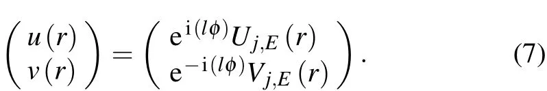
Uj,E(r)and Vj,E(r)are the electron and hole wavefunctions,respectively.r and φ are the length and angle of a two dimensional(2D)vector,respectively.If the total angular momentum is j=0 and energy is E=0,the state can be recognized as a Majorana-zero-mode.Moreover,the Majoranazero-mode is predicted to be doubly degenerate.j=0 requires either l=0 and s=1(a spin up state)or l=1 and s=-1(a spin down state).More importantly,the theory revealsthat the spectral weight of a spin up Majorana-zero-mode is much stronger than that of a spin down state in the center of an Abrikosov vortex.In other words,even when the influence from the topological insulator’s bulk band is considered,the Majorana-zero-mode in the vortex center can still be treated as a spin polarized state.To date,there have been no other low energy bound states which are spin polarized.Therefore,this spin property is unique to a Majorana-zero-mode.
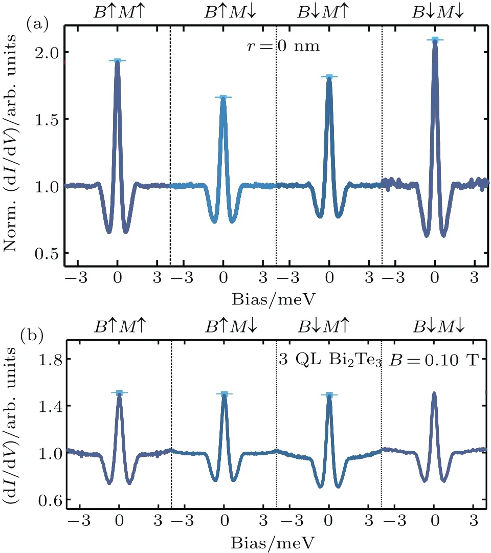
Fig.5.(a)Polarization-dependent dI/dV spectra measured at the geometric center of a vortex under a magnetic field of 0.1 T and temperature of 40 mK on a 5-QL Bi2Te3/NbSe2sample.B controls the spin direction of a Majorana zero mode,while M is the spin-polarization direction of the tip.When the polarizations are parallel between the tip and the Majorana zero mode,the intensity of the zero-bias peak is enhanced,and when the polarizations are antiparallel,the intensity is suppressed.Panels(b)shows similar spectra to panel(a)but measured on a 3-QL Bi2Te3/NbSe2sample.No polarizationde pendent zero-bias peak intensity of dI/dV contrast can be observed.All panels are reproduced from Ref.[123].
In an STM measurement,if one replaces the tip from a normal metal to a magnetic metal,a spin polarized STM is achieved.In our ultra-low temperature(30 mK)STM experiments,we coated clean W wire with several tens of nm of Fe.The Fe tip can be polarized by external magnetic field at about 2 T and remain polarized at a field below 2 T.On the contrary,a field of only about 0.1 T is required to create a Majorana-zero-mode in a single Abrikosov vortex core state on our Bi2Te3/NbSe2samples.[123]In Fig.5(a),we show a series of polarization dependent dI/dV spectra measurements on the center of an Abrikosov vortex at 0.1 T on our 5-QL Bi2Te3/NbSe2heterostructure.These data show that if the polarizations of the tip and the Majorana-zero-mode are in the same direction,the dI/dV signal is enhanced.If the polarizations are antiparallel to each other,the dI/dV signal is suppressed.This phenomenon is induced by the spin dependent Andreev re flection which comes from a Majorana-zeromode.In controllable experiments,no obvious polarizationdependent variations in dI/dV zero bias peak intensity can be observed in the 3-QL(and thinner)Bi2Te3/NbSe2samples,because no Majorana zero modes exist on these samples.We thus experimentally established the spin-polarized nature of a Majorana-zero-mode in the Abrikosov vortex center.
5.Summary
In this article,we brie fly review our recent experimental progress in realizing an effective chiral p-wave topological superconductor in Bi2Te3/NbSe2heterostructures with a Bi2Te3thin filmthickness higher than 4QL,all preparedby molecular beam epitaxy.Under a magnetic field below 0.18 T,we discovered a Majorana-zero-mode existing inside an Abrikosov vortex core state.The Majorana-zero-mode occurs in an area with radius of about 20 nm.Moreover,the Majorana-zeromode at the position of the vortex center carries a spin polarized con figuration.Our results open a new avenue toward non-Abelian statistics and future’s fault tolerance quantum computation.[56-62]
杂志排行

Chinese Physics B的其它文章
- The universal characteristic water content of aqueous solutions∗
- Neutral excitation and bulk gap of fractional quantum Hall liquids in disk geometry∗
- Direct deposition of graphene nanowalls on ceramic powders for the fabrication of a ceramic matrix composite∗
- Hard carbons derived from pine nut shells as anode materials for Na-ion batteries∗
- Crystal structures and sign reversal Hall resistivities in iron-based superconductors Lix(C3H10N2)0.32FeSe(0.15<x<0.4)∗
- Improved electrochemical performance of Li(Ni0.6Co0.2Mn0.2)O2 at high charging cut-off voltage with Li1.4Al0.4Ti1.6(PO4)3 surface coating∗