Impurity-free Vacancy Diffusion Induces Intermixing in GaInP/AlGaInP Quantum Wells Using GaAs Encapsulation
2018-08-28TIANWeinanXIONGCongWANGXinLIUSupingMAXiaoyu
TIAN Wei-nan,XIONG Cong ,WANG Xin,LIU Su-ping,MA Xiao-yu
(1.National Engineering Research Center for Optoelectronic Device,Institute of Semiconductors,Chinese Academy of Sciences,Beijing 100083,China;2.College of Materials Sciences and Opto-Electronic Technology,University of Chinese Academy of Sciences,Beijing 100049,China)
*Corresponding Author,E-mail:xiongcong@semi.ac.cn
Abstract:Impurity-free vacancy diffusion(IFVD)induced quantum well intermixing(QWI)of red light diode laser wafer using GaAs encapsulation is explored.The wafer has an active region of a 9 nm-thick GaInP quantum well and two 350 nm-thick AlGaInP barriers.The GaAs dielectric layer is prepared through MOCVD.The QWI is induced by rapid thermal annealing at 950℃ at different times and different thicknesses of GaAs.Blue shifts and full width at half maximum(FWHM)are obtained through photoluminescence tests.A maximum blue shift of 53.4 nm is obtained at 120 s and an optimal FWHM of 18 nm by the IFVD-induced QWI is noted at 1 min.
Key words:blue shift;impurity-free vacancy diffusion;quantum well intermixing;diffusion
1 Introduction
There is a continuous demand for ever higher power and efficiency from semiconductor lasers.State-of-the-art high power lasers require not only sophisticated design but also complex fabrication technologies to push the boundaries.A major obstacle to higher power is catastrophic optical mirror damage(COMD)that occurs at the mirrors of the cavity[1].Even when the near mirror regions are not electrically pumped,effectively dividing the optical cavity into passive and active regions,mirror damage takes place due to light absorption by interface states between the cleaved facet and coated multilayer dielectric mirror that leads to non-radiative recombination causing the generation of heat.This large quantity of heat in a small facet surface can lead to local reduction of the band gap and COMD[2].Reduction of the band gap causes further light absorption where a positive feedback develops accelerating COMD and suddenly exceeding the damage threshold[3].
Among several approaches to improve facet stability and increase the threshold for damage,two classical approaches are taken:increase the facet surface area to reduce the power density incident on the mirrors and manipulate the local band gap near the mirrors to reduce re-absorption of light generating non-radiative recombination[4].One approach to modify the band gap at the cavity edges is to use etch-back and epitaxial regrowth or overgrowth of the wider band gap material for the quantum well.This leads to a higher facet damage threshold and the output power and electro-optical conversion efficiency are limited around 15 W and 60%,respectively[5-6].However,etch-back and regrowth at the passive waveguide sections of a laser cavity are both tedious and expensive.It further has a coupling efficiency problem at the interface between the active and passive sections of the waveguide.On the other hand,control of the band gap near the facets can also be achieved by impurity induced disordering(IID),impurity free vacancy disordering(IFVD),and laser-induced disordering(LID)[7].The IID technique is effective,but leads to free carrier absorption due to the introduction of unwanted carriers.The structure of modern lasers employing quantum wells,to generate light,surrounded by large band gap and low index waveguides and claddings gives the opportunity to intermix the quantum well using IFVD,changing its compositional profile and increasing the effective band gap close to cavity edges during fabrication.In this approach,the creation of a non-absorbing mirror(NAM)where the facet is almost transparent leads to high COMD thresholds for higher power extraction and a longer lifetime.Due to these advantages,IFVD quantum well intermixing(QWI)is preferred due to lower loss and higher optical coupling efficiency when compared with IID and selective epitaxial growth techniques[8].
The IFVD technique involves the deposition of a dielectric(impurity free),such as silicon dioxide(SiO2),on the sample surface.In this technique,defects with a lower density than that obtained using the IID technique are created.After the deposition of the dielectric,group-Ⅲ atoms,i.e.,Al and Ga,inter-diffusion between the QW and the barrier interfaces occurs,thereby blueshifting the bandgap of the material without introducing severe damage to the QWs[9-10].Because this process is essentially impurity free,the degradation of the optical and electrical properties is minimized.Beernink et al.were first to apply this technique on the InGaP/InAlGaP material system using plasma-enhanced chemical vapor deposition(PECVD)to deposit a SiO2capping layer and reported a negligible bandgap blue-shift[11].Another group annealed bare(uncapped)and SiO2-capped samples of InGaP/InAlGaP QWs at 900℃for 4 h and showed only a slight bandgap blue-shift of 10 nm[12].Kowalski et al.reported a differential shift of 100 meV using 200-nm sputter-deposited SiO2,whereas no wavelength shift was observed for devices capped with PECVD-deposited SiO2.Hamilton et al.,from the same group,reported an intermixed InGaP/InAlGaP laser emitting at approximately 670 nm.The device intermixed with this method was blueshifted(29 nm,91 meV)and demonstrated lasing at 640 nm[13].
In this paper,GaAs cover sheet was firstly introduced in the IFVD quantum well intermixing.
2 Experiments
The laser structure in this work was grown on Si-doped(100)GaAs substrate with a misorientation of 10°towards(111)A by low pressure MOVPE.Epitaxial growth was carried out in an AIX200 system which contains a horizontal reactor.During the epitaxy,the growth temperature was controlled at 650-725℃and the growth pressure was about 5 000 Pa.The source materials were trimethylaluminium(TMAl),arsine(AsH3)and phosphine(PH3).The p-type dopant was silane(SiH4).The carrier gas was palladium-diffused hydrogen.All layers include the following sequence from the substrates:a Si-doped 200-nm-thick n-GaInP buffer layer, a Si-doped 1 000-nm-thick n-Al0.7GaInP cladding layer(dopant concentration n=(5-8)×1017cm-3),a compressively strained single-quantum-well(SQW)structure(barrier:AlGaInP:350 nm,well:GaInP:9 nm),a Zn-doped 1 000-nmthick AlGaInP cladding layer(dopant concentration p=(1-2) ×1018cm-3),and a higher p-doped contact layers(dopant concentration p=(1-2)×1020cm-3),including a 50-nm-thick GaInP layer and a 100-nm-thick GaAs layer.A schematic diagram of the layers'structure is given in Tab.1.The laser was designed to have a peak emission at 660 nm.Fig.1 shows the photoluminescence(PL)spectrum at RT.
Firstly one sample was prepared for annealing without any treatment.Annealing was carried out in a rapid thermal annealing furnace(RTA).

Tab.1 Sample layer structure

Fig.1 PL spectra of the as-grown sample
The anneals were performed in the flowing N2.The room-temperature photoluminescence(PL)spectra for an untreated sample which was annealed at 950℃ for 1 min.Then we remove the GaAs layer using the etchant V(H2SO4)∶V(H2O2)∶V(H2O)=4∶1∶1),and repeated the annealing process at 950℃ for 60 s.To explore the relationship between the degree of blue shift and the thickness of GaAs,We grow the GaAs layer of 1 μm and 2 μm by MOCVD and annealed for 45 s,Then we chose the best thickness for different times of annealing.The samples were divided into four parts,all annealed at 950℃.The only difference is the annealing time.They were annealed for 60,90,120,120 s.Finally we measured their PL spectra.All the samples were annealed with as-grown samples to explore the effect of annealing conditions on the quantum wells in the non-induced region.
3 Results and Discussion
3.1 Relationship Between The Thickness of GaAs and Blue Shift
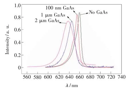
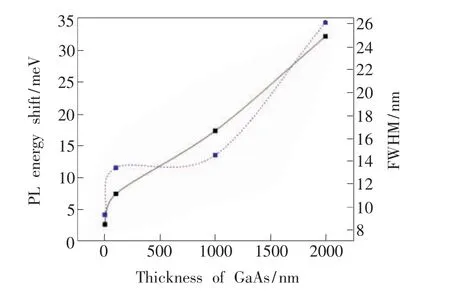
Fig.2 shows the PL spectra of the samples annealed with different thicknesses.From the figure we can see that the blue shift of the sample has a strong correlation with the thickness of the GaAs layer.If we remove the GaAs layer,there is almost no blue shift of the sample.With the increase of GaAs layer thickness,blue shift becomes more obvious under the same annealing time.As is shown in Fig.3,when the thickness of the GaAs layer is 2 μm,its FWHM(full width at half maximum)becomes very large and the quantum well is damaged,so we choose 1 μm as the best thickness of GaAs layer.

Fig.2 PL spectra of the samples annealed with different thicknesses

Fig.3 PL energy shifts and FWHMs obtained for the GaInP/AlGaInP QWs structure as a function of the thicknesses of GaAs at 950℃.The solid line presents the blue shifts.The dot line presents the FWHMs of the blue-shift PL spectra.
3.2 Relationship Between Diffusion Time and PL Energy Shifts
Fig.4 shows the PL energy shifts obtained for the GaInP/AlGaInP QW structure as a function of annealing time with a 1 μm thick GaAs layer at 950℃.In our experiments,the samples exhibit a slight energy shift when annealing for 30 s,and blue shift becomes more and more obvious as the annealing time increases.After corresponding annealing time of 30,60,90,120 s,PL spectrum peak of 662.7 nm shifts continuously to 650.7,635.4,629.4,609.3 nm.As the Fig.5 shows,the full width at half maximum(FWHM)increases because of the quantum well intermixing.

Fig.4 PL spectra of the samples annealed at different time with the thickness of GaAs layer of 1 μm

Fig.5 Changes of the PL blue shift and FWHM at different annealing time.The solid line presents the blue shifts.The dot line presents the FWHMs of the blueshift PL spectra.
3.3 Qualitative Explanation of PL Energy Shifts
In GaAs/AlGaAs material systems,the SiO2layer is believed to enhance inter-diffusion by introducing additional columnⅢ vacancies,VⅢ,at the surface,which quickly diffuses into the bulk and leads to the Al-Ga inter-diffusion.But in the GaInP/AlGaInP material systems,there is basically no effect.So the dominant mechanism for columnⅢself-diffusion in this material involves interstitials rather than VⅢ.In AlGaInP material system,the interstitials are indium atoms.The indium had a higher diffusion coefficient than Ga and led to a similar degree of impurity-induced disordering[14]and the solubility of indium in SiO2is very small,so SiO2doesn't have much effect in the quantum well intermixing.However,indium can easily dissolve in the GaAs[15].The mechanism of the blue-shift in the GaInP/AlGaInP is Al-In interdiffusion.In the high temperature,the In atoms enter the GaAs layer and the Al atoms enter the GaInP layer.It can be seen that the bandgap energy increases as the Al composition increases and the In component decreases,this is in good agreement with the experimental results.
4 Conclusion
In summary,the intermixing behavior of Al-GaInP/GaInP QWs induced by GaAs layer has been investigated.It has found that at the diffusion temperature of 950℃,the best thickness of GaAs layer is 1 μm.With the annealing time increasing the energy gap of AlGaInP/GaInP QW was extending,which created the PL blue shift,and the inter-diffusion of Al and In atoms between QWs and barrier layers contributed to the PL shift,the maximums of the PL blue shift were 171.6 meV.
