Gamma irradiation-induced effects on the properties of TiO2 on fluorine-doped tin oxide prepared by atomic layer deposition
2018-06-27SyedMansoorAliAlgarawiTurkiALKhuraijiAlghamdiMuhammadHammadAzizIsa
Syed Mansoor Ali•M.S.Algarawi•Turki S.ALKhuraiji•S.S.Alghamdi•Muhammad Hammad Aziz•M.Isa
1 Introduction
Among semiconducting oxides,TiO2has received much attention because of its chemical and physical properties such as non-toxicity,stability,wide band gap,high refractive index,permittivity,and high transmittance in the visible region[1,2].TiO2films have three different structural phases:anatase,rutile,and brookite[3–6].Depending on the structural phase,TiO2has different applications such as gas sensors[7],optical cells[8],optical filters[9],solar energy conversion[10],antire flection coatings[11],waveguides[12],photocatalysts[13],and ceramic membranes[14].TiO2is one of the most attractive materials for the window layer in solar cells[15].For solar cell applications,the main requirement of a widegap semiconductor is high optical transmission.The optical electronic transport properties of TiO2strongly depend on the deposition methodology and the structural phase.
Several deposition techniques such as liquid-phase crystaldeposition [16],sol–geldeposition [17,18],hydrothermal deposition[19,20],and electrophoretic deposition[21]have been used to deposit TiO2films.Atomic layer deposition(ALD)has significant advantages over the other methods,such as stoichiometric control,low-temperature processing,precision in material thickness,and self-limiting nature[22].
Oxide semiconductors are highly responsive to gamma radiation.The gamma radiation dissipates as energy into the lattice of the material.In general,gamma radiation interacts with the material in two ways:defect creation and defect annihilation[23].The number of defects created is more than the number of defects annihilated at higher gamma irradiation doses,and vice versa at lower doses[24,25].Interaction with radiations can alter the optical,nanostructural,and electrical properties of thin films[26].In this work,TiO2thin films were deposited on a fluorinedoped tin oxide(FTO)glass substrate by the ALD method,and the modification of the structural,optical,and electrical properties caused by gamma irradiation was studied.
2 Experimental
The TiO2thin films were deposited on FTO substrates using the ALD technique.First,the FTO glass was cleaned by washing with(HCl+H2O2+6 DI)solution and drying under nitrogen(N2) flow.The deposition process for the TiO2thin films involved alternate cycles.The precursors(TiC14and deionized water)were carried into the reaction chamber alternately using N2as the carrier gas under a flow rate of 200 sccm and pressure of 9 hPa.After each precursor cycle,the residual unreacted reactant and the byproduct from the reaction chamber were purged by pure N2gas.The pulse width and the growth rate per cycle were measured to be 0.1 s and 0.4 A˚,respectively.100-nm-thick TiO2thin films were obtained by performing 2500 cycles.
For irradiation,the TiO2films were exposed to a60Co gamma source with a half-life of 5.2714 years,energy of 1.25 MeV,and dose rate of 7.328 kGy/h;the dose was varied between 25,50,75,and 100 kGy.
XRD analysis of the as-deposited and gamma-irradiated samples was performed by using an X-ray diffractometer(Bruker,D8 Discover)with Cu-Kα source radiation.UV–Vis reflectance and transmittance measurements were taken at room temperature using a UV–Vis spectrophotometer(JASCO–V 670)in the wavelength range 200–800 nm.The room-temperature photoluminescence(PL)of the non-irradiated and gamma-irradiated TiO2samples was determined upon excitation at 325 nm using a spectro fluorometer(FP-8200).The impedance spectra were measured by a KEITHLEY 4200 SCS system at room temperature,in air,under dark conditions.
3 Results and discussion
The XRD patterns of the non-irradiated and gammairradiated TiO2films are depicted in Fig.1.It can be clearly seen that the XRD patterns of the TiO2thin films before and after irradiation have plans analogous to FTO,anatase,and rutile.The diffraction patterns agreed well with those of the anatase and rutile phases after removal of the FTO peaks.As the gamma irradiation dose increased,all the peaks became more distinct and shifted to a larger 2θ value.The increase in the peak intensity indicated that the TiO2thin films became highly crystalline as the gamma irradiation dose was increased.The shift in the peaks might be due to the strain produced by gamma irradiation.
The average crystallite size(D),microstrain(μ),and dislocation(δ)of the TiO2films are calculated on the basis of the XRD results,using formulas 1[27],2[28],and 3[29]:

where λ (1.5406 A˚)is the wavelength of the X-ray,θ (°)is the diffraction angle,and β is the full width at half maximum of the peak(radian).
The crystallite size of the films decreased(97–55.7 nm)and the microstrain increased as the gamma irradiation dose was changed from 0 to 100 kGy.The calculated results based on the XRD patterns are given in Table 1.
Figure 2 shows the UV–Vis spectra of the non-irradiated and gamma-irradiated TiO2samples on the FTO substrate.It can be seen that the as-deposited sample shows high transmittance in the visible region,but there is a sudden decrease in transmittance in the ultraviolet region due to the deep absorption.The surface roughness of the thin films had a significant effect,especially in the transparent zone.After gamma irradiation,the roughness of the TiO2thin films led to a decrease in the transmission as a function of the dose.
For crystalline materials,direct transitions are valid according to Tauc’s relation[30].Subsequently,for the present TiO2thin films,only the direct band gap energy was determined by the Tauc linearization(Fig.3).The optical band gap was determined to be 3.31 eV for the asdeposited sample,and it increased to 3.38 eV with an increase in the gamma irradiation dose.This difference may be attributed to the decrease in the particle size or oxygen defect band states formed in the band gap.
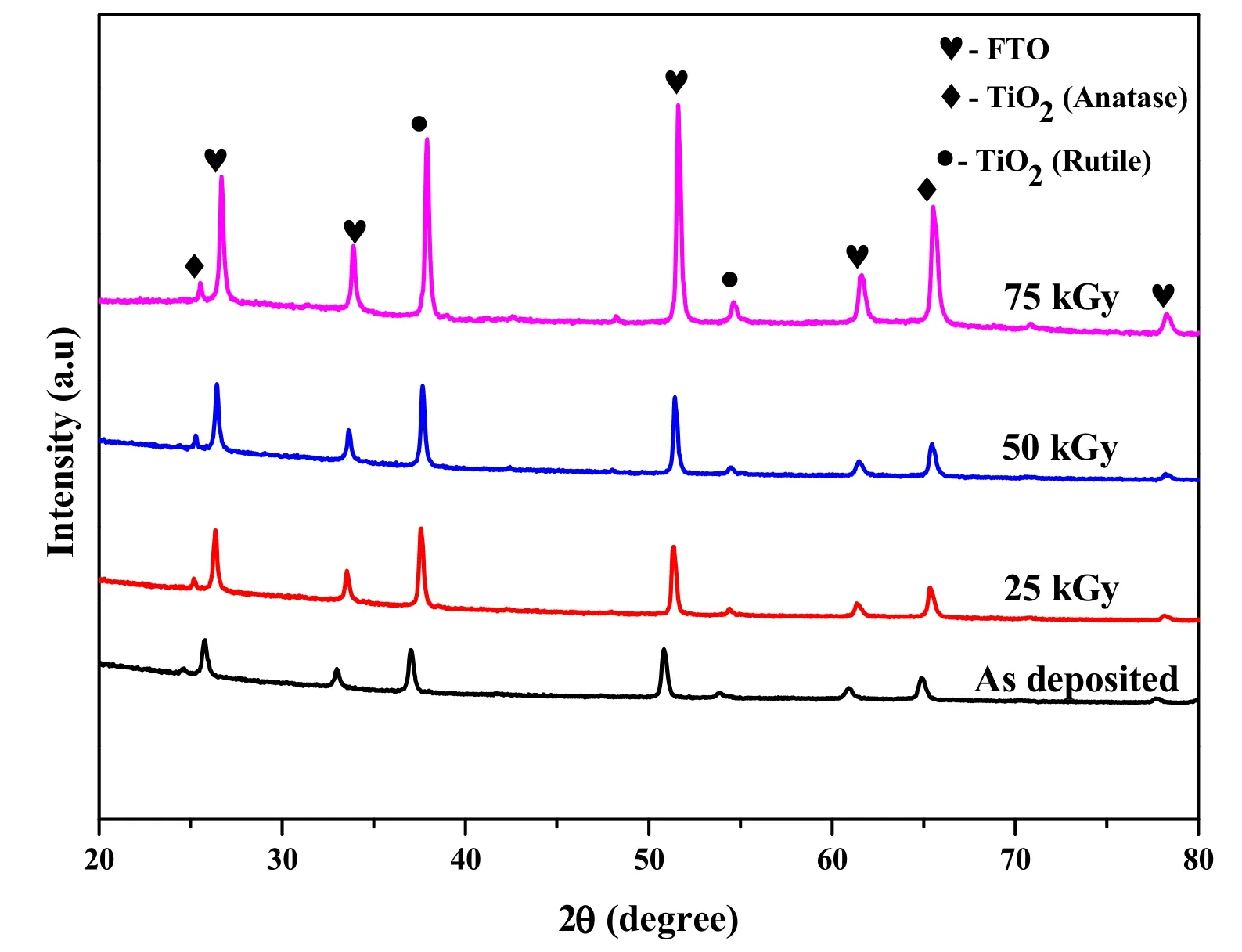
Fig.1(Color online)XRD patterns of TiO2/FTO for different gamma irradiation doses
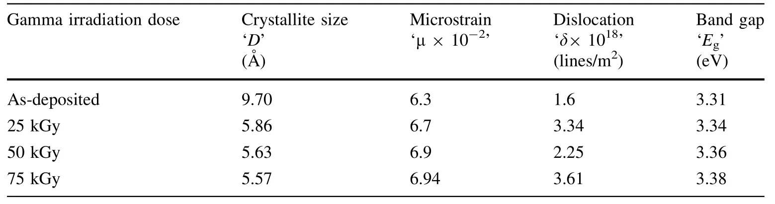
Table 1 Nanostructural parameters and energy band gap of TiO2thin films on FTO glass
Figure 4 depicts the PL spectra of the non-irradiated and gamma-irradiated TiO2thin films for different irradiation doses.It is clear that the gamma-irradiated TiO2films at three different excitation wavelengths(367,378,and 550 nm)and the as-deposited sample show only one excitation(367 nm)[inset of Fig.4].The main excitation at 367 nm was due to the energy band gap emission for the non-irradiated and gamma-irradiated films.Since,the band gaps for the non-irradiated and irradiated samples were calculated from 3.31 to 3.38 eV.The emissions at 378 and 550 nm were lower than the band gaps of the films,implying that the gamma irradiation resulted in additional defect states within the band gap of the TiO2films.The intensity of the band gap and defect emission peaks clearly increased with an increase in the gamma irradiation dose,and the peaks shifted to the longer-wavelength side.The increase in the intensity of the emission peaks of the TiO2film strongly depended on the nanocrystalline structure.The traps in the band gap were probably associated with the intrinsic defects in the TiO2films.The XRD results for the TiO2thin films are favorable for the band gap emission(PL peak).
Frequency-dependent electrical conductivity measurements were taken for the as-deposited and gamma-irradiated TiO2/FTO samples for the charge-transfer and recombination processes.As per the Nyquist plots shownin Fig.5a–d,each sample exhibits a semicircle in the lowfrequency region,which is associated with the electron transport mechanism at the interface between TiO2and FTO.The electron transport resistance decreased with an increase in the gamma irradiation dose.

Fig.2(Color online)Transmission spectra of nonirradiated and gamma-irradiated TiO2thin films

Fig.3(Color online)Tauc’s plot for non-irradiated and gamma-irradiated TiO2thin films

Fig.4(Color online)Photoluminescence spectra of non-irradiated and gammairradiated TiO2thin films
The semicircle fitting of the non-irradiated and gammairradiated TiO2thin films represents a single charge transportation process.The equivalent circuit obtained by the simulation of the experimental data can be seen in Fig.6a,where Rsindicates the contact resistance,RTiO2lFTOindicates the bulk resistance of the films,and Cpdenotes the interface capacitance.The simulated values of all these parameters are obtained using Z-View software and listed in Table 2.
The Bode and phase angle diagrams of the non-irradiated and gamma-irradiated TiO2thin films are shown in Fig.6b.As the peak frequency of the middle semicircle has an inverse relationship with the electron lifetime at the TiO2/FTO interface,the peak frequency increases,indicating a decrease in the lifetime with increased gamma irradiation doses.
4 Conclusion
We investigated the gamma irradiation-induced modification effects on the structure optical and electrical properties of TiO2films deposited by ALD.The XRD results for the irradiated TiO2films revealed an enhancement of the crystallinity.The microstrain and crystallite size increased upon increasing the gamma irradiation dose.The energy band gap and refractive index of the TiO2films,as determined by UV–Vis spectroscopy,increased for the initial dose and then decreased with increasing doses.The two extra peaks after irradiation could be due to the electron captured by the surface defects and the traps produced by the oxygen deficiencies.In the Nyquist plots for each sample,a semicircle appeared in the low-frequency region,which was associated with the charge-transfer process at the TiO2/FTO interface.The charge-transfer resistance decreased with increasing gamma irradiation doses.The electron lifetime of the samples,which was calculated from the Bode phase plot,decreased upon increasing the gamma irradiation doses.

Fig.5(Color online)Nyquist plots for non-irradiated and gamma-irradiated TiO2thin films

Fig.6(Color online)a Equivalent circuit and b Bode plot of non-irradiated and gamma-irradiated TiO2thin films

Table 2 Impedance results for TiO2thin films on FTO glass
1.S.Konstantinidis,J.P.Dauchot,M.Hecq,Titanium oxide thin if lms deposited by high-power impulse magnetron sputtering.Thin Solid Films 515,1182(2006).https://doi.org/10.1016/j.tsf.2006.07.089
2.A.Mills,S.L.Hunte,An overview of semiconductor photocatalysis.J.Photochem.Photobiol.A Chem.108,1(1997).https://doi.org/10.1016/S1010-6030(97)00118-4
3.Z.Wang,U.Helmersson,P.Kall,Optical properties of anatase TiO2thin films prepared by aqueous sol–gel process at low temperature.J.Thin Solid Films 405,50(2002).https://doi.org/10.1016/S0040-6090(01)01767-9
4.S.Richardon,A.Thruston,T.Collette,Identification of TiO2/UV disinfection byproducts in drinking water.J.Environ.Sci.Technol.30,3327(1996).https://doi.org/10.1021/es960142m
5.R.Zhang,L.Gao,Q.Zhang,Photodegradation of surfactants on the nanosized TiO2prepared by hydrolysis of the alkoxide titanium.J.Chemosphere 54,405(2004).https://doi.org/10.1016/S0045-6535(03)00588-5
6.D.G.Shchukin,D.V.Sviridov,Photocatalytic processes in spatially confined micro-and nanoreactors.J.Photochem.Photobiol.C 7,23(2006).https://doi.org/10.1016/j.jphotochemrev.2006.03.002
7.H.Tang,K.Prasad,R.Sanjines,TiO2anatase thin films as gas sensors.Sens.Actuators B 71,26(1995).https://doi.org/10.1016/0925-4005(94)01559-Z
8.B.E.Yoldas,T.W.O’keefee,Antire flective coatings applied from metal–organic derived liquid precursors.J.Appl.Opt.18,3133(1979).https://doi.org/10.1364/AO.18.003133
9.H.Kostlin,G.Frank,G.Hebbinghaus,Optical filters on linear halogen-lamps prepared by dip-coating.J.NonCryst.Solids 218,347(1997).https://doi.org/10.1016/S0022-3093(97)00169-5
10.M.A.Butler,D.S.Ginley,Principles of photoelectrochemical solar energy conversion.J.Mater.Sci.15,1(1980).https://doi.org/10.1007/BF00552421
11.K.Bange,C.R.Ottermann,O.Anderson,Investigations of TiO2films deposited by different techniques.Thin Solid Films 197,279(1991).https://doi.org/10.1016/0040-6090(91)90238-S
12.J.Zhai,T.Yang,L.Zhang,The optical waveguiding properties of TiO2–SiO2composite films prepared by the sol–gel process.Ceram.Int.25,667 (1999).https://doi.org/10.1016/S0272-8842(98)00081-9
13.J.Yu,X.Zhao,Q.Zhao,Photocatalytic activity of nanometer TiO2thin films prepared by the sol–gel method.Mater.Chem.Phys. 69, 25 (2001). https://doi.org/10.1016/S0254-0584(00)00291-1
14.Y.Yan,S.R.Chaudhari,A.Sarkar,Synthesis,characterizations,and optical properties of stacked porous thin films derived from sol–gel process.J.Am.Ceram.Soc.1996,79(1061).https://doi.org/10.1111/j.1151-2916.1996.tb08548.x
15.Y.Chen,E.Stathatos,D.D.Dionysioua,Sol–gel modified TiO2powder films for high performance dye-sensitized solar cells.J.Photochem.Photobiol.A Chem.203,192(2009).https://doi.org/10.1016/j.jphotochem.2009.01.019
16.L.H.Kao,T.C.Hsu,H.Y.Lu,Sol-gel synthesis and morphological control of nanocrystalline TiO2via urea treatment.J.Colloid Interface Sci.316,160(2007).https://doi.org/10.1016/j.jcis.2007.07.062
17.M.Grätzel,Conversion of sunlight to electric power by nanocrystalline dye-sensitized solar cells.J.Photochem.Photobiol.A Chem.164,3(2004).https://doi.org/10.1016/j.jpho tochem.2004.02.023
18.D.Wanga,B.Yua,F.Zhoua,et al.,Synthesis and characterization of anatase TiO2nanotubes and their use in dye-sensitized solar cells.Mater.Chem.Phys.113,602(2009).https://doi.org/10.1016/j.matchemphys.2008.08.011
19.H.Z.Abdullah,C.C.Sorrell,TiO2thick films by electrophoretic deposition.J.Aust.Soc.44(2),12(2008)
20.J.Manríquez,L.A.Godínez,Tuning the structural,electrical and optical properties of Ti(III)-doped nanocrystalline TiO2films by electrophoretic deposition time.Thin Solid Films 515,3402(2007).https://doi.org/10.1016/j.tsf.2006.09.055
21.N.P.Dasgupta,C.Liu,S.Andrews et al.,Atomic layer deposition of platinum catalysts on nanowire surfaces for photoelectrochemical water reduction.J.Am.Chem.Soc.135,12932(2013).https://doi.org/10.1021/ja405680p
22.C.Clayeys,E.Simon,Radiation Effect in Advanced Semiconductor Materials and Devices(Springer,Berlin,2002)
23.S.K.Khamari,V.K.Dixit,T.Ganguli et al.,Effect of60Co gamma-ray irradiation on electrical properties of GaAs epilayer and GaAs p–i–n diode.Nucl.Inst.Methods Phys.Res.B 269,272(2011).https://doi.org/10.1016/j.nimb.2010.11.067
24.E.Tanassova,A.Paskaleva,R.Konakova et al.,In fluence of γradiation on thin Ta2O5-Si structures.Microelectron.J.32,553(2001).https://doi.org/10.1016/S0026-2692(01)00043-X
25.M.Kumari,P.Rana,R.P.Chauhan,Modifications in structural and electrical properties of gamma irradiated CdSe nanowires.Nucl.Inst.Methods Phys.Res.A 753,116(2014).https://doi.org/10.1016/j.nima.2014.03.062
26.C.S.Barret,T.B.Massalski,Structure of Metals(Pergamon Press,Oxford,1980)
27.S.M.Ali,W.A.Farooq,M.R.Baig et al.,Structural and optical properties of pure and Ag doped ZnO thin films obtained by sol gel spin coating technique.Mater.Sci.Pol.33(3),601(2015).https://doi.org/10.1515/msp-2015-0091
28.S.Rani,P.Suri,P.K.Shishodia et al.,Synthesis of nanocrystalline ZnO powder via sol–gel route for dye-sensitized solar cells.Solar Energy Mater.Solar Cells 92,1639(2008).https://doi.org/10.1016/j.solmat.2008.07.015
29.E.A.Davis,N.F.Mott,Conduction in non-crystalline systems V.Conductivity,optical absorption and photoconductivity in amorphous semiconductors.Philos.Mag.22,903(1970).https://doi.org/10.1080/14786437008221061
30.J.Tauc(ed.),Amorphous and Liquid Semiconductors(Plenum Press,London and New York,1974)
杂志排行

Nuclear Science and Techniques的其它文章
- Monte Carlo simulation of incident electrons passing through thin metal layer
- Annual effective dose values from137Cs activity concentrations in soils of Manisa,Turkey
- Preliminary analysis of tritium fuel cycle in Z-pinch-driven fusion– fission hybrid reactor
- Investigation of high-temperature-resistant rhenium–boron neutron shields by experimental studies and Monte Carlo simulations
- Preparation and characterization of Bi2O3/XNBR flexible films for attenuating gamma rays
- Investigation of SPECT/CT cardiac imaging using Geant4