Micromechanics of substrate-supported thin films
2018-04-18WeiHeMeidongHanShibinWangLinAnLiXiuliXue
Wei He·Meidong Han·Shibin Wang·Lin-An Li·Xiuli Xue
1 Introduction
Micro/nano-electromechanical systems are micro/nanometerscale sophisticated devices that integrate electrical and mechanical elements.They are extremely attractive for diverse applications,from optical networks to sensor components,etc.,which can be miniaturized because of their tiny size and weight.Moreover,as an emerging and promising field, flexible electronics have been developed for numerous applications including stretchable integrated circuits,thin film solar cells,and deformable lighting systems[1,2].It is aimed to bring about a revolution in design and implementation of electronics devices,which will satisfy the various essential social needs and to create an amazing human life.Especially,some advanced technologies in optoelectronics,wearable health devices and paper-like displays are demonstrated as follows:
(1)Bio-inspired designs of digital imagers can achieve improved field of view,uniform illumination,and higher precision compared to the conventional planer devices.Figure 1 a presents the magnified view of a hemispherical eye type camera:a curved focal array of silicon photodetectors(yellow pattern)for image capture is integrated with a printed circuit board(green)and a transparent hemispherical cap.The circuit is connected with a computer and the cap supports a planoconvex lens[3].
(2)It is necessary to monitor the state of human health in real time.Many sensors are integrated directly on the human body,which requires them to be thin and flexible.Figure 1b illustrates a stretchable wrist-based phototherapy device.It can follow the hand shape with a large deformation and high fatigue resistance.The blue LEDs are connected by stretchable meanders.Moreover,the complete sensor system is fitted into a textile wrap to enable easy fixation on the hand[4].
(3)Flat-panel displays have experienced explosive development recently and become immensely popular,e.g.the iPad from Apple.However,the displays are often made on glass substrates with a large screen,which can cause problems of fragility and portability.Figure 1c exhibits the conceptual view of a future smart display:a flexible screen with super processors inside that can be rolled up

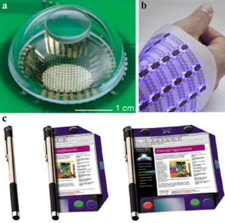
Fig.1 Flexible and stretchable electronics.a Electronic eyeball camera using a hemispherically curved array of silicon photodetectors.Reproduced from Ref.[3],copyright©Nature Publishing Group.b A wrist-based phototherapy device made of stretchable electronics,which allows following the shape of the hand.Reproduced from Ref.[4],copyright©Elsevier.c A conceptual view of a future flexible smart display that can be rolled up into a pen-like device when not in use.Reproduced from Ref.[5],copyright©Nature Publishing Group
Metallic thin films are defined as a solid layer with thickness varying from fractions of a nanometer to several micrometers,although the definition changes depending on the physical properties of interest[6].They are ubiquitous in technologies serving as functional materials,such as electrodes,interconnects,and protective layers.In pursuit of stretchability and supportability,thin films are usually deposited on a substrate by physical/chemical vapor deposition techniques(ion beam sputtering,magnetron sputtering,etc.)[7–9].The obtained thin films can be dense,polycrystalline,and often show in-plane residual stresses up to several GPa.These stresses may arise due to the presence of impurities or voids within the film,partial grain growth or thermomechanical differences between the film and the substrate.An excessive compressive or tensile stress can induce film delamination or cracks leading to a loss of device functionality,or even the failure[10].Noticeably,in some cases,an adhesive film(planar in stress-free state)is attached to a curved substrate such as a spherical one.Then the film experiences compression due to geometric effects and may undergo an instability or wrinkling,which is similar to the unavoidable distortion of distances in planar maps of Earth[11].The basic mechanisms of substrate curvature-induced delamination are extensively studied considering the geometric parameters,mechanical properties,wavelength of wrinkles,etc.[12,13].
During practical applications,film-substrate composites are subject to complex thermo mechanical loadings(diagonal stretching,twisting,bending,compressing,etc.)[14,15],while the substrates may survive a large deformation,the thin metal films may not,which could result in various forms of failure,such as buckling/wrinkling and cracking[16–18].Experimentally,many polymer-supported thin films crack at small elongations(<10%)and their elastic limits are quite small(<1%)[19–21].Moreover,the cyclic loading may cause a BE in the film,leading to a loss of yield strength in reverse direction[22].
When thin films are deposited on a substrate,the film-substrate interface becomes a crucial factor.In poor-bonded films,the cracks accompanied by delamination or buckling may appear early during stretching,while with a 10 nm Cr interlayer enhancing the adhesion between 1µm Cu films and polyimide(Kapton 50HN®by DuPont,12.7µm)substrates,local thinning and debonding of Cu films are observed at strains around 30%with the first micro-cracks appearing at 50%strain[23,24].Since the size of thin films(grain size can be nanometric,<50 nm)is extremely small at least in thickness dimensions,the size effect may play a significant role[25–27].In other words,thin films can behave in a distinct way from their bulk counterparts.In addition,some materials,for instance,obtained by means of PVD technology,do not exist in the bulk state.Accordingly,it is imperative to extract the intrinsic mechanical properties of thin films;however,most of the standard and traditional methods for bulk ones can not be applied directly,particular and dedicated characterization techniques are necessary.
As stated above,to address the mechanics of substrate supported thin films,which are closely related to the performance,reliability and maintainability of many advanced devices[28],is of fundamental importance and poses significant challenges.In this paper,we review ongoing research in the micromechanics of thin films on a substrate.Section 2 describes the interfacial adhesion energy models and how the stress/strain is transferred from the substrate to the film.Section 3 focuses on the techniques of deformation/strain measurements at micro/nanoscale.Section 4 describes the residual stress determination of as-deposited thin films.Section 5 discusses how to extract the film’s intrinsic elastic properties from the film-substrate composites.Section 6 outlines issues of Bauschinger effect under cyclic tests.
2 Interfacial adhesion and stress/strain transfer
For a thin film-substrate structure,the interfacial adhesion is a critical property,which can profoundly influence the mechanical behavior and thus the functionality and dura-bility of advanced devices.For instance,well-bonded Cu films can sustain a tensile strain up to 10%without appreciable cracks,while poor-bonded ones form channel cracks at∼2%strain[23].Depending on the adhesion,spontaneous telephone-cord wrinkles or buckling can appear due to the compressive stresses generated in a polymethylmethacrylate(PMMA)substrate-supported 300 nm thick Al film[29].It is worth mentioning that the regular and parallel straight cracks during deformation could be indicative of a good adhesion[30],and an intermediate layer(Cr,Ti,etc.)is often used to improve the adhesion,which is significant in many cases.
In an attempt to evaluate quantitatively the adhesion between thin films and substrates,adhesion energy,defined in terms of fracture mechanics as the minimum energy per unit area required to create new surfaces,is proposed.Many relevant experimental methods have been developed for films adherent to rigid substrates,such as indentation,scratch test,peel test,and time-of-flight secondary ion mass spectroscopy[31,32].Nevertheless,those techniques may not be applicable to films on flexible substrates considering the viscoelasticity of polymer substrates.It is well known that the adhesion energy can be derived from the buckle’s geometric parameters of thin films as proposed by Hutchinson and Suo[33].Particularly,Cordill et al.[34]developed a new energy balance model to determine the adhesion energy of thin films on compliant polyimide substrates by measuring the dimensions of buckles induced by the fragmentation test.Various Cr films of thickness∼50−190 nm were well examined,and this model was successfully applied to 20 nm thick CoFeB thin films deposited on Kapton®substrates with the measured adhesion energy of5.4 J/m2[35].Noticeably,their model was more suitable for very thin films(<200 nm)and restricted to a single layer,and Wu et al.[36]further modified and extended it to evaluate the adhesion energy of∼1µm thick nanostructured multilayer films(different modulation periods)on a flexible substrate.The buckle dimensions can be obtained using atomic force microscope(AFM),digital microscope[29,37],and white light interferometry,etc.
Herein,the model proposed by Cordill et al.[34]is briefly described below:in stretching the film/polymer composites,the channel cracks perpendicular to the tensile direction(xdirection)will first appear at lower strains(Fig.2a).During further straining of the film,the crack density increases,and a compressive transverse stress in the film strips increases due to the Poisson’s ratio mismatch between the film and the substrate.The compressive stresses will then cause the formation of buckles,which crack at their apex with the buckle width extending in the transverse direction(y-direction).The buckling mode can be regarded as “Euler-mode”with a strip clamped at both ends(between channel cracks).Figure 2b schematically illustrate the buckle dimensions strongly related to the adhesion energy,e.g.the heightδand width 2b.

Fig.2 a Illustration of the top surface of a cracked and buckled film under tension.b Schematic cross-section of a buckle.Reproduced from Ref.[29],copyright©Elsevier
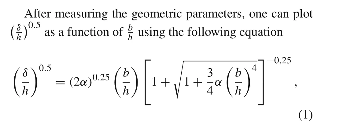
wherehdenotes the film thickness,αis the obtained fitting parameter relevant to the adhesion energyΓ:

whereEandνrespectively represent the Young’s modulus and Poisson’s ratio of the film.
On the other hand,during uniaxial stretching,the stress/strain of a thin film is usually transferred from the substrate through interface,since there is no direct force exerted on the film.The Poisson’s ratio mismatch between two layers provokes a slight curvature of the composite structure in the plane orthogonal to the tensile direction.However,considering the tiny film thickness compared to the substrate and for the purpose of simplicity,the average strains over the film thickness and over the substrate thickness are used with the hypothesis of a flat specimen.Furthermore,it is often assumed that the interface is perfect and the deformation is continuous through the film-substrate interface,in other words,the average strain of the film is indistinguishable compared to the one of the substrate.These assumptions are of vital importance since they are the basis of many mechanical theories and methods,such as the adhesion model[34]and the rule of mixture].Some perceptive experiments have been done in an effort to justify these hypotheses.By means of X-ray diffraction and some other deformation measurement techniques,a complete strain transfer throughcase of a thin Ni/polyimide(PI)/Cu multilayer studied by X-ray tensile testing,it is concluded that only part of the elastic strain in Ni is transferred to Cu,and PI has no effect on the elastic stress transfer behavior[42,43].
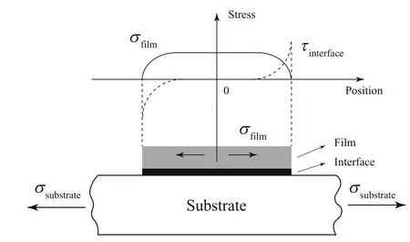
Fig.3 Schematic of the shear lag model:the film undergoes strain as a result of the substrate induced stresses that are transferred across the interface.The shear stress in the interface reaches a maximum at the ends of the film and zero closing to the center.From equilibrium,the tensile stress in the film,which is zero near the edges and increases to a maximum towards the center,can be determined from the accumulation(integration)of interfacial shear stress
With a fully bonded interface,how the stress is transferred from the substrate to the film is of interest and crucial importance.Yin and Prieto-Munoz[44]derived a general elastic solution for multilayered materials,and Faurie et al.[45]proposed a mechanical approach to determine the stresses generated into the film.Herein,it is worth mentioning the shear lag model concerning stress transfer and cracking.Figure 3 schematically shows a thin film coated on a strained substrate,the ends of the film are not directly pulled in tension,i.e.free surfaces.Consequently,any stress the film experiences can only be transferred across the adhering interface.This implies the existence of an interfacial shear stress that accumulates from the ends of the film inward to cause a uniaxial tension,and the tensile stress in the film must be built from zero at the ends to an equilibrium value towards the middle[46].When the applied load grows and the film stress near the center exceeds a critical value,a crack will appear and new free surfaces are introduced.The film is then split into two segments with smaller length.This causes a stress relief in the film.When the load keeps increasing,new cracks will occur midway in the same manner.As this process continues much further,the length of each new segment becomes tiny and the shear stresses at both ends of the segment begin to overlap,which results in their partial balance,or in other words,the magnitude of the loading transferred across the shear lag region falls below the critical value,thereby limiting further crack generation,which is known as crack saturation.Moreover,a modification to the shear lag model is proposed to take into account the residual strains[47].It should be noted that even with numerous cracks,all the segments of the film are assumed to be adherent to the substrate everywhere,and the substrate strain in the zone of the crack gaps is larger compared to the continuous composite,since only the substrate experience the load in the uncoated region.
3 Deformation/strain measurement


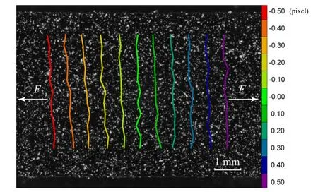
Fig.4 Displacement field at a given force.A random speckle pattern was created by spraying the white paints on the specimen surface.The linear displacement distribution is clear from the uniform vertical contour lines


Figure 4 shows an example of the displacement field of a Kapton®substrate under in situ tension.The vertical contour lines indicate a linear displacement distribution that is expected for a perfect uniaxial tensile testing,and the corresponding uniform strain field can reach a precision up to 10−4.
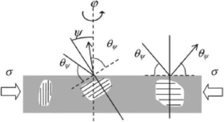
Fig.5 Concept of diffraction strain analysis.When a polycrystal is subject to a uniaxial compression parallel to the surface,the lattice spacing of{hkl}planes varies depending on their orientations with respect to the loading direction.This lattice strain can be measured by X-ray diffraction and its direction,i.e.the direction of the diffraction vector,is identified by the angles ϕ and ψ ,where ϕ is the rotation angle of the specimen about the surface normal and ψ is the angle between the normal to the diffraction planes and the surface normal.Reproduced from Ref.[49]
Noticeably,the above techniques acquire true strains,while one phase selective,non-contact and non-destructive method,i.e.X-ray diffraction(XRD),only captures the elastic strains of metallic thin films.Combined with XRD and DIC,many mechanical properties can be studied,as will be discussed later.When a polycrystalline film is irradiated with X-rays,the diffraction angle 2ϑhkl,at which the maximum or centroid diffracted intensity is determined,can be measured for each{hkl}diffraction plane.Because of the presence of stress,the interplanar spacingdhklof the lattice planes{hkl}depends on the orientations of constituent crystallites with respect to the specimen frame of reference.For instance,if a polycrystalline material is subject to a compressive stress parallel to the surface,as shown in Fig.5,{hkl}planes parallel to the surface are extended,while planes normal to the surface are compressed[54].
With the Bragg’s law:λ=2dhklsinϑhkl,the spacing is obtained with the Bragg’s angleϑhkland X-ray wavelengthλ.The principle of strain measurement is to take the lattice spacing as a gage

where(d0)hklis the stress-free spacing.The strain can be considered as uniform on the macroscopic scale,producing a shift of the diffraction peak,while the non-uniform microstrain due to the lattice distortion can cause a broadening of the diffraction peak.Although the strain precision may be influenced by many factors(X-ray intensity,collimator alignment,etc.),generally,10−4is attainable.
4 Residual stress
Residual stress is almost always present in thin films deposited on substrates.From the definition“the self-equilibrating internal stresses existing in a free body at equilibrium with no externally imposed surface traction”,one should notice that residual stresses must be equilibrated and intrinsic to the same body[55].The evaluation techniques could be classified into non-destructive and destructive or semi-destructive methods.
4.1 Non-destructive techniques
4.1.1 Curvature method(Stoney’s formula)
Thin films deposited on a flat substrate can lead to a curvature of the substrate due to the residual stresses.In 1909,Stoney[56]firstly derived an expression for the curvature of a steel strip caused by the stresses in a metallic coating,which is known as Stoney’s formula.This equation is based on several assumptions,and has been extended and widely used for predicting stresses in coatings from the curvature of the substrate,such as the extended Stoney’s equation for thin substrate and the one in the case of spatially non-uniform curvature[57,58].After assuming the elastic linearity and isotropy of both film and substrate,much smaller film thickness than the substrate thickness,equal-biaxial stress state,etc.,the most basic form of Stoney’s formula can be written as follows

whereEs/(1−νs)is the biaxial modulus of the substrate,hsandhfare the thickness of substrate and film respectively,RiandRfthe curvature radii before and after film deposition.
It is important to note that if the substrate is relatively compliant with the film highly deformed beyond the linear-elastic range,and if the film thickness is relatively large,Stoney’s formula is not directly applicable[59].For example,when a thin metal film is deposited on a polyimide substrate experiencing high compressive stresses,the common spherical shape would be transformed into a cylindrical shape,which is known as the curvature bifurcation[60].
4.1.2 Sin2ψ method(XRD)
As previously mentioned,XRD technique uses the interplanar lattice spacing as an “atomic strain gage”to measure strains.The residual elastic strains are determined as the relative change of this spacing with respect to the one in stress-free state.This allows the residual stress state to be readily calculated using the appropriate form of Hooke’s law depending on the elastic properties(macroscopic isotropy or anisotropy)of thin films[61–63].However,the calculated mechanical elastic constants should be carefully taken into consideration,since they are strongly dependent on the type and sharpness of texture,the number of randomly oriented crystallites in the polycrystalline aggregate and the assumed grain interaction model[64–66].
4.2 Destructive or semi-destructive methods
There are many residual stress evaluation approaches involving material removal or machining[67–70].All of these methods rely on the same principle:when new traction-free surfaces are created within the sample,a redistribution and re-equilibration of strains can be measured to obtain the preexisting residual stress state in terms of a finite element(FE)or analytical model.For instance,as can be seen in Fig.6[71],an annular trench of 3µm inner diameter was incrementally milled with a focused ion beam(FIB)around the Pt-coated region(the central pillar with a patterned surface),and a sequence of SEM micrographs of the patterned area was acquired before and after each milling step.The average stress in the pillar volume can be calculated from the elastic modulus and Poisson’s ratio by knowing the average strain at the maximum depth with the DIC strain measurements.It is interesting to note that a significant stress gradient through the coating thickness can also be characterized.
5 Elastic properties determination
As mentioned above,specific techniques are required to scrutinize the individual mechanical properties of substrate supported thin films.For instance,substrate/wafer curvature to study the stress evolution during thermal cycling[72]or to obtain the isothermal film stresses[73],electrical resistance method[35,74]to acquire the crack initiation,indentation to measure the hardness and elastic modulus[75–77],bulge test to obtain the yield strength[78],combined synchrotron XRD and biaxial tensile testing to extract the yield surface[79],etc.In this section,we focus interest on the elastic constants determination of thin films,which can be classified into two categories:static and dynamic techniques.
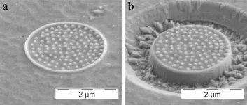
Fig.6 Scanning electron microscope(SEM)images of the patterned area acquired before and after milling.The strain relief can be measured by means of DIC.Reproduced from Ref.[66],copyright©Elsevier
In static techniques,small-scale tensile testing is often combined with other methods to address the elastic properties of substrate-supported thin films.After assuming a uniform one-dimensional(1D)tensile stress distribution within the film thickness,one can subtract the contribution of substrate from the composite stress–strain curves to obtain the individual thin film’s mechanical behavior,which is known as the rule of mixture[39,80,81].In their work,Chen et al.[82]examined its validity for different sample geometries and loading configurations by determining the three-dimensional(3D)elastic stress field in a composite structure.This approach is an ingenious and simple way to extract the elastic properties,nevertheless,several factors should be considered,such as the interfacial adhesion,film microstructure and surface curvature.Recently,based on the rule of mixture,we propose an original procedure to determine the in-plane elastic modulus of thin films[83].Tungsten films,400 nm thick,were coated on both sides of a dogboneshaped Kapton®substrate over half of the gage length to eliminate the surface curvature influence(Fig.7).By means of our custom-designed dual DIC system,the macroscopic strain of coated and uncoated components can be measured simultaneously during a tensile testing.From the strain difference,the Young’s modulus of thin films can be acquired using the following equation


X-ray tensile testing is another well-known method.In their work,Hommel et al.[41]studied cyclic deformation of 700 nm thick Cu films on Kapton®substrates in tension and compression.The elastic strain in the film was measured by XRD,and the true strain of the substrate was obtained with an external strain gage attached to its backside.Up to∼0.1%in tension,the elastic strain is identical to the true strain showing a fully bonded interface.When continuing stretching,a clear deviation appears,which indicates the initiation of a plastic deformation.This is reasonable since elastic strain will be smaller than true strain when inelastic deformation occurs.With Hooke’s law,the film stresses can be acquired and the role of strain hardening can be quantitatively investigated[21].This method was further developed by combining synchrotron XRD and DIC to study elastic properties of ultra-thin films[20].However,it is significantly contingent upon the strong interfacial adhesion considering the fact that the deviation could originate from the poor adhesion rather than the inelastic deformation.The effort may be put into measuring both elastic and true strains of films.Furthermore,Faurie et al.[45,84]developed a mechanical description of film-substrate composite and analytical solutions for XRD strain analyses including texture and grain interaction models,which can be applied to extract the elastic constants of fiber-textured or non-textured thin films.
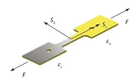
Fig.7 Schematic illustration of one substrate with films coated on both sides and half surface.The left section is films/substrate composite,and the right part is the uncoated substrate.Reproduced from Ref.[78],copyright©Elsevier
In dynamic techniques,resonant ultrasound spectroscopy and impulse excitation technique[85,86]are immensely popular.The work of Slim et al.[87]has reviewed the models well,including Lopez’s model and Pautrot’s model,to determine the films’elastic modulus in the impulse excitation technique,and they also evaluate their accuracy and precision based on experiments,as well as comparing with a finite element model.For a 0.98 mm thick stainless steel coated with 6.7µm thick Al film,they excite the substrate by an impulse,and the acoustic vibrations are recorded.Subsequently,the frequency can be used in a mechanical model to obtain the Young’s modulus of thin films.
6 Cyclic deformation/Bauschinger effect(BE)
The mechanical behavior of a metallic material depends not only on its stress state,but also on its deformation history.The plastic deformation in one direction can affect subsequent plastic response in the reverse direction.One consequence is that an increase in tensile yield strength occurs at the expense of a reduction in compressive yield strength.This specific mechanical response evidenced in bulk polycrystalline materials is known as the BE[88].
Figure 8 schematically shows this effect on a typical stress–strain curve.The stress,σyis the yield stress,σfthe forward flow stress,andσrcorresponding to the yield stress on the reverse loading.The material is firstly loaded in tension and yields at pointA.After stretching to pointB,the loading direction is reversed.Unloading occurs along the elastic line until yielding.If there is no directionality effect,i.e.isotropic hardening,the material will start flowing plastically at a stress equal toσf(pointE),then reload along a linear line starting from pointF.The idealized curve is shown in dashed lines(the sequenceO–A–B–E–F).However,the material exhibiting the BE will have a lower reverse yield stress(σr<σf),and the loading path followsO–A–B–C–D.It should be noted that the loss of the reverse yield stress may be equal to the growth of the forward yield stress(|σr|+σf=2σy),which is referred to as the kinematic hardening.The BE is generally ascribed to either short-range effects or to long-range effects,such as the dislocation pile-ups and tangles at grain boundaries.
In practical use,thin films are submitted to multiple strain cycles.This arises great interest to verify whether the BE also appears in metallic thin films,since the loss of strength in the reverse direction may cause serious failure.Moreover,the nanometric length scale in such systems could influence their plastic responses.
It is straightforward to scrutinize the BE using cyclic testing in tension and compression,which has been well established for bulk materials.However,this is much more difficult for thin film-substrate composites.To apply a compressive stress relative to the original as-deposited film state is very challenging due to their tiny thickness/lateral dimension ratio causing an overall flexural deformation,while to obtain the individual stress–strain curves of thin films in both tensile and compressive strain regime is even more complicated.
Although there are many experimental techniques,as mentioned above,on the plasticity of thin metal films,only a very few were successfully exploited to study the BE.Based on the substrate curvature method,Baker et al.[89]studied the thermomechanical behavior of passivated thin Cu films on Si substrates.In this technique,the changes in substrate curvature during thermal cycles with varying temperature endpoints were used to calculate the film stresses.When small amounts of oxygen were added to a Cu film in the deposition process,a Bauschinger-like effect was observed.Nevertheless,it is difficult to interpret due to the change of temperature.Work by Xiang and Vlassak[22]reported the direct experimental evidence of a strong BE in thin metal films under isothermal conditions.They developed a new technique to measure the cyclic stress–strain curve based on the plane-strain bulge test method.It is concluded that passivated films exhibit a significant BE even when the applied stress is still in tension,while unpassivated or freestanding films show little or no reverse flows.This was explained as follows:for the film-passivation composites,a boundary layer with high dislocation density forms at the interface causing a high back stress which facilitates the earlier reverse plastic flow;for a freestanding film,many dislocations can exit the film because of the free surfaces,and no back stresses are generated.In addition,since the interface is an obstacle to the motion of dislocations,it is believed that a plastic strain gradient is introduced nearby.Thus,the strain-gradient plasticity theory was applied to describe the effects of film thickness on the plasticity of passivated Cu films,but failed to address the BE[90].It is interesting to point out that Brugger et al.[91]presented a two-dimensional(2D)strain gradient plasticity finite-element model involving grain boundaries which agrees well with the experimental results obtained by Xiang and Vlassak[90].Unfortunately,the BE was not taken into account.

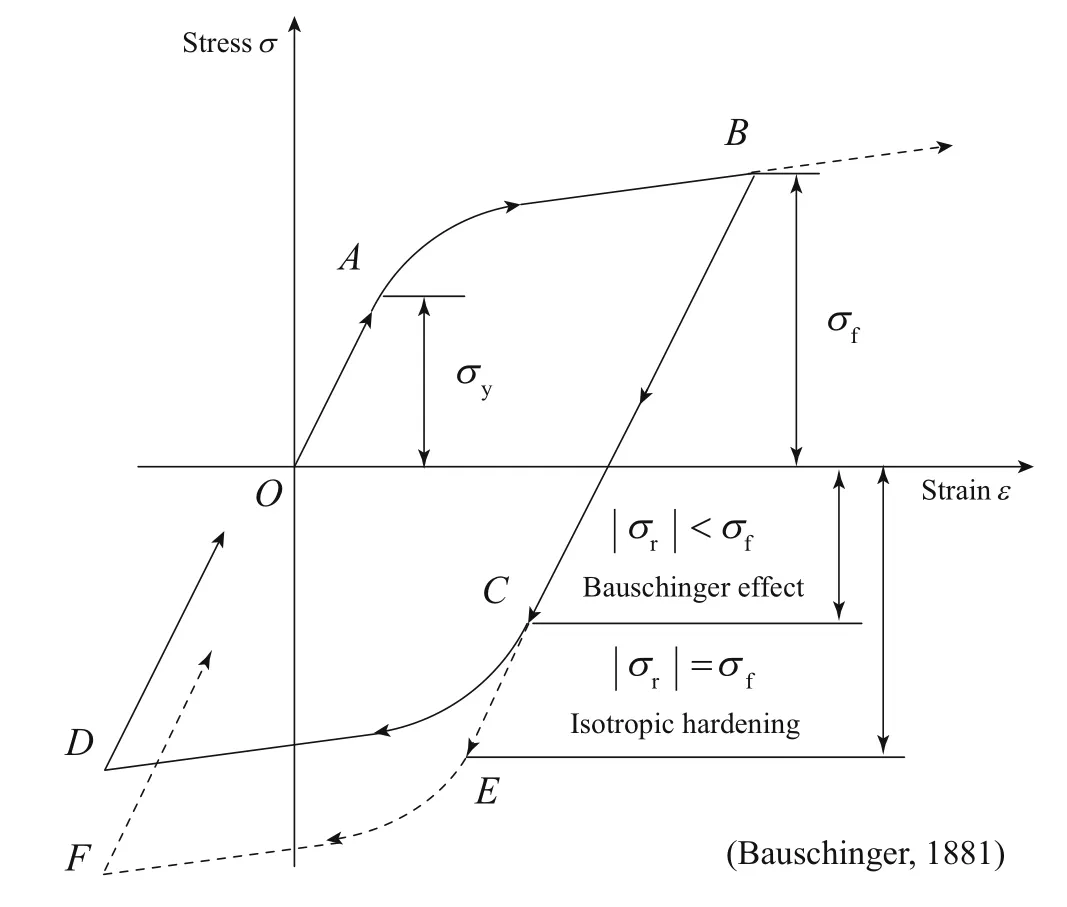
Fig.8 Schematic illustration of the BE existing in many metallic materials with coarse grains[88]
Regretfully,no experimental study of BE on polymersupported thin metal films has been reported which may be due to the considerable technical complexity.Nonetheless,the developing pre-stretching technique would contribute to that research.It is highly popular in geometric transformation of 2D micro/nanostructures into extended 3D layouts[99–101].The principle is to bond 2D structures to the adhesion sites of a uni/biaxially pre-stretched elastomer substrate,and then the compression induced by relaxing the pre-strain in the substrate results in coordinated out-of-plane buckling,bending,twisting,etc.yielding 3D structures.Similar to this method,Renault et al.[102]prestretched a compliant polyimide substrate by a uniaxial tensile tester inside the vacuum deposition chamber.Ultra-thin gold films were then coated while retaining the pre-strain of the substrate.After deposition,both compressive and tensile stresses relative to the as-deposited residual stress state can be applied to the films,and Faurie et al.[103]performed the X-ray strain analyses ofa{111}fiber-textured gold film under compression.However,both the tensile tester and the deposition machine will be irreversibly damaged using this technique,especially for the electrical components even with an extra protection.Furthermore,only one specimen can be obtained during the film deposition so that ensuring the experimental repeatability is difficult.A novel pre-stretching technique is greatly desired to perform cyclic tests for the BE study[104].
7 Concluding remarks
Substrate-supported thin films provoke great interest either for academic research:to understand better the mechanical responses of micro/nanoscale materials or for practical applications such as the stretchable devices.This review article has presented an overview of recent efforts aimed at the investigation of fundamental mechanics and characterization techniques of thin films.The models to determine the interfacial adhesion energy and stress/strain transfer through interface has been described.We also discuss the specific methods to measure film deformation,residual stresses and elastic properties.Particularly,the BE in thin films on rigid substrates has been demonstrated.Regretfully,experimental BE study on compliant substrate-supported thin films,to the best of our knowledge,is still deficient.It is hoped that this review could shed insights into the further research on the mechanics of thin films.
AcknowledgementsThis work was supported by the National Natural Science Foundation of China(Grants 11472186 and 11602083)and the Natural Science Foundation of Hunan Province,China(Grant 2016JJ6044).
1.Crawford,G.:Flexible at Panel Displays.Wiley,Somerset(2005)
2.Kim,D.-H.,Xiao,J.,Song,J.,et al.:Stretchable,curvilinear electronics based on inorganic materials.Adv.Mater.22,2108–2124(2010)
3.Ko,H.C.,Stoykovich,M.P.,Song,J.,et al.:A hemispherical electronic eye camera based on compressible silicon optoelectronics.Nature 454,748–753(2008)
4.Brand,J.,Kok,M.,Koetse,M.,et al.:Flexible and stretchable electronics for wearable health devices.Solid-State Electron.113,116–120(2015)
5.Forrest,S.:The path to ubiquitous and low-costorganic electronic appliances on plastic.Nature 428,911–918(2004)
6.Fewster,P.:X-ray analysis of thin films and multilayers.Rep.Prog.Phys.59,1339(1996)
7.Cotton,D.,Graz,I.,Lacour,S.:Stretchable touch sensitive keypad.Proc.Chem.1,152–155(2009)
8.Rogers,J.,Someya,T.,Huang,Y.:Materials and mechanics for stretchable electronics.Science 327,1603–1607(2010)
9.Kim,D.-H.,Ahn,J.-H.,Choi,W.M.,et al.:Stretchable and foldable silicon integrated circuits.Science 320,507–511(2008)
10.Freund,L.,Suresh,S.:Thin Film Materials:Stress,Defect Formation and Surface Evolution.Cambridge University Press,Cambridge(2004)
11.Hohlfeld,E.,Davidovitch,B.:Sheeton a deformable sphere:wrinkle patterns suppress curvature-induced delamination.Phys.Rev.E 91,012407(2015)
12.Bella,P.,Kohn,R.V.:Wrinkling of a thin circular sheet bonded to a spherical substrate.Philos.Trans.R.Soc.A 375,2093(2017)
13.Hure,J.,Roman,B.,Bico,J.:Stamping and wrinkling of elastic plates.Phys.Rev.Lett.109,054302(2012)
14.Kim,D.-H.,Song,J.,Choi,W.,et al.:Materials and noncoplanar mesh designs for integrated circuits with linear elastic responses to extreme mechanical deformations.Proc.Nat.Acad.Sci.105,18675–18680(2008)
15.Song,J.,Feng,X.,Huang,Y.:Mechanics and thermal management of stretchable inorganic electronics.Natl.Sci.Rev.3,128–143(2016)
16.Toth,F.,Rammerstorfer,F.,Cordill,M.,et al.:Detailed modelling of delamination buckling of thin films under global tension.Acta Mater.61,2425–2433(2013)
17.Li,B.,Cao,Y.,Feng,X.,et al.:Mechanics of morphological instabilities and surface wrinkling in soft materials:a review.Soft Matter 8,5728–5745(2012)
18.Xue,X.,Wang,S.,Zeng,C.,et al.:Buckling-delamination and cracking of thin titanium films under compression:experimental and numerical studies.Surf.Coat.Technol.244,151–157(2014)
19.Huang,H.S.,Pei,H.J.,Chang,Y.C.,et al.:Tensile behaviors of amorphous-zrcu/nanocrystalline-cu multilayered thin film on polyimide substrate.Thin Solid Films 529,177–180(2013)
20.Djaziri,S.,Renault,P.-O.,Le Bourhis,E.,et al.:Comparative study of the mechanical properties of nanostructured thin films on stretchable substrates.J.Appl.Phys.116,093504(2014)
21.Hommel,M.,Kraft,O.:Deformation behavior of thin copper films on deformable substrates.Acta Mater.49,3935–3947(2001)
22.Xiang,Y.,Vlassak,J.:Bauschinger effect in thin metal films.Scr.Mater.53,177–182(2005)
23.Xiang,Y.,Li,T.,Suo,Z.,et al.:High ductility of a metal film adherent on a polymer substrate.Appl.Phys.Lett.87,161910(2005)
24.Lu,N.,Wang,X.,Suo,Z.,et al.:Metalfilmson polymer substrates stretched beyond 50%.Appl.Phys.Lett.91,221909(2007)
25.Niu,R.M.,Liu,G.,Wang,C.,et al.:Thickness dependent critical strain in submicron cu films adherent to polymer substrate.Appl.Phys.Lett.90,161907(2007)
26.Marx,V.,Cordill,M.,Tbbens,D.,et al.:Effect of annealing on the size dependent deformation behavior of thin cobalt films on flexible substrates.Thin Solid Films 624,34–40(2017)
27.Graudejus,O.,Jia,Z.,Li,T.,et al.:Size-dependent rupture strain of elastically stretchable metal conductors.Scr.Mater.66,919(2012)
28.Suo,Z.,Vlassak,J.J.,Wagner,S.:Micromechanics of macroelectronics.China Particuol.3,321–328(2005)
29.Jia,H.,Wang,S.,Li,L.,et al.:Application of optical 3d measurement on thin film buckling to estimate interfacial toughness.Opt.Lasers Eng.54,263–268(2014)
30.Mittal,K.:Adhesion measurement of thin films.Act.Passive Electron.Compon.3,21–42(1976)
31.Gerberich,W.,Cordill,M.:Physics of adhesion.Rep.Prog.Phys.69,2157(2006)
32.Chen,J.,Bull,S.:Indentation fracture and toughness assessment for thin optical coatings on glass.J.Phys.D Appl.Phys.40,5401(2007)
33.Hutchinson,J.W.,Suo,Z.:Mixed mode cracking in layered materials.Adv.Appl.Mech.29,63–191(1991)
34.Cordill,M.,Fischer,F.,Rammerstorfer,F.,et al.:Adhesion energies of cr thin films on polyimide determined from buckling:experiment and model.Acta Mater.58,5520–5531(2010)
35.Faurie,D.,Zighem,F.,Garcia-Sanchez,A.,et al.:Fragmentation and adhesion properties of cofeb thin films on polyimide substrate.Appl.Phys.Lett.110,721(2017)
36.Wu,K.,Zhang,J.Y.,Liu,G.,et al.:Buckling behaviors and adhesion energy of nanostructured Cu/x(x=Nb,Zr)multilayer films on a compliant substrate.Acta Mater.61,7889(2013)
37.Wu,D.,Xie,H.,Yin,Y.,et al.:Micro-scale delaminating and buckling of thin film on soft substrate.J.Micromech.Microeng.23,03540(2013)
38.Mohri,M.,Nili-Ahmadabadi,M.,PouryazdanPanah,M.,et al.:Evaluation of structure and mechanical properties of Ni-rich NiTi/Kapton composite film.Mater.Sci.Eng.A 668,13–19(2016)
39.Kirsch,B.,Chen,X.,Richman,E.,et al.:Probing the effects of nanoscale architecture on the mechanical properties of hexagonal silica/polymercomposite thin films.Adv.Funct.Mater.15,1319–1327(2005)
40.Geandier,G.,Renault,P.-O.,Le Bourhis,E.,et al.:Elastic-strain distribution in metallic film-polymer substrate composites.Appl.Phys.Lett.96,041905(2010)
41.Hommel,M.,Kraft,O.,Arzt,E.:A new method to study cyclic deformation of thin films in tension and compression.J.Mater.Res.14,2373–2376(1999)
42.Schadler,L.,Noyan,I.C.:Experimental Determination of the Strain Transfer Across a Flexible Intermediate Layerin Thin Film Structures as a Function of Flexible Layer Thickness//MRS Proceedings.Cambridge University Press,Cambridge(1991)
43.Schadler,L.,Noyan,I.:Experimental determination of the strain transfer across a flexible intermediate layerin thin-film structures.J.Mater.Sci.Lett.11,1067–1069(1992)
44.Yin,H.,Prieto-Munoz,P.:Stress transfer through fully bonded interface of layered materials.Mech.Mater.62,69–79(2013)
45.Faurie,D.,Renault,P.-O.,Le Bourhis,E.,et al.:Determination of elastic constants of a fiber-textured gold film by combining synchrotron X-ray diffraction and in situ tensile testing.J.Appl.Phys.98,093511(2005)
46.Wojciechowski,P.,Mendolia,M.:Fracture and cracking phenomena in thin films adhering to high-elongation substrates.Phys.Thin Films 16,271–340(1991)
47.Yanaka,M.,Tsukahara,Y.,Nakaso,N.,et al.:Cracking phenomena of brittle films in nanostructure composites analysed by a modified shear lag model with residual strain.J.Mater.Sci.33,2111–2119(1998)
48.Huang,H.,Spaepen,F.:Tensile testing of free-standing Cu,Ag and Al thin films and Ag/Cu multilayers.Acta Mater.48,3261–3269(2000)
49.Belrhiti,Y.,Gallet-Doncieux,A.,Germaneau,A.,et al.:Application of optical methods to investigate the non-linear asymmetric behavior of ceramics exhibiting large strain to rupture by fourpoints bending test.J.Eur.Ceram.Soc.32,4073–4081(2012)
50.Wu,D.,Xie,H.,Dai,X.,etal.:Anovel method to fabricate microgratings applied for deformation measurement around a crack in a thin film.Meas.Sci.Technol.25,025012(2014)
51.Hild,F.,Roux,S.:Digital image correlation:from displacement measurement to identification of elastic properties—a review.Strain 42,69–80(2006)
52.Duprfie,J.,Doumalin,P.,Husseini,H.,et al.:Displacement discontinuity or complex shape of sample:assessment of accuracy and adaptation of local dic approach.Strain 51,391–404(2015)
53.Barranger,Y.,Doumalin,P.,Duprfie,J.,et al.:Strain measurement by digital image correlation:influence of two types of speckle patterns made from rigid or deformable marks.Strain 48,357–365(2012)
54.Welzel,U.,Ligot,J.,Lamparter,P.,et al.:Stress analysis of polycrystalline thin films and surface regions by X-ray diffraction.J.Appl.Crystallogr.38,1–29(2005)
55.Noyan,I.,Huang,T.,York,B.:Residual stress/strain analysis in thin films by X-ray difiraction.Crit.Rev.Solid State Mater.Sci.20,125–177(1995)
56.Stoney,G.:The tension of metallic films deposited by electrolysis.Containing papers of a mathematical and physical character.Proc.R.Soc.Lond.Ser.A 82,172–175(1990)
57.Chou,T.-L.,Yang,S.-Y.,Chiang,K.-N.:Overview and applicability of residual stress estimation of film-substrate structure.Thin Solid Films 519,7883–7894(2011)
58.Janssen,G.,Abdalla,M.,Van Keulen,F.,et al.:Celebrating the 100th anniversary of the stoney equation for film stress:developments from polycrystalline steel strips to single crystal silicon wafers.Thin Solid Films 517,1858–1867(2009)
59.Zhu,J.,Xie,H.,Hu,Z.,et al.:Residual stress in thermal spray coatings measured by curvature based on 3d digital image correlation technique.Surf.Coat.Technol.206,1396–1402(2011)
60.Kim,C.,Lee,T.-I.,Kim,M.,et al.:Warpage analysis of electroplated cu films on fiber-reinforced polymer packaging substrates.Polymers 7,985–1004(2015)
61.Culity,B.:Elements of X-ray Diffraction.Addition-Wesley,London(1978)
62.Hauk,V.:Structural and Residual Stress Analysis by Nondestructive Methods:Evaluation-Application-Assessment.Elsevier,Amsterdam(1997)
63.Noyan,I.,Cohen,J.:Residual Stress:Measurement by Diffraction and Interpretation.Springer,New York(1987)
64.Martinschitz,K.,Daniel,R.,Mitterer,C.,et al.:Elastic constants of fibre-textured thin films determined by X-ray diffraction.J.Appl.Crystallogr.42,416–428(2009)
65.Faurie,D.,Castelnau,O.,Brenner,R.,et al.:In situ diffraction strain analysis of elastically deformed polycrystalline thin films,and micromechanical interpretation.J.Appl.Crystallogr.42,1073–1084(2009)
66.Clemens,B.,Bain,J.:Stress determination in textured thin films using X-ray diffraction.MRS Bull.17,46–51(1992)
67.Krottenthaler,M.,Schmid,C.,Schauer,J.,etal.:Asimple method forresidual stress measurements in thin films by means of focused ion beam milling and digital image correlation.Surf.Coat.Technol.215,247–252(2013)
68.Zhu,J.G.,Xie,H.M.,Li,Y.J.,et al.:Interfacial residual stress analysis of thermal spray coatings by miniature ring-core cutting combined with DIC method.Exp.Mech.54,127–136(2014)
69.Korsunsky,A.,Sebastiani,M.,Bemporad,E.:Focused ion beam ring drilling for residual stress evaluation.Mater.Lett.63,1961–1963(2009)
70.Zhu,R.H.,Xie,H.M.,Zhu,J.G.,etal.:A microscale strain rosette for residual stress measurement by SEM Moire method.Sci.China Phys.Mech.Astron.57,716–722(2014)
71.Bemporad,E.,Brisotto,M.,Depero,L.,et al.:A critical comparison between xrd and fib residual stress measurement techniques in thin films.Thin Solid Films 572,224–231(2014)
72.Doerner,M.F.,Nix,W.D.:Stresses and deformation processes in thin films on substrates.Crit.Rev.Solid State Mater.Sci.14,225–268(1988)
73.Janssen,G.:Stress and strain in polycrystalline thin films.Thin Solid Films 515,6654–6664(2007)
74.Lu,N.,Suo,Z.,Vlassak,J.J.:The effect of film thickness on the failure strain of polymer-supported metal films.Acta Mater.58,1679–1687(2010)
75.Oliver,W.,Pharr,G.:Measurement of hardness and elastic modulus by instrumented indentation:advances in understanding and refinements to methodology.J.Mater.Res.19,3–20(2004)
76.Zhu,J.G.,Xie,H.M.,Hu,Z.,et al.:Cross-sectional residual stresses in thermal spray coatings measured by Moire interferometry and nanoindentation technique.J.Therm.Spray Technol.21,810–817(2012)
77.Zhu,J.G.,Wei,C.,Xie,H.M.:Simulation of residual stresses and their effects on thermal barrier coating systems using finite element method.Sci.China Phys.Mech.Astron.58,1–10(2015)
78.Javed,H.,Merle,B.,Prei,E.,et al.:Mechanical characterization of metallic thin films by bulge and scratch testing.Surf.Coat.Technol.289,69–74(2016)
79.Djaziri,S.,Faurie,D.,Renault,P.O.,et al.:Yield surface of polycrystalline thin films as revealed by non-equibiaxial loadings at small deformation.Acta Mater.61,5067–5077(2013)
80.Denis,Y.,Spaepen,F.:The yield strength of thin copper films on kapton.J.Appl.Phys.95,2991–2997(2004)
81.Choi,Y.,Lee,Y.-K.:Elastic modulus of amorphous Ge2Sb2Te5thin film measured by uniaxial microtensile test.Electron.Mater.Lett.6,23–26(2010)
82.Chen,X.,Kirsch,B.,Senter,R.,et al.:Tensile testing of thin films supported on compliant substrates.Mech.Mater.41,839–848(2009)
83.He,W.,Goudeau,P.,Bourhis,E.L.,et al.:Study on young’s modulus of thin films on kapton by microtensile testing combined with dual DIC system.Surf.Coat.Technol.308,273–279(2016)
84.Faurie,D.,Renault,P.-O.,Bourhis,E.Le,et al.:Study of texture effect on elastic properties of au thin films by X-ray diffraction and in situ tensile testing.Acta Mater.54,4503–4513(2006)
85.Thomasov,M.,Sedlk,P.,Seiner,H.,et al.:Youngs moduli of sputter-deposited niti films determined by resonant ultrasound spectroscopy:austenite,r-phase,and martensite.Scr.Mater.101,24–27(2015)
86.Lpez-Puerto,A.,Avils,F.,Gamboa,F.,et al.:A vibrational approach to determine the elastic modulus of individual thin films in multilayers.Thin Solid Films 565,228–236(2014)
87.Slima,M.,Alhusseinb,A.,Billard,A.,et al.:On the determination of Young’s modulus of thin films with impulse excitation technique.J.Mater.Res.32,1–15(2016)
88.Bauschinger,J.:Ueber die veranderung der elasticitatagrenze und der elasticitatamoduls verschiadener metalle.Zivilingenieur 27,289–348(1881)
89.Baker,S.,Keller-Flaig,R.-M.,et al.:Bauschinger effect and anomalous thermomechanical deformation induced by oxygen in passivated thin cu films on substrates.Acta Mater.51,3019–3036(2003)
90.Xiang,Y.,Vlassak,J.J.:Bauschinger and size effects in thin-film plasticity.Acta Mater.54,5449–5460(2006)
91.Brugger,C.,Coulombier,M.,Massart,T.,et al.:Strain gradient plasticity analysis of the strength and ductility of thin metallic films using an enriched interface model.Acta Mater.58,4940–4949(2010)
92.Zhou,C.,LeSar,R.:Dislocation dynamics simulations of the bauschinger effect in metallic thin films.Comput.Mater.Sci.54,350–355(2012)
93.Rajagopalan,J.,Rentenberger,C.,Karnthaler,H.,et al.:In situ tem study of microplasticity and bauschinger effect in nanocrystalline metals.Acta Mater.58,4772–4782(2010)
94.Rajagopalan,J.,Han,J.,Saif,M.:Bauschinger effect in unpassivated freestanding nanoscale metalfilms.Scr.Mater.59,734–737(2008)
95.Shishvan,S.,Nicola,L.Van,derGiessen,E.:Bauschinger effect in unpassivated freestanding thin films.J.Appl.Phys.107,093529(2010)
96.Guruprasad,P.,Carter,W.,Benzerga,A.:A discrete dislocation analysis of the bauschinger effect in microcrystals.Acta Mater.56,5477–5491(2008)
97.Liu,Z.-L.,Zhuang,Z.,Liu,X.-M.,et al.:Bauschinger and size effects in thin-film plasticity due to defect-energy of geometrical necessary dislocations.Acta.Mech.Sin.27,266–276(2011)
98.Davoudi,K.,Nicola,L.,Vlassak,J.J.:Bauschinger effect in thin metal films:discrete dislocation dynamics study.J.Appl.Phys.115,013507(2014)
99.Xu, S., Yan, Z., Jang, K.-I., et al.: Assembly of micro/nanomaterials into complex,three-dimensional architectures by compressive buckling.Science 347,154–159(2015)
100.Song,J.,Jiang,H.,Liu,Z.,et al.:Buckling of a stiff thin film on a compliant substrate in large deformation.Int.J.Solids Struct.45,3107–3121(2008)
101.Khang,D.-Y.,Jiang,H.,Huang,Y.,et al.:A stretchable form of single crystal silicon for high-performance electronics on rubber substrates.Science 311,208–212(2006)
102.Renault,P.-O.,Faurie,D.,Le Bourhis,E.,et al.:Deposition of ultra-thin gold film on in situ loaded polymeric substrate for compression tests.Mater.Lett.73,99–102(2012)
103.Faurie,D.,Renault,P.-O.,Le Bourhis,E.,et al.:X-ray elastic strain analysis of compressed au thin film on polymer substrate.Surf.Coat.Technol.215,322–326(2013)
104.He,W.,Renault,P.-O.,Le Bourhis,E.,et al.:Cyclic testing of thin Ni films on a pre-tensile compliant substrate.Mater.Sci.Eng.A 695,112–119(2017)
杂志排行
Acta Mechanica Sinica的其它文章
- Measurement of the flow structures in the wakes of different types of parachute canopies
- Effect of perforation on flow past a conic cylinder at Re=100:vortex-shedding pattern and force history
- Mobile bed thickness in skewed asymmetric oscillatory sheet flows
- Mechanical properties of gas hydrate-bearing sediments during hydrate dissociation
- A modified multi-objective particle swarm optimization approach and its application to the design of a deep water composite riser
- Reliability-based multidisciplinary design optimization using incremental shifting vector strategy and its application in electronic product design
