Structural, Morphological and Optical Properties of Well-Ordered CdO Nanostructures Synthesized by Easy-Economical Chemical Bath Deposition Technique
2016-07-12SibelMorkoKaradeniz,TubaKιlιn,BurcuBozkurtιrak等
Structural, Morphological and Optical Properties of Well-Ordered CdO Nanostructures Synthesized by Easy-Economical Chemical Bath Deposition Technique
In this Study, Cadmium Oxide (CdO) nanostructures were synthesized by using Chemical Bath Deposition Technique. The synthesized process was carried out at room temperature. The structural and optical properties of nanostructures was characterized by XRD, SEM and UV-Vis techniques. As a result, the CdO nanostructures are oriented along (111) plane of cubic crystal structure. The morphology of CdO nanostructures showed interconnected prism-like and cauliflower-type cluster nanostructure. The UV results of this structures with high absorbtion coefficient are observed to be in accordance with the CdO nanoparticles.
Chemical bath deposition; CdO; Nanostructures
Introduction
During the last several years, cadmium oxide (CdO) has been considered a promising material in the manufacture of solar cells, due to its high electrical conductivity (even with no doping) and its high transparency in the visible range of the electromagnetic spectrum[1]. CdO films show higher mobility values necessary for high conductivity transparent conducting oxide materials, especially when low free carrier absorbance is desired[2]. CdO is a direct band gap (2.3 eV) semiconductor, with an indirect band gap of 1.36 eV and due to its large linear refractive index, it is a promising candidate for optoelectronics applications and other applications such as solar cells, phototransistors, photodiodes and gas sensors[3]. CdO nanowires, nanoneedles, nanobelts and nanorods have been prepared through different synthetic routes like vapor phase transport, template-assisted, microemulsion and solvothermal methods[4]. It is reported most of methods such as dc magnetron sputtering metal organic chemical vapor deposition, spray pyrolysis etc. and there are only few reports on the chemical bath deposition of CdO structure[5].
Chemical bath deposition, which has been well known as prevalent low temperature aqueous method for directly depositing large-area thin films of semiconductors has advantages of this method compared with other techniques low process temperature, low cost, and large-scale deposition, as well as the ability to control film morphology and it allows films to be deposited on nonplanar substrates that might not be chemically or mechanically stable at high temperatures[5-7]
In the paper, Synthesis of CdO nanostructures using by CBD technique is reported. The nanostructures synthesized on ITO substrates and properties of the nanostructures investigated.
1 Experimental precedure
In the study, in order to prepare 0.03 mol·L-1precorsor solution, Firstly CdCl2dissolved in purified water. Then, 30% ammonium hydroxide solution added dropwise to constantly stirred, the pH balance of the solution is provided (9~10 pH). After addition of ammonium hydroxide solution the solution becomes clearly. As CdO film deposition process, ITO substrates immersed in prepared solution which were stored at room temperature for 3 days. After deposition process, the substrates dried at 50 ℃. Then the deposited films are also exposed to annealing process at 400 ℃ for 2 hours. Color changes of the film are shown at Fig.1 before and after annealing process.
The structural properties of the CdO nanostructures were studied using a Panalytical Empyrean X-ray diffractometer operated at 45 kV, 40 mA with CuKα radiation (λ=1.5406 Å). The morphologies of the CdO nanostructures were studied using a FEI Inspect 550 SEM Model Scanning Electron Microscopy. The optical properties of the CdO nanostructures were studied using a PerkinElmer Lambda-35 UV-Vis spectroscopy.

Fig.1 Color changes of CdO film before and after annealing process
2 Results and Discussion
The surface, crystal and optical features of CdO films were obtained SEM and EDS, XRD and UV measurements.
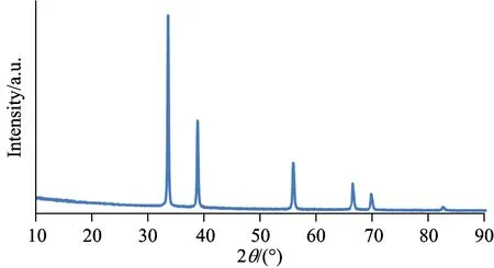
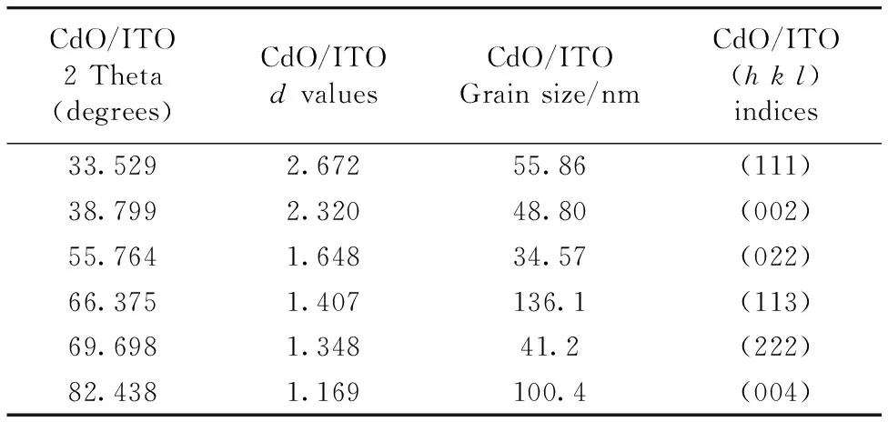
In figure 2, It is seen that XRD spectrum of CdO nanostructures synthesized at room temperature for 3 days. According to Fig.1, CdO peaks which are in accordance with nanocrystal cubic structure peaks. Highest peak comes from (111) crystal plane. Particle sizes for cubic structure peaks, crystal plains on which peaks are obtained and d values are given in Table 1.

Fig.2 XRD spectrum of CdO film
Table 1dvalues, 2 theta (degrees), Grain Size (D) andhklindices of sample

CdO/ITO2Theta(degrees)CdO/ITOdvaluesCdO/ITOGrainsize/nmCdO/ITO(hkl)indices33.5292.67255.86(111)38.7992.32048.80(002)55.7641.64834.57(022)66.3751.407136.1(113)69.6981.34841.2(222)82.4381.169100.4(004)
In Figure 3, SEM microphotographs of CdO films are shown. SEM photos were magnified by 8 000 and 16 000. According to Fig.3, plate (sheet) like nanostructures were observed on the substrate. The layered structures were observed to be nanolayer as seen in Fig.3 and demonstrated a very intensive distribution. This structure can be seen through all surface and homogenous distribution due to crystal structure of ITO. EDS spectrum of this structure can be seen in Figure 4. In the nanostructure, the atomic ratio of Cd∶O is 0.96. This value is very close to 1 and it is a proof that the film formed on ITO crystallizes very good in cubic structure.

Fig.3 SEM microphotographs (8 000 and 16 000 magnifications) of CdO film

Fig.4 EDS spectrum of CdO film
In Figure 5, UV spectrum-Energy band diagram of the CdO nanostructures on ITO substrate. As seen in the absorbtion graph according to wavelength, maximum permeability corresponding to minimum absorption point can be claculated by Beer’s Law equation
(1)
The nanostructure demonstrates extreme absorbtion. The % transmittance amount is extremely low. This shows that thickness of CdO film is highest and is not transmittance.
Energy band diagram of CdO film obtained by using UV spectrum. The energy band gap of bulk CdO was around 2.3 eV but the energy band gap of CdO nanostructure was calculated to be over 3~3.5 eV[3,8-9]. In our study the band gap was calculated as 4.05 eV. This difference about bang gap is due to Burstein - Moss effects in the semiconductors[10].

Fig.5 UV spectrum (a) and Energy Band diagram (b) of CdO film
3 Conclusions
In this study, structural and optical properties of cadmium oxide films deposited by chemical bath technique on ITO substrate were evaluated. The structure formed on ITO crystallized CdO peaks with cubic structures can be observed in XRD spectrum. This structure is compliant to the peaks of CdO nanocrystal cubic structures. Maximum peak was obtained from (111) plane compliant to cubic structure.
In Table 1. the particle size varies between 34 and 136 nm. The average particle size is around 60~65 nm. When the SEM displays of this structure are observed, the structure formed on ITO deposited layer by layer. As the thickness of these layered structures are very low, they are defined as nanolayer or nanoplate. The stochiometric atomic ratio of 0.96 is another proof that this structure demonstrates a very good crystalization on ITO substrate. According to the UV results of this structure, transmittance is very low and absorbtion is high.
In this study when all results were evaluated it was concluded that cubic CdO nanostructures were synthesized succesfully on ITO substrates and the nanostructures had better crystal and surface structure. CdO nanostructures with higher energy band gap compared to bulk structure were obtained. The UV results of the nanostructures with high absorbtion coefficient were observed to be in accordance with the CdO nanoparticles used to examine the antibacterial effect of some bacteria in nanobiotechnology[12]. On the other hand some studies in recent years, It is reported that CdO nanostructures which have cubic crystal structure and such surface properties used in LPG gas sensors[2].
[1] Santos-Cruz J, Torres-Delgado G, Castanedo-Perez R, et al. Thin Solid Films, 2007, 515: 5381.
[2] Bulakhe R N, Lokhande C D. Sensors and Actuators B: Chemical, 2014, 200: 245.
[3] Moumita Ghosh, Rao C N R. Chemical Physics Letters, 2004, 393: 493.
[4] Kamble A S, Pawar R C, Tarwal N L, et al. Materials Letters, 2011, 65: 1488.
[5] Dhawale D S, More A M, Latthe S S, et al. Applied Surface Science,2008,254: 3269.
[6] Perumal P, Gowri Manohari A, Santiyagu Valanarasu, et al. Journal of Surface Engineered Materials and Advanced Technology, 2012, 2: 71.
[7] Baykul M C, Orhan N. Solid-State Electronics, 2014, 101: 29.
[8] Dong Wenting, Zhu Congshan. Optical Materials, 2003, 22: 227.
[9] Moumita Ghosh, Rao C N R. Chemical Physics Letters, 2004, 393: 493.
[10] Ramin Yousefi, Farid Jamali-Sheini, A Khorsand Zak, et al. Ceramics International, 2012, 38: 6295.
[11] Ghatak S, Chakraborty G, Sinha M, et al. Meikap, 2011,406: 3261.
[12] Bahareh Salehi, Sedigheh Mehrabian,Mehdi Ahmadi. 2014,doi:10.1186/s12951-014-0026-8.
Sibel Morkoç Karadeniz1*, Tuba Klnç1, Burcu Bozkurt Çrak2, Tuba Irmaklu1,ÇÇ
1. Department of Physics, Art & Sciences Faculty, Erzincan University, 24100 Erzincan, Turkey 2. Department of Alternative Energy Sources, Vocational School, Erzincan University, 24000 Erzincan, Turkey 3. Department of Electrical and Electronics Engineering, Atatürk University, 25040 Erzurum, Turkey
O657.3
A
10.3964/j.issn.1000-0593(2016)06-1998-03
Received: 2015-10-08; accepted: 2016-02-01
*Corresponding author e-mail: morkocsibel@gmail.com
