Novel dipole UHF RFID tag antenna design
2016-07-04LUOJuYUANQuan
LUO Ju, YUAN Quan
(Chongqing Information Technology Designing Co. Ltd., Chongqing 401121, P.R.China)
Novel dipole UHF RFID tag antenna design
LUO Ju, YUAN Quan
(Chongqing Information Technology Designing Co. Ltd., Chongqing 401121, P.R.China)
Abstract:In order to reduce the size of the antenna and increase the impedance bandwidth, this paper designs a UHF RFID tag antenna, which is based on the large coplanar dipole antenna embedding an asymmetric gap. The antenna size is 70 mm×40 mm×1.6 mm and when S11<-15 dB, the bandwidth is 776-991 MHz.
Keywords:tag antenna; dipole; slot antenna;miniaturization
1Introduction
RFID is an emerging technology used in various fields such as logistics, supply chain and access control[1]. RFID system consists of tags, readers and the host middle ware components. A typical RFID tag consists of an antenna and a chip. Tag antenna and its chips often have complex impedance. Generally the imaginary part of the chip is negative and the value of the imaginary part is usually larger than the real part[2].
In the RFID tag antenna design, it is the one of the most important factors determining the RFID tag antenna system performance. Therefore, this is the researchers and designers of the antenna’s goal, designing an appropriate antenna type of impedance matching with the chip. The label should be small in size, simple structure, low cost and easy to combine with other objects. However, its miniaturized influence radiation efficiency and gain. The maximum of read range between reader and tag will also be affected. Therefore, the size and compromise between the performance of the tag antenna is necessary. To ensure maximum power transmission between the antenna and the chip, we have to ensure good impedance matching.
Currently, some labels antenna are dipole-alike antenna such as bending dipole antenna, folded dipole, helical antenna. Despite the structure is different, their performance is similar to a dipole antenna. Generally, the method modifying the structure of the dipole is often used to reduce the size of the antenna. Curve antenna, spiral antenna and folded dipole antennas are often used to reduce the size. However, the bandwidth of these tag antennas is not enough wide and only can cover an area of UHF RFID. In addition, they are not sufficiently small size[3].In the literature of[3], their dimensions of the proposed two bent dipole antenna are respectively 76.5×16 mm2and 48.5×25.5 mm2and the bandwidth is 860-938 MHz and 901-929 MHz in S11<-10 dB.
The advantages of slot antenna is low profile, low cost and easy to conformal with other objects. Besides, it is easy to combine with active circuits and suitable for mass production, it is very appropriate for application in the RFID[4]. In the paper of[5], a new type of broadband tag antenna was proposed ,covering the entire UHF band. The H-shaped slot is cut on the H-shaped patch.to design a dipole slot antenna. When the antenna is at S11<-15 dB, the bandwidth is 766-989 MHz. In the reference[6], how to shorten the gap size was studied and the symmetric slot antenna is proposed. In addition, the variation of impedance of the antenna with the asymmetric gap was studied. In the literature[3,7-8], other several types of UHF RFID applied to tag antenna system are proposed. Recently, slot antennas in some literature are studied, but only limited to achieve good results in terms of impedance matching. Having not made significant improvements in terms of radiation.
Based on the above research, this paper presents a large coplanar of slot dipole antenna, which open unequal triangular gap on both the size of the square patch and a bottom patch symmetry end cut two corners in order to expand the bandwidth of the antenna.
2Design principles of tag antenna
In the RFID system composed of passive tag antenna, the tag antenna can be divided into two operating modes according to the operating frequency band. The one is suitable for near-field inductive coupling mode, mainly used in low and high frequencies. The another one is suitable for backscatter mode in the far field, mainly used in UHF and microwave bands. Tag is made of the tag antenna and chips .In the process of antenna design, the specific circuit chip needn’t to understand and just need to know the impedance of the chip and design the input impedance of antenna according to the maximum energy transfer rules.
Taking miniaturization and cost into considerations, an additional matching circuit can not be used in the tag antenna design process[9]. In order to achieve maximum energy transfer, the impedance of the antenna is directly matched with the impedance of the chip. The output impedance of the tag chip have a reactance component. So the input impedance of the antenna needs to be designed for the conjugate of the chip impedance. Generally, the input impedance of the electronic tag chip isZ=R-jX. In order to obtain the form of the conjugated impedance, the form of electronic tag antenna impedance should beZ=R+jX.
Passive tags can be simplified as a direct electrical connection between the antenna and the chip. It is particularly important to the interface matching, as the equivalent circuit shown in Fig.1[10].
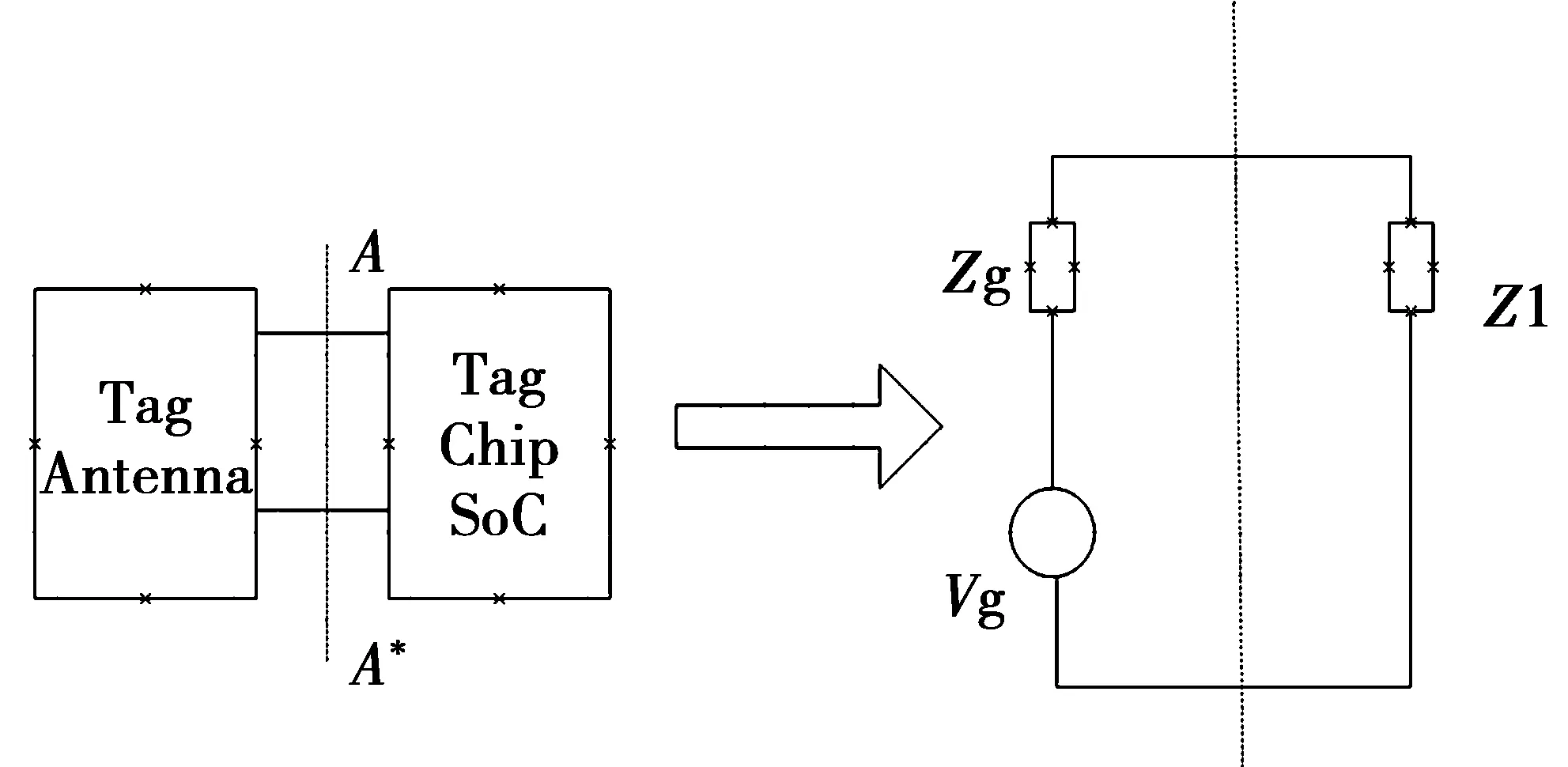
Fig.1 Equivalent diagram of electronic tagmatching principle
As shown in Fig.1, tag antenna is equivalent toZg+vgand tag chip soc is equivalent toZl.
The tag is equivalent impedanceZl. Then load chips obtain the power as follows
(1)
whereZg=Rg+jXG,ZL=RL+jXL.
Seen from the formula, when the impedance of the tag antenna and chip conjugate match, the transmission of chip power is the largest.
Friis equation can be obtained from the tag antenna’s maximum readable distance as follows
(2)
WherePris the received power of the tag(minimum open power);Ptis the transmit power of the reader antenna;Gtis the antenna gain of the reader;Gris the gain of the tag antenna;Ris the distance between the transmitting antenna and the received antenna; andλis wavelength in the vacuum.
If the tag antenna sensitivity isPa,Pa=Pr*τ is the available
(3)
Whereτis in the power transmission coefficient
(4)
Γmis correct reflection coefficient
ZA=RA+jXA,ZL=RL+jXL
(5)

(6)
Whenτ=1 mean an exact match, the identification distance of tag antenna up to the maximum
In the design of the tag antenna, the model of the radiation is also important. In order to have a good read range, a number of RFID applications require some special radiation models, such as omnidirectional or hemispherical coverage[11]. In addition to radiation and the conjugated input impedance model, the shape and miniaturization of this tag antenna is a major factor to consider.
3New design of tag antenna
In this paper, the microstrip antenna based on the original design of the antenna is embedded asymmetrical triangular gap and cut two symmetrical corner in the bottom. With an asymmetric gap increases, the impedance of a slot antenna will get long and in the same gap length conditions, the impedance of the asymmetric slot antenna is more larger than Symmetric slot, easily matched with the tag chip well, while its size can be significantly reduced[6]. Asymmetric triangular groove embedded changes the original path of the surface current on the patch. The triangular seam further increases triangular current path, thereby forming separate current paths, exciting the plurality of resonant mode by adjusting the size and position of each slit, leaving the resonant mode preferably couple and broaden the bandwidth of the antenna. Meanwhile, Asymmetric triangular groove is equivalent to inductance in the circuit such that the antenna presents inductive reactance. Two symmetrical angular cut at the bottom and further increase the inductive of antenna, making the tag chip have a large capacitive impedance which can be better conjugate match.
The novel antenna is a microstrip antenna based on the radiation patch, which made of a dielectric substrate, microstrip feeder, chip. Dielectric substrate using FR4 whose dielectric constant is 4.4, loss tangent 0.02 and thickness 1.6 mm.
Based on the above analysis, the design model of the antenna is shown in Fig.2, and physical graph is shown in Fig.3.
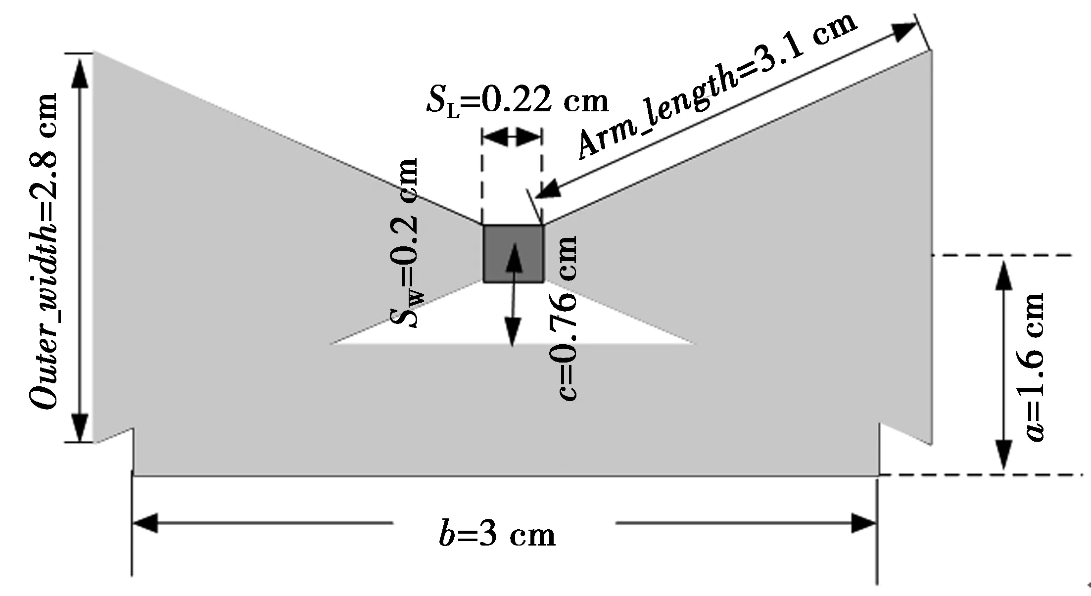
Fig.2 Antenna model
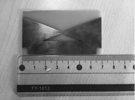
Fig.3 Physical graph
The size of the antenna is as follows:
The length and width of the chip is respectivelySL=0.22 cm,SW=0.2 cm.The length of the edge sides of the slot antenna is 2.8 cm and the larger side of the triangle is 3.35 cm.The height of the medium is 1.6 mm, 40 mm in width and length is 70 mm. The distance from the axis in the end side is 1.92 cm.the bottom side in length is 3 cm.The distance from bottom edges to the center of the rectangular chip is 0.76 cm.
Simulation analysis is carried out on the antenna using simulation software HFSS 13.0, analyzing the influence of several important parameters on the antenna input impedance.
With the arm lengthArm_lengthincreases, the real and imaginary parts of the impedance of the antenna will magnify. WhenArm_lengthis 3.35 cm, the input impedance of the antenna is close to the target impedance .The merit-based selection ofArm_lengthis 3.35 cm. Thus, you can adjust the largest triangular arm lengthArm_lengthand effectively adjust the input impedance of the antenna to get tag antenna impedance matching with the target chip.
First, the analysis is a large triangulararm_lengthof the antenna impacting on input impedance, as shown in Fig.4.
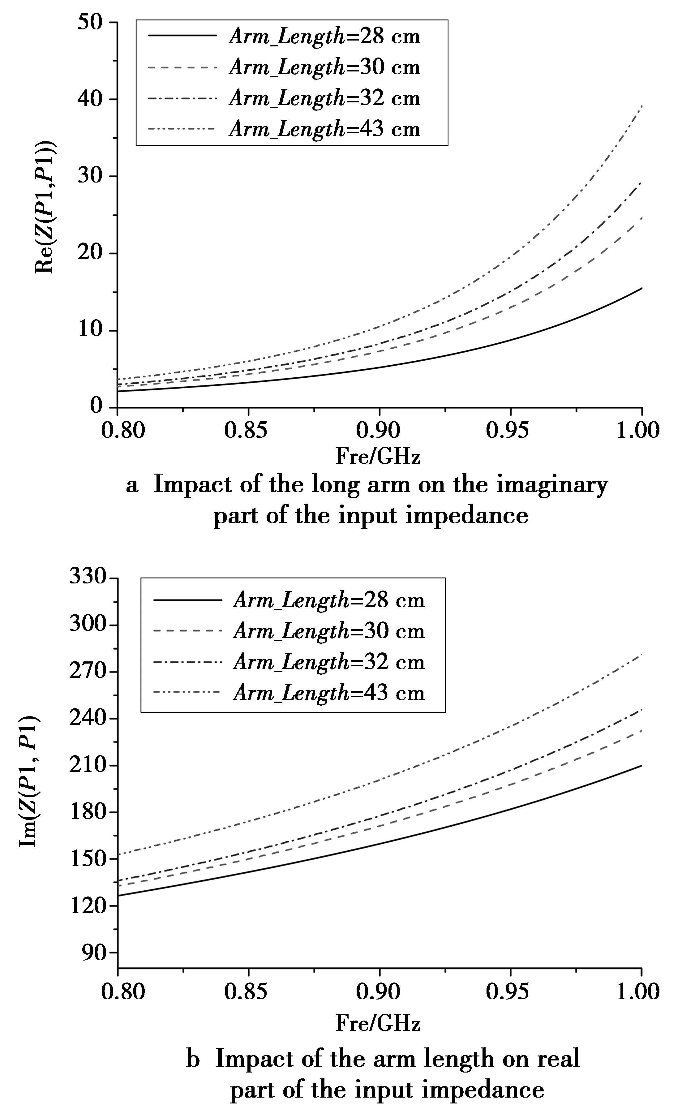
Fig.4 Relationship diagram of antenna parametersArm_Length with antenna input impedance
Then analyzing heightcof the smaller triangles on input impedance of the antenna is as shown in Fig.5.
Fig.5a is the curve of variablecwith the real part of input impedance of antenna changing. The main trend of antenna’s resistance known Fig.5a is ascincreasing will decrease. According to the above analysis, compared with the variableArm_lengthto the impact on the input impedance of the antenna, the impact of the variablecis greater. However, further adjustments of variableArm_lengthcan be considered to the impact on impedance of the antenna. Thus, the value of the antenna parameterscis 0.76 cm.
Based on the above analysis and design, the graph of return lossS11 of the antenna excitation port is shown in Fig.6a. As Fig.6b is shown the simulated results and measured results is basically consistent. In this paper, the tag chip using is ATA5590. The impedance of chip in 915 MHZ is 12-j217. Fig.6 shows that the range of the bandwidth of the antenna is 776-991 MHZ and the bandwidth is 215 MHz

Fig.5 Impact of parameter c on the inputimpedance of the antenna
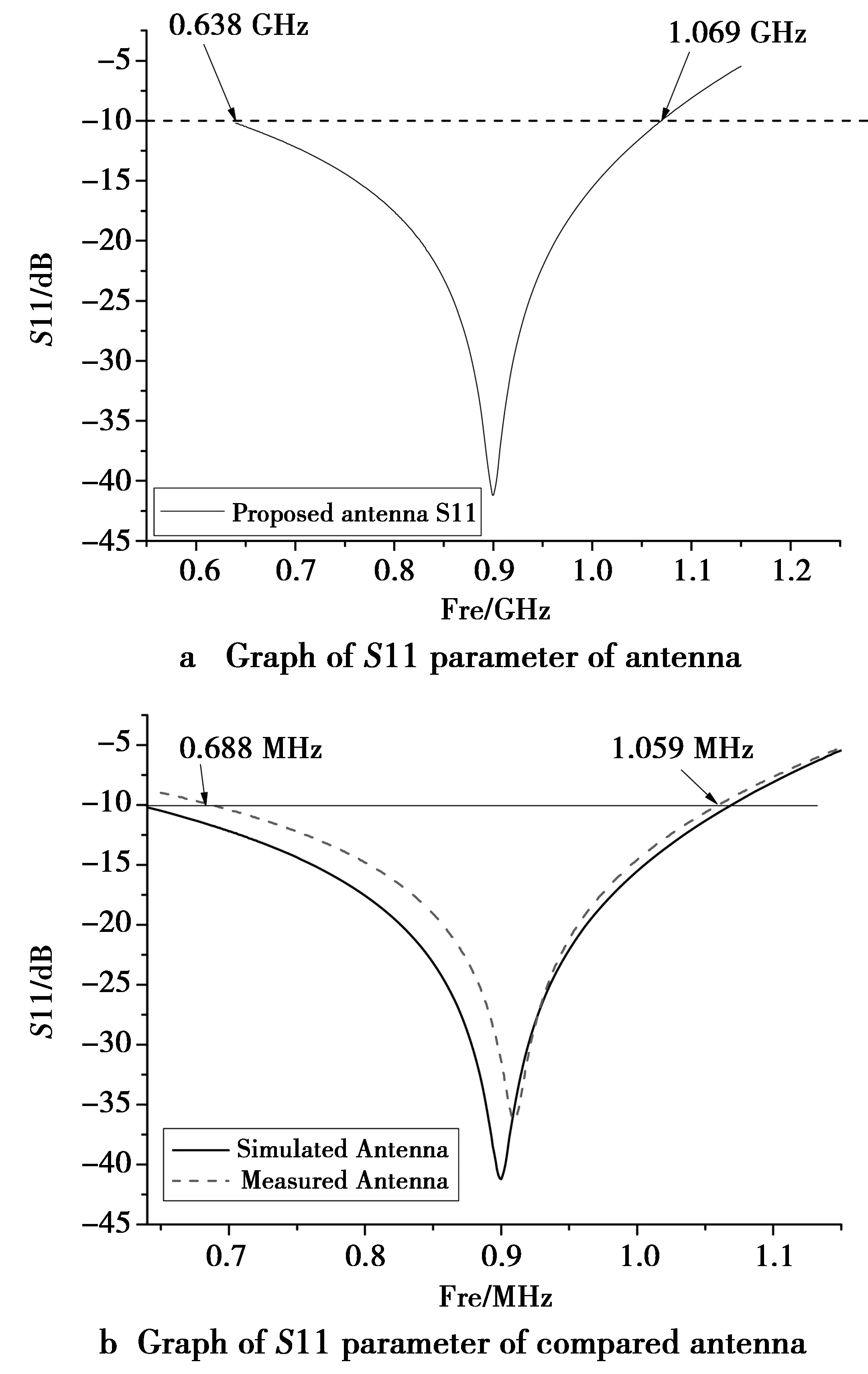
Fig.6 S11 comparison diagram
Fig.4 and Fig.5 are the diagram of input impedance whenArm_lengthis 3.35 cm andcis 0.76 cm. The antenna in Fig.4 and Fig.5 show the input impedance of the antenna isZ=13.53+j210.27 atf=915 MHz, the impedance of the chip 12-j217 ATA5590 conjugate to form a good match.

Fig.7 Gain radiation pattern of the antenna
Fig.7 shows the radiation pattern of the antenna gain has good hemispherical radiation properties, meeting the design requirements.The maximum gain of the antenna is 1.11 dB, having good radiation characteristics.Phiis thexaxis according to counter clockwise around the corner from the positivezaxis.
4Conclusions
In this paper, an asymmetric tag antenna is designed based on a slot antenna. The antenna can achieve good impedance matching by adjusting the size of the gap and the structure is simple and easy to manufacture. Simulation results show that the antenna can cover all bands of UHF RFID system requirements, and relative bandwidth is up to 24.3%.The gain of the antenna reached 1.11 dB, meeting the requirements of the design.
References
[1]PONGPAIBOOL P, WALLADA W, SIWAMOGSATHAM S. A study of multi-conductivity dipole antenna for printed UHF RFID[C]//Consumer Electronics Berlin (ICCE-Berlin), IEEE Third International Conference on. Berlin:IEEE, 2013: 93-97.
[2]ZHOU Y. A novel slot antenna for UHF RFID tag[C]// Wireless, Mobile and Multimedia Networks (ICWMNN 2010), IET 3rd International Conference on. Beijing: IEEE, 2010: 254-257.
[3]HAMANI A, TOUHAMI R, YAGOUB M C E. Novel tag antenna design for UHF RFID applications[C]// 13th Mediterranean Microwave Symposium (MMS). Saida: IEEE, 2013: 1-4.
[4]ZENG W, ZHAO J. A comb-shaped slot RFID tag antenna[C]// Antennas and Propagation Society International Symposium(APSURSI).Toronto,ON:IEEE,2010:1-4.
[5]YANG Hong, ZHENG Yuwei, CHEN Wei, et al. Design of a broadband UHF RFID tag antenna[J]. Electronic components & Materials, 2013, 32(6): 18-21.
[6]ZHOU Yongming, LAI Xiaozheng, LAI Shengli. Design ofRFID tag antenna based on non-symmetrical slot antenna[J]. Journal of Jinan university(Natural Sci & Medicine edition), 2008, 29(5): 466-469.
[7]MA Zhonghua,CHEN Jinxiu, KE youyi. A miniature UHF band circuitous tag antenna[J]. Journal of Fuzhou university(Natural Science Edition),2013(2):182-185.
[8]UKKONEN L, SCHAFFRATH M, ENGELS D W, et al. Operability of folded microstrip patch-type tag antenna in the UHF RFID bands within 865-928 MHz[J]. Antennas and Wireless Propagation Letters, IEEE, 2006, 5(1): 414-417.
[9]KIMOUCHE H, HAMADACHE Z, ATROUZ B. New dipole slot antenna design for RFID communications[C]// Antennas and Propagation (EuCAP), 2010 Proceedings of the Fourth European Conference on. Barcelona, Spain: IEEE, 2010: 1-4.
[10] TANG tao, XIA yunqiang, SONG kaijun, et al. Adjustable impedance matching network for RFID tag antenna test[J]. Chinese Journal of Radio Science, 2013, 28(2): 385-390.
[11] CHEN J P, HSU P. A compact strip dipole coupled split-ring resonator antenna for RFID tags[J]. Antennas and Propagation, IEEE Transactions on, 2013, 61(11): 5372-5376.
Biographies:

LUO Ju(1974-), female, Chongqing, engineer, being engaged in communication and information network research, electronic information research. E-mail: 13883005460@126.com.

YUAN Quan(1976-),male, Suining county, Hunan Province, master, senior engineer, being engaged in wireless communication network research.
(编辑:魏琴芳)
新型偶极超高射频标签天线设计
罗菊,袁泉
(重庆信科设计有限公司,重庆 401121)
摘要:为了减小天线的尺寸,增加阻抗带宽,采用在大共面偶极子天线上嵌入非对称缝隙的方式,设计一款UHF RFID标签天线,实现了标签天线的小型化和宽带化。天线的尺寸为70 mm×40 mm×1.6 mm,S11<-15 dB时,带宽为776-991 MHz。
关键词:标签天线;偶极子;缝隙天线;小型化
DOI:10.3979/j.issn.1673-825X.2016.03.015
收稿日期:2015-06-21修订日期:2016-03-22通讯作者:罗菊13883005460@126.com
基金项目:国家新一代宽带无线移动通信网科技重大专项(2010ZX03001-002-2) The Country’s Major Special Fund of a New Generation of Broadband Mobile Communication Network Science and Technology(2010ZX03001-002-2)
CLC number:TN 821
Document code:AArticle ID:1673-825X(2016)03-0372-05