气压对PLD法在AlN/Si上外延生长的GaN性能的影响*
2016-05-10朱运农王文樑杨为家王海燕李国强
朱运农,王文樑,杨为家,王海燕,李国强,2
1.华南理工大学发光材料与器件国家重点实验室,广东 广州 510640;
2.华南理工大学广东省半导体照明与信息化工程技术研究中心,广东 广州 510640
气压对PLD法在AlN/Si上外延生长的GaN性能的影响*
朱运农1,王文樑1,杨为家1,王海燕1,李国强1,2
1.华南理工大学发光材料与器件国家重点实验室,广东 广州 510640;
2.华南理工大学广东省半导体照明与信息化工程技术研究中心,广东 广州 510640
摘要:采用脉冲激光沉积(PLD)技术在AlN/Si异质结上外延生长GaN薄膜.研究了气压对GaN薄膜结构性能和表面形貌的影响,利用高分辨X射线衍射仪(HRXRD)、原子力显微镜(AFM)和扫描电子显微镜(SEM)对GaN薄膜的结构性能及表面形貌等进行表征和分析.结果表明:气压在1~50 mTorr范围时,GaN薄膜的表面形貌及结构性能均是先好后差;当气压在最佳值10 mTorr时,外延生长的GaN薄膜质量最优,其(0002)和2)面的高分辨X射线衍射摇摆曲线峰值半高宽(FWHM)分别为0.7°和0.8°;原子力显微镜测试得到GaN薄膜表面的粗糙度为1.8 nm.
关键词:气压;脉冲激光沉积;GaN
GaN及其相关的氮化物具有其独特的优势,已经被广泛的应用于制备GaN基LED器件中[1-4].目前商业化LED的衬底材料是以蓝宝石衬底GaN基材料为主,然而蓝宝石价格较高,难以制备大尺寸LED器件,且其热导率低(25 W/Km)、与GaN间晶格失配大(13.3%)及热失配大(27%),不利于大功率LED器件的发展.相比较下,Si衬底具有成本低、质量高、热导率高等优点,有望制备出大功率、大尺寸的LED器件[3, 5-7].但是Si衬底上GaN薄膜异质外延存在一些问题,一方面Si衬底与GaN之间存在较大晶格失配(16.9%)和热失配(-115%),外延得到的GaN材料存在较高的位错密度[7-8];另一方面由于Si和Ga之间的剧烈反应,很难直接生长GaN薄膜[7].而AlN既可以避免SixNy非晶薄膜的形成,又与GaN晶格常数相近,是良好的缓冲层材料.目前,通常采用金属有机化学气相沉积法(MOCVD)在Si衬底上外延生长GaN薄膜[9-11],但这需要较高的生长温度,而且能耗大.此外,采用MOCVD法外延生长III族氮化物薄膜过程中,由于氮源中的N与衬底中的Si发生界面反应,在缓冲层和Si衬底之间形成SiNx,不利于GaN的形核[12-13].为了克服这个问题,采用脉冲激光沉积法(PLD),该法可以提供高能量及帮助表面粒子迁移,使薄膜在低温下生长,这样不仅有效地抑制了薄膜和衬底之间的界面反应,而且降低了能耗[14-16].目前,许多研究者对采用PLD法在Si衬底外延生长GaN薄膜进行了研究,研究主要集中在温度、激光能量等因素对GaN膜质量的影响[17-19],而气压作为一种影响GaN膜性能的关键因素还未被深入研究.
本文采用脉冲激光沉积技术在AlN/Si异质结上外延生长GaN薄膜,并研究了气压对薄膜性能的影响,为制备高质量的GaN薄膜提供工艺参考,对GaN基器件的制备有很大的意义.
1实验部分
采用脉冲激光沉积法(PLD),在5 cm的 Si(111)衬底上外延生长GaN薄膜.激光光源采用波长248 nm的KrF气体准分子激光,以固体AlN(纯度99.99%)和液体Ga为靶材(纯度为99.99999%),N2(纯度99.99999%)作为载气被通入生长室内以保证化学计量的薄膜沉积所需的压力和氮源.
首先将Si衬底先后分别置于H2SO4:H2O2:H2O=3:1:1的混合溶液和5%的HF溶液中,以去除表面污染物和二氧化硅,随后将Si衬底转移至涡轮分子泵控制的压力为6.0×10⁻¹⁰Torr的PLD超高真空生长腔内.在生长之前,首先将衬底在850 ℃下退火60 min,以除去Si衬底表面的残余污染物.先生长30 nm的AlN缓冲层,在Si/AlN异质结外延后,靶材和衬底的距离由80 mm变为50 mm.在GaN外延生长过程中,生长温度为750 ℃,高纯N2通过惰性气体净化器供给,其气压分别为1,10,30和50 mTorr,射频等离子体输出功率为500 W,准分子KrF激光 (λ=248 nm,τ=20 ns) 被用来烧蚀烧结的Ga靶材 (纯度为99.99%) ,其能量为300 mJ/cm2,激光频率为30 Hz.
生长得到的GaN薄膜的结构性能采用高分辨X射线衍射仪 ( XRD,Bruker D8,Cu Kα1X射线源λ=0.15406 nm) 进行表征,表面形貌及结构则分别用扫描电子显微镜 (SEM,Nova Nano SEM 430,荷兰) 和原子力显微镜(AFM,Bruker Dimension Edge,美国)进行观测.
2结果与讨论
2.1气压对GaN薄膜结构性能的影响
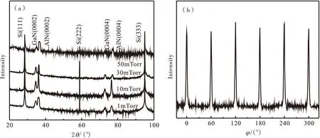
图1 不同气压下外延生长GaN薄膜的X射线衍射图及GaN薄膜2)面的φ扫描图(a)X射线衍射图2θ-ω扫描图;面φ扫描图Fig.1 Typical XRD profiles for GaN films grown on AlN/Si hetero-structures at various nitrogen pressures and XRD φ scans for 2)(a)typical xrd 2θ-ω scan profiles;


图2 GaN外延薄膜的(0002)和2)面的摇摆曲线峰值半高宽数值(a)气压10 mTorr下(0002)面;(b)气压10 mTorr下面;(c)不同生长气压下(0002)和面Fig.2 FWHMs of GaN (0002) and GaN 2) for GaN films grown on AlN/Si hetero-structures(a)X-ray rocking curve of GaN (0002) at 10 mTorr;(b) X-ray rocking curve of GaN 2) at 10 mTorr;(c) FWHMs of GaN (0002) and GaN 2) for GaN films grown on AlN/Si hetero-structures at various nitrogen pressures
2.2气压对GaN薄膜表面形貌的影响
图3为不同生长气压下外延生长GaN薄膜的扫描电子显微镜(SEM)图,其中衬底温度为750 ℃,气压分别为1,10,30和50 mTorr.从图3可以看出:当气压为1 mTorr时,样品表面分布一些团簇的大颗粒;当气压为10 mTorr时,样品表面平整,几乎没有颗粒;当气压增加到30 mTorr时,样品的表面开始出现数个小颗粒;当气压继续增加到50 mTorr,样品表面出现大量的小颗粒.由此可知,气压为10 mTorr时,样品表面最平整.
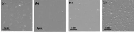
图3 不同生长气压下外延生长的GaN薄膜的扫描电子显微镜(SEM)图 (a)气压为1mTorr;(b)气压为10 mTorr ;(c)气压为30 mTorr;(d)气压为50 mTorrFig. 3 SEM inages for GaN films grown on AlN/Si hetero-structures at various nitrogen pressures (a)1 mTorr;(b)10 mTorr;(c)30 mTorr;(d)50mTorr
图4为衬底温度750 ℃、气压分别为1,10,30和50 mTorr时,外延生长的GaN薄膜的原子力显微镜(AFM)图.从图4中可以看出:气压为1 mTorr时,样品表面存在一些大颗粒,方均根粗糙度(RMS)为7.5 nm;气压为10 mTorr时,样品表面平整,RMS为1.8 nm;气压增加为30 mTorr时,表面出现数个小颗粒,RMS为2.0 nm;气压继续增加为50 mTorr,表面出现大量颗粒,RMS为2.3 nm.由此可知,当气压为10 mTorr时,样品表面粗糙度最小.这是由于气压低时等离子体受到的氮气分子的碰撞比较少,烧蚀粒子相互之间易于聚集形成团簇,在到达Si衬底时会形成凸起的颗粒,同时粒子因为能量比较高,会对已有薄膜产生轰击作用,造成损伤,薄膜表面变得十分粗糙,使RMS的值比较大.而在合适的气压下,等离子体获得适宜的密度和能量,既具有充足的能量进行迁移到平衡位置,又不会对衬底表面和已成核粒子产生损伤,此时RMS值变小.气压较高时,由于等离子体羽辉受氮气分子碰撞的几率增加,极大地减弱了等离子体的能量,于是到达Si衬底的形核粒子密度下降,同时粒子的迁移速度和扩散速度下降,在形核粒子密度很低的情况下,粒子没有足够的能量快速迁移铺满衬底表面,小岛难以合并,导致表面粗糙[24-26].

图4 不同生长气压下外延生长的GaN薄膜的AFM图气压为1mTorr;(b) 气压为10 mTorr;(c) 气压为30 mTorr;(d)气压为50 mTorrFig.4 AFM images for GaN films grownon AlN/Si hetero-structures at various nitrogen pressures(a)1 mTorr;(b)10 mTorr;(c)30 mTorr;(d)50 mTorr
3结论

参考文献:
[1] ZHOU Dong,LU Hai,CHEN Dunjun,et al. Vacuum violet photo-response of AlGaN-based metal-semiconductor-metal photodetectors[J]. Chinese Physics Letters,2013,30(11):117301.
[2] HUANG Kai,GAO Na,WANG Chunzi,et al. Top- and bottom-emission-enhanced electroluminescence of deep-UV light-emitting diodes induced by localised surface plasmons[J]. Scientific Report,2014,4(3):65-65.
[3] YACOUB H,FAHLE D,FINKEN M,et al. The effect of the inversion channel at the AlN/Si interface on the vertical breakdown characteristics of GaN-based devices[J]. Semiconductor Science and Technology,2014, 29(11):115012.
[4] FENGMAO H,YENFU S,KUONING C. Determination of the junction temperature of Gallium Nitride (GaN)-based high power LED under thermal with current loading conditions[C]// Electronic Packaging and iMAPS All Asia Conference (ICEP-IACC).New York:IEEE,2015:691-694.
[5] KROST A,DADGAR A. GaN-based devices on Si[J]. Physica Status Solidi A-Applied Research,2002,194(2):361-375.
[6]YANG Shu,ZHOU Chunhua,JIANG Qimeng,et al. Investigation of buffer traps in AlGaN/GaN-on-Si devices by thermally stimulated current spectroscopy and back-gating measurement[J]. Applied Physics Letters,2014,104(1):013504 (4).
[7] LIN Yunhao,ZHOU Shizhong,WANG Wenliang,et al. Performance improvement of GaN-based light-emitting diodes grown on Si(111) substrates by controlling the reactor pressure for the GaN nucleation layer growth[J]. Journal of Materials Chemistry C,2015,3(7):1484-1490.
[8] AGRAWAL M,RADHAKRISHNAN K,DHARMARASU N,et al. Effect of III/V ratio on the polarity of AlN and GaN layers grown in the metal rich growth regime on Si(111) by plasma assisted molecular beam epitaxy[J]. Japanese Journal of Applied Physics,2015,54(6):065701.
[9] JANG S H,LEE C R.High-quality GaN/Si(111) epitaxial layers grown with various Al0.3Ga0.7N/GaN superlattices as intermediate layer by MOCVD[J]. Journal of Crystal Growth,2003,253(1-4):64-70.
[10] LIU Zhe,WANG Xiaoliang,WANG Junxi,et al. Effects of buffer layers on the stress and morphology of GaN epilayer grown on Si substrate by MOCVD[J]. Journal of Crystal Growth,2007,298:281-283.
[11] WENG X,RAGHAVAN S,ACORD J D,et al. Evolution of threading dislocations in MOCVD-grown GaN films on (111) Si substrates[J]. Journal of Crystal Growth,2007,300(1):217-222.
[12] RADTKE G,COUILLARD M,BOTTON G A,et al. Scanning transmission electron microscopy investigation of the Si(111)/AlN interface grown by metalorganic vapor phase epitaxy[J]. Applied Physics Letters,2010,97(25):251901.
[13] RADTKE,COUILLARD G,BOTTON M,et al. Structure and chemistry of the Si(111)/AlN interface[J]. Applied Physics Letters,2012,100(1): 011910.
[14] CHEN Yuwen,WU Haoyu,YUZhonglin,et al. Post-annealing effects on pulsed laser deposition-grown GaN thin films[J]. Thin Solid Films,2015,577:17-25.
[15]YANG Hui,WANG Wenliang,LIU Zuolian,et al. Epitaxial growth mechanism of pulsed laser deposited AlN films on Si (111) substrates[J]. Crystengcomm,2014,16(15):3148-3154.
[16] WANG Wenliang,YANG Weijia,LIU Zuolian,et al. Achieve 2-inch-diameter homogeneous GaN films on sapphire substrates by pulsed laser deposition[J]. Journal of Materials Science, 2014, 49(9): 3511-3518.
[17] FUJII T,KOBAYASHI A,SHIMOMOTO K,et al. structural characteristics of GaN/InN heterointerfaces fabricated at low temperatures by pulsed laser deposition[J]. Applied Physics Express,2010,3(2):021003.
[18] LI Guoqiang,WANG Wenliang,YANG Weijia,et al. Epitaxial growth of group III-nitride films by pulsed laser deposition and their use in the development of LED devices[J]. Surface Science Reports,2015,70(3): 380-423.
[19] YANG Weijia,WANG Wenliang,LIU Zuolian,et al. Effect of AlN buffer layer thickness on the properties of GaN films grown by pulsed laser deposition[J]. Materials Science in Semiconductor Processing,2015,39:499-505.
[20] WANG Wenliang,YANG Weijia,LIU Zuolian,et al. Synthesis of high-quality AlN films on (La,Sr) (Al,Ta)O3substrates by pulsed laser deposition[J]. Materials Letters,2015,139:483-486.
[21] YANG Hui,Wang Wenliang,Liu Zuolian,et al. Homogeneous epitaxial growth of AIN single-crystalline films on 2 inch-diameter Si (111) substrates by pulsed laser deposition[J]. Crystengcomm,2013,15(36): 7171-7176.
[22] WANG Wenliang,LIU Zuolian,YANGWeijia,et al. Nitridation effect of the alpha-Al2O3substrates on the quality of the GaN films grown by pulsed laser deposition[J]. Rsc Advances,2014,4(75):39651-39656.
[23] WANG Wenliang,YANG Hui ,LI Guoqiang. Growth and characterization of GaN-based LED wafers on La0.3Sr1.7AlTaO6substrates[J]. Journal of Materials Chemistry C,2013(1):4070-4077.
[24] HUANG T F,MARSHALL A,SPRUYTTE S,et al. Optical and structural properties of epitaxial GaN films grown by pulsed laser deposition[J]. Journal of Crystal Growth,1999,200(3-4):362-367.
[25]杨慧.脉冲激光沉积法外延生长大面积AlN单晶薄膜及其生长机理研究[D].广州:华南理工大学,2013.
[26] LOWNDES D H,GEOHEGAN D B,PURETZKY A A,et al. Synthesis of novel thin-film materials by pulsed laser deposition[J]. Science,1996,273 (5277): 898-903.
Effect of nitrogen pressure on the properties of GaN films epitaxially grown on AlN/Si by pulsed laser deposition
ZHU Yunnong1,WANG Wenliang1,YANG Weijia1,WANG Haiyan1,LI Guoqiang1,2
1.StateKeyLaboratoryofLumiescentMetericalsandDevices,SouthChinaUniversityofTechnology,Guangzhou510640,China;2.EngineeringResearchCenteronSolid-StateLightinganditsInformationisationofGuangdongProvince,SouthChinaUniversityofTechnology,Guangzhou510640,China
Abstract:The GaN films have been grown on AlN/Si(111) hetero-structures by pulsed laser deposition (PLD) and the effect of nitrogen pressure on the structural properties and the surface morphologies of GaN films is investigated. High resolution X-ray diffraction (HRXRD), atomic force microscope (AFM) and scanning electron microscope (SEM) are used to characterize and analyze the structural properties and the surface morphologies of GaN films. When the nitrogen pressure changes from 1mTorr to 50 mTorr, the structural properties and the surface morphologies of GaN films are improved at first, and then deteriorated. Meanwhile, it shows an optimum value of 10 mTorr pressure, the as-grown GaN reveals that the full-width at half-maximum (FWHM) of GaN (0002) and 2) is 0.7° and 0.8°, respectively, and very smooth surface with a root-mean square (RMS) surface roughness of 1.8 nm, indicating high-quality GaN films.
Key words:nitrogen pressure;pulsed laser deposition(PLD);GaN
中图分类号:TN304.2
文献标识码:A
文章编号:1673-9981(2016)01-0016-06
作者简介:朱运农(1992-),男,湖北省孝感市人,硕士研究生.
*基金项目:国家优秀青年科学基金(51422203);广东省杰出青年科学基金(S2013050013882);广东省重大科技专项(2014B010119001)资助项目
收稿日期:2015-11-11
