Application of the information encryption technology in the industrial network based on FPGA
2015-10-29YaohuaGUO
Yao-hua GUO
(The Department of Information and Engineering, Tangshan College, Tangshan 063008, China)
Application of the information encryption technology in the industrial network based on FPGA
Yao-hua GUO*
(TheDepartmentofInformationandEngineering,TangshanCollege,Tangshan063008,China)
With the rapid development of information technology industry, information encryption is an effective means of information security. Data encryption system based on FPGA in the field of industry network is elaborated in this paper, and the data acquisition module, the basic principle of 3DES, the implementation in FPGA and PMC bus interface module are introduced. Based on the function simulation, test and analysis of the design results, this scheme shows the characteristics of high reliability, fast algorithm and less hardware resources, and it could be widely used in industrial networks.
FPGA, Data transmission, Encryption technology
1 Introduction
Along with the gradual popularization of computer application in all walks of life and the rapid development of network communication technology, networked data acquisition and transmission system are used in all kinds of data monitoring in the industrial enterprises. In order to assist the managers to make the management and monitoring of data acquired from the field, the RS232/RS485 and various industrial buses are used to form the industrial control network. All data acquired from the field are transmitted remotely to the monitoring centre.Although the widespread use of network monitoring system has realized the automation of industrial production level, the network monitoring bring a lot of conveniences to the enterprise the emergence of network virus and network hacker causes the hidden danger of network data security. How to protect a great deal of data stored and transmitted in the network, especially some important data resources of enterprises, is becoming more and more important so that the data encryption technology is playing an important role in industrial network.
Nowadays, the data encryption technology is mainly used in the field of software, but software encryption can only be treated as software plug-in, and it consumes a lot of CPU time and resources during the runtime. So the demands of speed of system encryption and data transmission were not met, and using the hardware system to realize data encryption work becomes very necessary [1]. A kind of embedded encryption/decryption system is designed in this paper, and the encryption technology is applied for the industrial network, using the high processing ability of Field Programmable Gates Array (FPGA) to realize the 3DES, and making the data transmitted in the network processed by the 3DES encryption, the safety of data transmission is realized without any influence on the transmission efficiency.
2 System design scheme
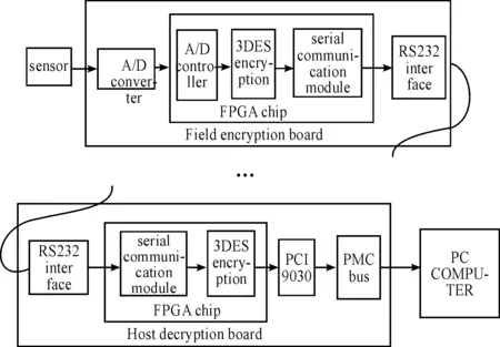
The whole system design scheme is shown in Fig.1. One is the field encryption, the other is the host decryption board. The field encryption board is responsible for the data acquisition and encryption of measured signal in the field. Sensor and control circuit convert the measured signal with 0-5 V (4-20 MA) voltage (current) signal, and transmit it into A/D (ADC0809) converter to realize the analogy-to-digital conversion. The A/D data is transmitted into FPGA for triple data encryption algorithm (3DES) under the control of the FPGA. At last, the encrypted data carry out the long-range data transmission through serial communication interface and coaxial cable. The encryption and decryption function are just opposite.The cryptograph is decrypted by 3DES in the FPGA, and finally transmitted to the host computer through the industry PCI Mezzanine Card (PMC) bus. This process not only guarantees the security of important field data during network transmission, but also will not affect the efficiency of data transmission at the same time. With this encryption and decryption system in the field of industrial control, the data transmitted in the network are all cryptographs. Even if some illegal intruders intercepts data link by some means they will be unable to obtain the plaintext data for no decryption key. So the purpose of transmission security is to protect the confidential data. The normal users establish a secret shared communication channel with the negotiated encryption/decryption key at the time to ensure the security of data. The whole processing system of encryption and decryption is independent of the host, so the high-speed data transmission will not be delayed at the same time. Thus it will not only improve the security of data transmission but also does not consume the host CPU’s processing time.

Fig.1 Diagram of the overall system design
3 System hardware design
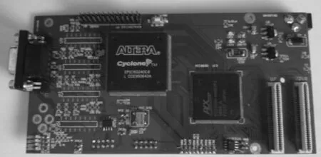
The whole hardware system is composed of encryption card and decryption card. The decryption card is shown in Fig.2.
The whole hardware circuit includes four parts: the A/D converter, the FPGA core chip, serial interface and the host interface hardware module.

Fig.2 Figure of decryption card
3.1 FPGA core chip
As the core of the system, all the data encryption and decryption algorithm are implemented in the FPGA chip, the Cyclone series EP1C60240c8 chips is selected as the FPGA chip. Cyclone series is currently the highest cost-effective FPGA on the market, the chip is based on the process of whole copper 1.5 V SRAM after the cost optimization, with 5980 logical units and as many as 92160 bits embedded RAM, supporting a variety of single-ended I/O standards, such as LVTTL and LVCMOS. There are double data rate (DDR) SDRAM and the interface FCRAM dedicated circuit in the Cyclone chip, and two phase-locked loops (PLLs), providing the hierarchical structure and complex design of clock circuit clock management[2].
The hardware interface card provides the download interface and debugging interface of the FPGA chip design. The download interface is the download hardware description file interface in FPGA. The debugging interface, which is implemented in embedded system, is the interface of embedded processors connections, and this interface typically exists in the high-performance embedded processor.
3.2 Host interface module
The card of Versamodel Eurocard(VME) bus interface in industrial PC is the motherboard and the host decryption card is connected with VME card by PMC bus. Through PMC bus, the decryption data is communicated between card and host PC. So, the decryption card should follow the PMC card design specifications. PMC bus is the Core Memory Core (CMC) card of Peripheral Component Interconnect (PCI) bus defined from two standard forms of IEEE1386 and IEEE1386.1. It is the daughterboard structure of the connection between VME64x board and Compact PCI board.
PCI9030 is a high-performance target interface chip developed by PLX, it could simplify the complex PCI bus control logic into relatively simple local bus control logic, so that the design of the PCI bus interface function can be simplified to the realization of the local bus control logic, and make high-performance PCI bus interface conveniently. The diagram of PCI9030 with PMC bus and FPGA chip connection is shown in Fig.3. The corresponding pins on the PCI side of PCI9030 chip are connected to the corresponding pins of PMC bus, the local bus side is connected with FPGA, PMC bus operations (including reading and writing) can be converted into the operation of local address space by setting the 9030 internal register values to realize data transmission between the FPGA chip and PMC bus.

Fig.3 Diagram of PCI9030 with PMC bus and FPGA chip connection
4 Software module design of FPGA chip
The core functions of encryption/decryption system are all implemented in the FPGA chip. The internal function module mainly includes data acquisition, transmission module, DES module, 3DES module and local bus interface module. Each function module is introduced respectively in details as follows.
4.1 Control of data acquisition and transmission
The A/D converter of data acquisition in the field encryption board is ADC0809. It is a 8-bit A/D converter with 8 channels. The state machine is selected to design the controller of A/D conversion in FPGA. According to the work sequence of ACD0809, the state machine is set to 7 states. The converted 8-bit data form 64-bit plaintext after processing, and then it is transmitted to the 3DES module for encryption.
Universal Asynchronous Receiver/Transmitter(UART) is a kind of universal serial data bus, used for asynchronous communication. The cryptograph data is transmitted through serial communication module in the network, and implement the communication between the field encryption card and the host decryption card. Since the transmitted cryptograph is 64-bit, according to the RS232 serial communication standard, the custom communication protocol is adopted in this process. The total transmitted data is 66 bits which concluds 1 start bit, 64 data and 1 stop bit. Receiving module is carried out in accordance with the definition of 66 bit data frame information.
UART serial communication is mainly divided into three modules: data sending module, data receiving module and the baud rate generator module. Sending module can realize the data delivery and convert form parallel to serial. Receiving module can realize the data reception and the convert from serial to parallel; UART baud rate generator module controls and generates the clock frequency. In order to enhance the anti-interference of data, improve the reliability of data transmission, and also avoid the edge distortion, a “from 1 to 0 jump detector” is designed in the receiving module. When the jump detector receives eight consecutive low at ordinary time, RXD detector will understand that there is a start bit on the RXD and the module comes into the state of receiving data.
A 9600 b/s baud rate is selected in this design, in order to get a precise sampling at the receiving end. Sampling clock frequency is 16 times of the baud rate clock frequency at the receiving end. In the receiving state, receiving controller will sample for 7, 8 and 9 three pulse of data bit, and adhere to the principle of choosing two from three to determine the final receiving value.
4.2 DES principle and FPGA software implementation
Data Encryption Standard (DES) which is belonged to grouping algorithm of symmetric algorithm is commonly used symmetric encryption technology [5]. Because of the high encryption strength, this standard is widely used in many occasions of requiring encryption. In the DES, by combining the technology of confusion and diffusion, which is the substitution first and the replace later, the 64-bit key plays a role in the plaintext and the 64-bit cryptograph is generated after 16 rounds of iterations. It uses the same key during the encryption and decryption process, decryption is an inverse process of encryption. The Fig. 4 shows the whole process of DES. It includes three stages. Firstly, transform the plaintext, take the given 64-bit initial plaintextXas the object, and rearrange theXthrough a replacementIPlist to construct 64-bitX0,XO=IP(X)=L0R0,L0 represents the first 32-bit ofX0,R0 represents the other 32-bit ofX0. Secondly, according to the rules of 16 rounds of iterations to realize the alternation encryption, there are replacements and substitutions during each round [6]. Finally, after 16 iterationIPis used as the inverse displacement. The diagram of each iteration and alternation are shown in Fig.5. The output of each layer alternation acts as the input of the next iteration and the alternation formula of each layer is:
Symbol represents the exclusive or mathematics operation,fis operation function replaced bySbox,Kiis some sub-keys produced by key scheduling function. After 16 rounds of iterations, makeL16R16 replaced inversely by usingIP-1, then get the cryptograph. There are four key points during the process of DES, i.e.,IPreplacement,ffunction, sub-keyKiandSbox.
DES encryption and decryption functions are realized in the FPGA chip. The problem needed to be solved in the design is how to implement 16 rounds of iteration, the maximum efficiency of encryption/decryption, to ensure the implementation speed of the algorithm and to reduce the consumption of the chip resources. In this system, when the plaintext is transmitted into FPGA unit the method of multiple data block assembly line processing is to be used. Firstly, according to the DES grouping method to group the plaintext data, in the first clock cycle, the first block of data after processed in the first round is saved into the register 1. In the second clock cycles, the processed data in the register 1 will be saved into the register 2, at the same time, the second block of data is processed, and the processed data is saved into register 1. In the third clock cycle, the data in register 2 after the third round processing is saved into the register 3, the data in the register 1 is saved into register 2 through the second round of processing, at the same time, a new data after the first round processing is saved into the register 1. So multiple data block assembly line processing can be realized, and the encryption/decryption efficiency could be improved dramatically [7].

Fig.4 Process of DES encryption algorithm

Fig.5 Diagram of 16 rounds of iterations and alternations
4.2.1 IP replacement
Base on theIPlist, theIPreplacement is to recombine the input 64-bit plaintext data and to make the output divided intoL0 andR0 whose length is 32-bit.L0 andR0 are the latter part of rearrangement output.L0 is the left 32-bit of output,R0 is the right 32-bit.L16 andR16 could be achieved after 16 rounds of iterative computations, take these results as the input for inverse replacement, i.e., the result of cryptograph output could be obtained. TheIPinverse replacement is the inverse operation of the initial replacement.
4.2.2 The generation of sub-key Ki
The length of keyKis 64-bit, and the 8-bit, 16-bit, 24-bit, 32-bit, 40-bit, 48-bit and the 64-bit is parity bits, in fact, the real length of key is 56-bit. The values range of the subscript ofKis from 1 to 16, constructed by 16 rounds of iterations. In each round, it applies the bit alteration to choose bit for sub-key, the result of the selection is 56-bit, the first 28-bit is part C and the latter 28-bit is part D. Starting from the first cycle in the FPGA part C and D shift one or two-bit to left during each clock cycle. As the input of next round after latching, after merging by a compression processing, the shifted part C and D produce 48-bit sub-keysK1,K2,K3,…,K16. Using the CASE statement of VHDL language could realize the bit-alteration and compression algorithm during the FPGA implementation.
DES iterative transformation is with 16 rounds, the transformation are selected and shift in each round, after 16 rounds after transformation, a corresponding secret key will be generated in each round. In the hardware implementation of FPGA chip, the design of displacement and compression algorithm is function form. The transformation will call this function in each round, and the corresponding sub secret key is generated ultimately.
4.2.3f function
Theffunction has two inputs, i.e., 32-bitRi-1and 48-bitKi. The 32 bit right parts ofRiis extended to 48 bits through E extend and displacement algorithm. By using the case statement in E algorithm, the 32_bit and some bit from it could make 48-bit data. Finally, the 48 bit output could be obtained through exclusive or operation of the 48-bit input data andKi. The 48-bit will be divided into 8 groups, and each group has six bits and the eighth is the input of the S box.
4.2.4 S box replacement
Sbox that is a complex nonlinear function is a key part of DES algorithm, the design of the box directly affects the whole performance of the algorithm. The main function is to realize the function of the output data of 48 to 32 bits of data conversion. DES has eight box, each box has six input and four output. The conversion from the 48 bit output data to the 32-bit data could be achieved throughS.
In FPGA design of S box , the look-up table (LUT) is used to configurate ROM, the input of the six as ROM address, the ROM corresponding address space store the output of four, thus the six input/output 4 lookup table (LUT) could be realized.
4.3 3DES
Due to the 64-bit length of the key used by DES, the encryption intensity is difficult to meet the requirements. 3DES is a process of data encryption-decryption-encryption, in which the plaintext is encrypted by 3 times. The different keys will be used at each time, and the valid keys are increased to 168 bits. By using 3DES, the encryption intensity will be greatly enhanced, the risk of exhaustion attack in the DES algorithm could be effectively overcome, and at the same time the resistance of linear analysis and the ability of checking are both increased [8]. The diagram of 3DES implementation is shown in Fig.6. The encryption key K1 is used for DES of the plaintext, the key K2 is used for the decryption, the key K3 is also for the encryption, and finally, the cryptograph is output. Triple keys can be the same during the process of 3DES, and also can be different. If the keys are the same, it is the simple DES algorithm, otherwise the 3DES achieves the same strength as 168-bit key and the process of 3DES is the inverse process of the encryption. In the FPGA hardware implementation of 3DES, it uses the design thought of the top-down, and calls DES encryption and decryption module for several times, and finally the 3DES could be realized [9-10].

Fig.6 The diagram of 3DES implementation
4.4 Local bus interface module
Local bus interface module is a module to accomplish the data exchange between the 3DES module in FPGA and local bus. The main operation is the data reading. It could read the plaintext decrypted by 3DES in the latch into the PCI9030 local bus side.
PCI9030 is a PCI-Local Bus bridge interface chip produced by PLX Company. It converts the PCI signal to a Local Bus. Developers don’t need to take care of too much PCI Bus details, only need to operate through the Local Bus, and it can conveniently design module based on PCI Bus. There are many configuration registers in the PCI9030 internal, through operating these registers, the local bus configuration can be carried out, mainly including local address space scope, local space base address registers, and the description registers of the local address space. The address space in the design of size, type, parameters such as the number of address space, can be configured, and different access width and speed can also be set for each address space.
According to the reading, writing and interrupt control sequence of PCI9030 chip, the local read/write operation of interface module could be implemented by state machine. The state transition diagram of local bus is shown in Fig. 7. One time of read (write) operation contains four bus operating state: idle state(idle), address state (address), data/wait state (data/wait) and recovery state (recovery).The data/wait state is divided into write data state and read data state. Local bus adopts the model of reuse, address/data bus for the LAD, address output line address, accept R_sign data line, line including ADSL, LW_RL, RDL, WRL, BLASTL.

Fig.7 The state transition diagram of local bus
5 System test
Select ALTERA corporation Cyclone series EP1C60240c8 chip as the FPGA chip and use VHDL language to design A/D controller, the functions and timing simulations of serial module, 3DES module could be implemented in the QuartusⅡ.
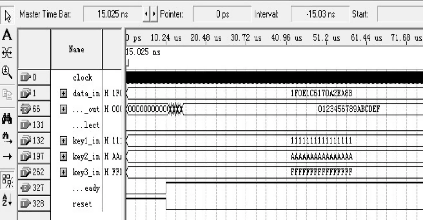
The test results show that the encryption system uses 2024 logic elements (LEs), accounts for 8% of the total 26254 LEs, the decryption system uses 5446 LEs, accounts for 20% of the total Les. It means the hardware resource used by system is relatively few. Fig. 8 is the simulation diagram of encryption system, Key1_in signal is the input of key 1, Key2_in signal is the input of key2, and so on. Function selection signal is the chosen key of encryption and decryption, its high level means encryption and low level means decryption; Data_in signal is the input data of 64-bit plaintext; Reset signal is the reset key; Clock signal is the system clock signal; Data_out signal is the output of the 64-bit cryptograph. The simulation results show that the data_in=(01213456789ABCDEF)H and the password is set as the weak password, Key1_in =(1111111111111111)H,Key2_in=(AAAAAAAAAAAAAAAA)H, Key3_in=(FFFFFFFFFFFFFFFF), and the data_out of the encryption result is 6DCE0DC9006556A3H. Fig. 9 is the simulation diagram of decryption system, the key is the same as encryption and the result of output is (01213456789ABCDEF)H which is the same as input encryption data. Thus, the result verifies the correctness of 3DES encryption/decryption algorithm. It could be concluded that the procedure time of encryption/decryption is only 10 μs per time, and it also verifies the characteristics of high speed of the hardware implementation of 3DES.

Fig.8 The simulation diagram of 3DES encryption

Fig.9 The simulation diagram of 3DES decryption
6 Conclusions
With the development of computer and network technology, the industrial control network in industrial enterprise is applied more and more widely. In order to ensure the safety of the network data transmission, the 3DES is used in the data transmission system. It is implemented with hardware and it makes the encryption intensity higher and the speed faster. Due to the use of custom LAN data transfer protocol, the LAN security and the flexibility of data transmission could be improved.
Application of the 3DES technology based on FPGA makes it true that the industrial control network has a broad and safe prospect. The encryption/decryption system has been designed in this paper, including the field encryption hardware card and the host decryption hardware card. By using the high processing ability of FPGA, the implementation of DES and 3DES in FPGA is designed, and the simulation of the algorithm is accomplished. The hardware implementation of the algorithm obviously improves the speed of the algorithm from the simulation results, its reliability is greatly enhanced. After the encryption algorithm is integrated into industrial control network, the information security of the communication network could be improved. Thus this system can be widely used in the scene of important data encryption or some other scene of needing first-hand information.
Acknowledgements
This paper is supported by Hebei Social Development Research Project(No.13276201D) and Tangshan College Key Laboratory College-level Topic Funded Project(No.140080309).
[1]Liu B F, Zhang H, Wang Y. Application of the encryption technology based on DSP in industry[J].Application of Electronic Technique, 2008, 3: 130-132.
[2]Liu Z W, Tang L C. Design and implementation of security network adapter based on SOPC[J].Computer Engineering, 2006, 34(7): 246-248.
[3]PCI9030 Data book version 1.4[M]. PLX Inc., 2002(5).
[4]Li Q, Wang X G, Li H Z. An implementation of FPGA security based on 3- DES algorithm[J]. Application of Electronic Technique, 2008(1): 132-134.
[5]Yao J, Liu J H, Fan J L. FPGA implementation of DES encryption arithmetic with dynamic key management[J]. Application of Electronic Technique, 2009(7): 145-148.
[6]Chen Y, Wei X, Zhong W. Application of DES encryption algorithm based on FPGA to optical transmission equipment[J]. Optical Communication Technology, 2012(10): 47-49.
[7]Wang L, Wang Y R. Design of reconfigurable system of DES and tri-DES[J]. Computer Measurement&Control, 2009, 17: 751-753,772.
[8]Zhao Y C. The design and implement of 3DES in CA system [D]. Shanghai: FuDan University, 31-38.
[9]Xia S H. DES and RSA encryption algorithm based on the data security transmission technology research[J].Manufacturing Automation, 2011, 33(1): 180-182.
[10]Xue S W. Hardware design of secured module of network interface[D]. Xi’an: Xidian University, 25-27.
10.3969/j.issn.1001-3881.2015.24.016 Document code: A
U285.49
基于FPGA的信息加密技术在工业网络中的应用
郭耀华*
唐山学院信息工程系, 河北 唐山063008
随着工业信息技术的飞速发展,信息加密是信息安全的一种有效手段。阐述了工业领域中基于FPGA的数据加解密系统,介绍了数据采集模块、3DES算法的基本原理及其在FPGA中的实现和PMC总线接口模块。通过对设计结果的功能仿真和测试分析,该方案具有可靠性高、算法实现速度快、硬件资源少的特点,可广泛应用于工业网络中。
FPGA;数据传输;加密技术
22 August 2014; revised 16 April 2015;
Yao-hua GUO, Professor.
E-mail:tdgyh@sina.com
accepted 5 October 2015
Hydromechatronics Engineering
http://jdy.qks.cqut.edu.cn
E-mail: jdygcyw@126.com
猜你喜欢
杂志排行
机床与液压的其它文章
- The design of control system applied in artificial grass tufting machine adopting servomotors
- Research on active suspension control strategy based on fuzzy PID control
- Automobile magnetorheological damper multi-objective optimization analysis
- Co-simulation and consumption analysis of wheel loader on negative loading condition
- Influence of the underlap in the poppet valve on its performance
- Comprehensive reliability evaluation of foreign high-end gantry machining Center
