Efficient Slew-Rate Enhanced Operational Transconductance Amplifier
2015-07-14XiaoPengWanFeiXiangZhangShaoWeiZhenYaJuanHeandPingLuo
Xiao-Peng Wan, Fei-Xiang Zhang, Shao-Wei Zhen, Ya-Juan He, and Ping Luo
1. Introduction
It is well known that the amplifier is the fundamental module in most analog and mixed circuits. And the operational transcondutance amplifier (OTA)[1]is one of the most widely used, which is usually used to drive a capacitive load or a pass transistor in a low dropout regulator (LDR). But due to the limitation of tail current,the driving capability of conventional OTA is weak. And improving the slew rate (SR) is inevitably at the cost of more static power consumption. Today, along with the prevalent use of portable equipment, wireless, and other battery powered systems, the demand for amplifiers with high gain-bandwidth product (GBW), SR, and at the same time very low static power dissipation is growing.
Slew rate enhancement (SRE) techniques have been developed in recent years to solve the problem. Different techniques have been suggested. For example, the dynamic biasing technique[2]-[4]was used to enhance the SR by increasing the bias current of the input differential pair when the differential-mode input voltage was large.Another differential pair was added to sense the input voltage. In [5]-[8], auxiliary branches carried the extra current required by charging/discharging the load during slewing and the core operational amplifier (op amp) would remain unaffected. Both the main amplifier and SRE op amp sensed the same input signal. The SRE amplifier then needed to detect the slewing condition and inject an extra current to the output node. In [9] and [10], the class-AB input stage was used to produce a larger dynamic output current compared with a common differential input pair.
In this paper, a SR enhancement structure is proposed,which transforms a conventional OTA into an efficient one without the static power dissipation or input capacitance increase. To increase the SR, a sensing resistor in series with the diode connecting the metal oxide semiconductor(MOS) transistors of the current mirror is applied. Unlike the diode configured MOS transistor of which the voltage drop is in proportion to the square root of current, it is a linear relationship between the voltage across the resistor and the current through it. Therefore, the voltage drop across the resistor is converted into an output current containing a term in proportion to the square of the voltage by the single-transistor amplifier in the current mirror. The proposed structure, which will be shown below, leads to the essential SR and GBW improvements.
The paper is organized as follows. Section 2 briefly describes the performance of the conventional OTA and the limitation. The proposed SRE technique with the details of its circuit implementation is brought in Section 3. Section 4 presents the simulation results. The paper is concluded in Section 5.
2. Conventional OTA
The conventional OTA is shown in Fig. 1. The p-channel differential input stage comprised of M3Land M3Rconverts the input voltage into currents. Mirrors consisting of M1L, M2Land M1R, M2Rmirror the currents to the output stage. The current generated by the mirror of M1Land M2Lis then mirrored to the output port via the mirror formed by M4Land M4R. The mirror gain factor, K,indicates the current gain in the mirrors formed by M1L, M2Land M1R, M2Rwith the following relations:

where subscripts 1 and 2 indicate that the parameters are corresponding to M1Lor M1Rand M2Lor M2R, respectively.And β=μCoxW/L, where μ is the electron mobility and Coxis the unit-area capacitance of gate oxide, and W/L is the aspect ratio of the MOS transistor.
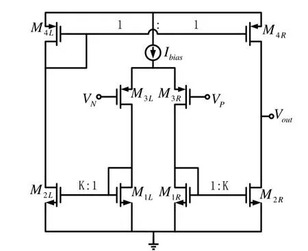
Fig. 1. Conventional OTA.
The conventional OTA is differentiated from other amplifiers by the fact that its only high impedance node is located at the output terminal. The conventional OTA does not employ an output buffer and is, therefore, only capable of driving capacitive loads. The voltage gain of the OTA is given by

where gm3is the transconductance of the differential pair;ro2and ro4are the small signal output resistance of M2Rand M4R, respectively;indicates that ro2and ro4are in parallel. The GBW is given as

where Cloadis the load capacitance and Ibiasis the bias current of the differential pair. Then the SR can be expressed as

It can be seen that for a certain bias current, the GBW and SR increase linearly with the scaling factor K of the current mirror.
The static power dissipation Pstaticis the sum of the product of the power supply voltage with the currents flowing through each branch from the power supply to the ground, which is given by

where Vddis the power supply voltage.
It is obvious that increasing the mirror gain factor K will enhance the SR and GBW at the cost of increasing the static power dissipation. Hence, a trade-off between the driving capability and static power dissipation in the conventional OTA design is required.
3. Proposed SRE OTA
As shown in Fig. 2, the common current mirrors in the conventional OTA are modified by adding two resistors and a bias current sink to each one. This structure reinforces the SR, which will be hereinafter referred to as the SR enhanced structure or SRE mirror.
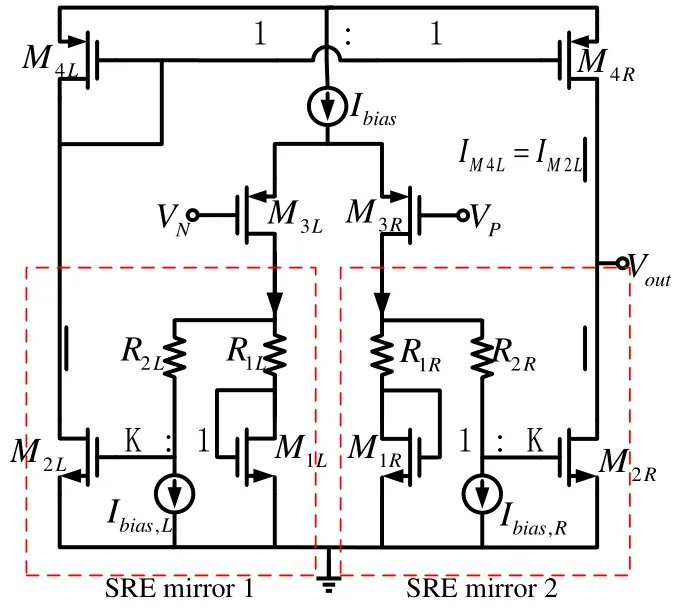
Fig. 2. Proposed SRE operational transconductance amplifier.
In a common current mirror, the output current depends linearly on the input current simply because the non-linearity of the amplifying MOS transistor M2Lis compensated by the non-linearity of the diode-connected MOS transistor M1L. In order to take advantages of the non-linearity of the amplifying MOS transistor M2Lto generate more output current, the non-linearity of the diode-connected MOS transistor must be broken.
Take the SRE enhanced mirror 1 for example. The resistor R1Lin series with the diode-connected MOS transistor M1Lis applied to sense input current and convert it into a voltage including a term linearly depending on the input current. And the output current will include a term containing the square of input current because of the square law characteristic of the amplifying MOS transistor M2L.
The current sink Ibias,Lprovides a constant bias current to R2Land produces a voltage drop across it. Eventually, the static voltage drop across R1Lcan be canceled out by the voltage drop across R2Lwith an appropriate bias current,whereas the dynamic performance will not be affected.
Then, we will analyze the characteristic of the SRE OTA quantitatively. The gate voltage of M2Lis the sum of the voltage across R1Land the drain-to-source voltage of M1Lminus the voltage across R2L, and can be given as

where IM1Lis the current generated from the differential pair minus the bias current Ibias,L. And then, the single-transistor amplifier M2Lconverts the gate voltage into a current which is in a square law relationship with the voltage and is given as

As shown in Fig. 3, the bias current of R2L, which is Ibias,L, is realized by mirroring the tail current. It can be seen that Ibias,L=(m/n)Ibias, where m/n<1/2.
As mentioned before, the bias current of R2Lis properly chosen to set the voltage drop across R2Lto be the same as that across R1Lat the static stage. So, R2L=(n/m-2)R1L/2.Substitute it into (7), the result is

As a result, the relationship between the quiescent current of M2Land M1Lis IM2L,static=K[IM3L-Ibias(m/n)]=KIM1L, just like the common current mirror. But the value of the quiescent output current is[(n-2m)/2n]Ibias, which is less than the common mirror. And by adjusting the value of m/n, the quiescent operating point can be adjusted. Assuming R1L=R2L, m/n=1/4, and βM1L=βM2L, Fig. 4 shows the normalized current transmission characteristic of the SRE mirror with different sensing resistances versus the common mirror. It can be seen the quiescent output current of SRE mirror is half of that of the common mirror. And when R1L=R2L=0, the SRE mirror is similar to the common mirror, so the curve of IM2Lversus IM3Lis linear. When R1L=R2L≠0, the output current increases non-linearly with the input current just as predicted qualitatively before. And the larger R1Lis, the more significant (IM3L-Ibias/2)2term in (8) is. Therefore, the output current increases more quickly with the input current,and exceeds the output current of the common mirror when the input current is over a certain value. And the quiescent operating point has not been affected. Moreover, increasing βM1Land βM2Lsimultaneously, the output current also increases more quickly with the input current, of which the effect is similar to increasing R1L. Decreasing the value of m/n, the quiescent operating point will be moved upwards,and the output current of SRE mirror exceeds that of the common mirror more easily with the increasing of input current, vice versa.
As the positive input voltage Vpis much larger than the negative input voltage Vn, the tail current of the differential pair flows entirely through the transistor M3L. Then (8) can be rewritten as

which is the maximum output current of SRE mirror and also the maximum charging current of the SRE OTA. So the SR can be given as

Obviously, the SR of the SER OTA can be much larger than the conventional one with the same bias current, as long as the values of R1Land βM2Lare large enough and m/n is small (the quiescent operating point moves upwards).Additionally, when the bias current is improved, the SR increases more quickly because of the I2term while the
bias conventional one increases linearly with Ibias.
Then, the static power dissipation of SRE OTA can be expressed as

As can be seen, when m=1/K, the static power dissipation is the same as the conventional one’s for any value of n.
When m>1/K, the static power dissipation is less than the conventional one’s. By increasing m and decreasing n,where n should be larger than 2m, Pstaticdecreases. When m approaches to infinity and n to 2m, Pstaticwill become the minimum value VddIbias(1+K/2).
When m<1/K, the static power dissipation is larger than conventional one’s. Increasing n could decrease the dissipation as much as possible, and the limitation is VddIbias(1+K).
The SR enhanced structure also changes the small signal voltage gain and GBW. The voltage gain is easy to be deduced from small signal analysis and given by

The dominated pole is at the output terminal and given as Pd=1/[(ro2R||ro4R)CL], where ro2Rand ro4Rare the small signal output resistance of M2Rand M4R, respectively.Eventually, GBW is given by

It is obvious that voltage gain and GBW are boosted as well in the SR enhanced structure.
But the added resistors, R1Land R2L, make the internal pole move towards the low-frequency. This degrades the AC small-signal performance. Fig. 5 depicts the AC small-signal model of the part from the drain of M3Lto the gate of M2Lin Fig. 2. The translation function can be given as

where
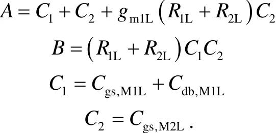

Fig. 5. Small signal analysis of the internal poles and zeros.
It can be seen that this new structure produces two poles and one zero. When the sum of R1Land R2Lare much larger than 1/gm1L, the pole 1/[(R1L+R2L)C2] becomes the most significant one. The high-frequency pole and the zero are very close, which cancels each other’s effect out. So,the structure actually produces one pole 1/(R1L+R2L)C2. If the value of R1L+R2Lis very large, this pole will make the GBW and phase margin (PM) deteriorate. To avoid the deterioration, a compensation resistor is used in series with the load capacitor Cloadto generate a zero 1/RCCloadto cancel the pole out. The resistance of Rccan be given as

4. Simulation Results
A proposed SRE OTA and a conventional OTA are designed with a power supply voltage of 5 V in a 0.5 μm CMOS process to compare their performance. Fig. 6 shows the curves of the unit gain frequency (UGF) and SR versus the resistance of R1L(R1L=R2L=R1R=R2R), and Fig. 7 shows the parameters versus the bias current.
From Fig. 6, it can be seen that the SR of SRE OTA increases with the increase of the resistance as analyzed before. The UGF also increases with the increase of the resistance at first, but tends to be saturated and even decreases when the resistance continues increasing. This can be explained as follows. When the resistance increases,the GBW increases whereas the non-dominant pole, which is the internal pole, moves towards the low-frequency. At first because the resistance is not so large, the internal pole is still at the high-frequency far beyond GBW, which does not affect the UGF. Therefore, the UGF increases with GBW. But when the resistance continues increasing, the internal pole moves towards GBW and even becomes lower than it. So, the effect of the internal pole becomes more significant and makes the UGF be saturated and even decreases.
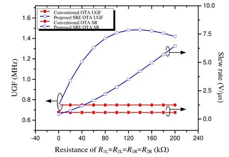
Fig. 6 UGF and SR vs. different resistances R1L=R2L=R1R=R2R(Ibias=5.32 μA, RC=0, Cload=10 pF, m=1, n=4).
From Fig. 7, we can see that the SR of the SRE OTA increases much more quickly with the increase of the bias current than the conventional OTA, because it increases non-linearly with the bias current as analyzed in (10),whereas the SR of conventional OTA increases linearly with the bias current. The UGF of SRE OTA also increases more quickly than the conventional one. The reason is that the transconductance gmof the MOS transistor increases with the bias current as is well-known, and gm2Land gm3Lboth contribute to the increasing of the GBW of the SRE OTA whereas only gm3Lcontributes to the increasing of the conventional one according to (3) and (13).
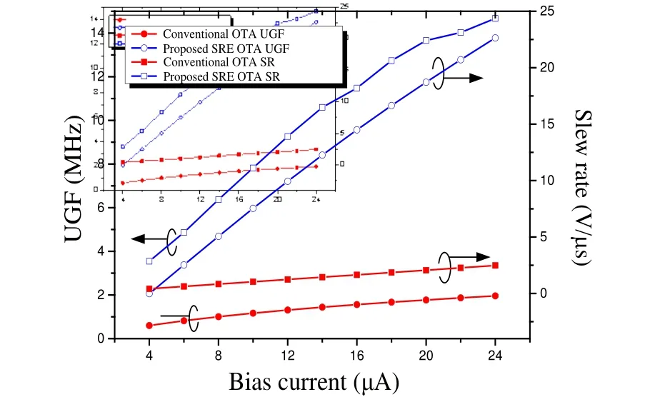
Fig. 7. GBW and SR with different bias currents(R1L=R2L=R1R=R2R=150 kΩ, RC=7 kΩ, Cload=10 pF, m=1, and n=4).
The AC small-signal characteristic is shown in Fig. 8. It can be seen that the low-frequency gain and UGF of the SRE OTA are both higher than those of the conventional one, agreeing with the small signal analysis in Section 3.
The output settling time simulation results are shown in Fig. 9. The output of the SRE OTA settles much faster than the conventional OTA.
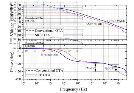
Fig. 8. Frequency response of the SRE OTA and conventional OTA (Ibias=5.32 μA, R1L=R2L=R1R=R2R=150 kΩ, RC=7 kΩ, Cload=10 pF, m=1, and n=4).
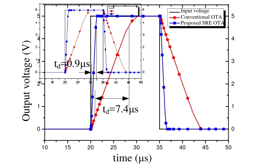
Fig. 9. Output settling time simulation of the SRE OTA and conventional OTA (Ibias=5.32 μA, R1L=R2L=R1R=R2R=150 kΩ,RC=7 kΩ, Cload=10 pF, m=1, and n=4).
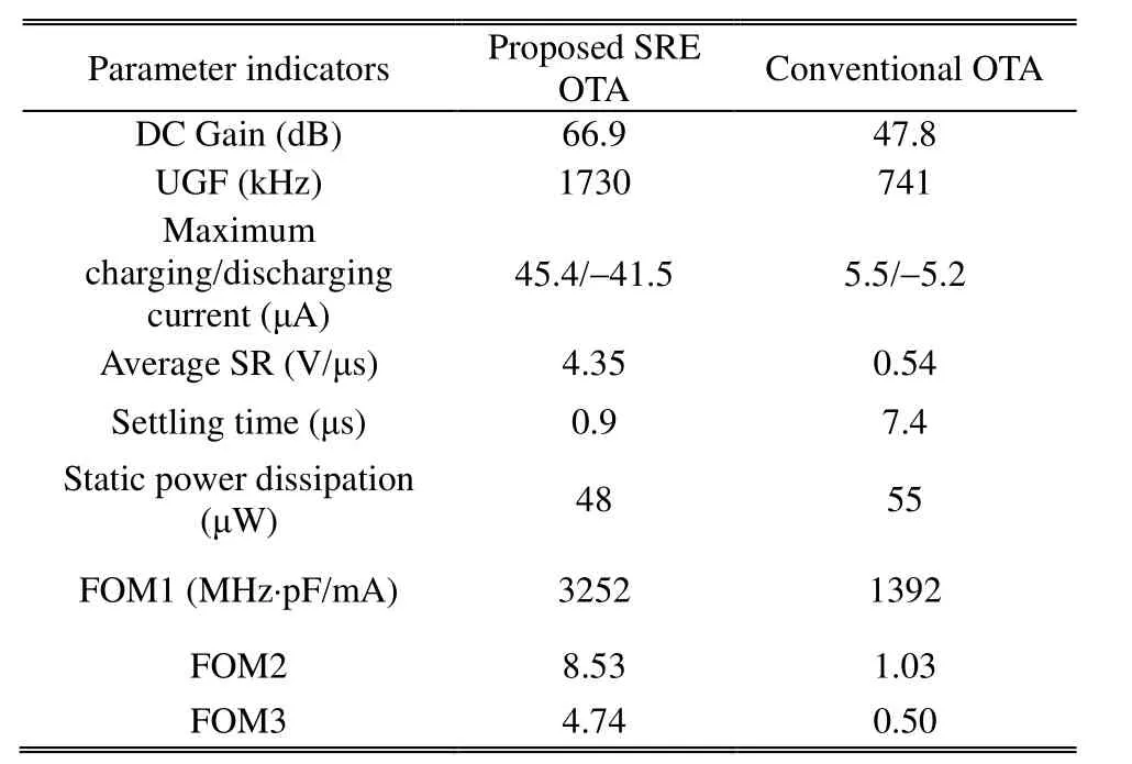
Table 1: Simulation results comparison(Ibias=5.32 μA, R1L=R2L=R1R=R2R=150 kΩ, Rc=7 kΩ, CL=10 pF,m=1, and n=4)
Simulation results are summarized in Table 1. The figures of merit (FOMs) shown in Table 1 are important quality factors reflecting the driving capability and power dissipation of an amplifier. And FOM1[1], FOM2[10], and FOM3[10]are defined as follows:

where ILmaxis the maximum output current provided to the load and Isupplyis the total quiescent current of the supply voltage. In this work, these factors have been greatly improved. FOM1, FOM2, and FOM3 have been improved 134%, 728%, and 848% respectively.
5. Conclusions
In this study, a sensing resistor in series with the diode configured MOS transistor of the current mirror is applied to increase the SR. Therefore, the voltage drop across the resistor produces a term containing the square of the input current in the output current of the SRE current mirror. As a result, the op amp has a greater SR which has been improved by 8.25 times. And at the same time, the UGF is improved by 2.33 times, whereas, the static power dissipation is reduced 12.7%. Compared with some common methods of SR enhancing, this method does not lead to more power dissipation and even reduces it, which is a great merit. Especially for today, the use of portable equipment, wireless, and other battery powered systems are prevalent, improving the driving capacity with no more power dissipation has great significance. But, the SR of this method is still not high enough, and it is necessary to improve it more for further study.
[1] W. M. C. Sansen, Analog Design Essentials; Dordrecht:Springer, 2006, ch. 6.
[2] E. A. Vittoz, “The design of high-performance analog circuits on digital CMOS chips,” IEEE Journal of Solid-State Circuits, vol. 20, no. 3, pp. 657-665, 1985.
[3] G. C. Cardarilli and G. Ferri, “CMOS adaptive biasing circuits for low-power applications,” in Proc. of the 21st Int.Conf. on Microelectronics, 1997, pp. 747–750.
[4] S. Baswa, A. J. Lopez-Martin, R. G. Carvajal, and J.Ramirez-Angulo, “Low-voltage power-efficient adaptive biasing for CMOS amplifiers and buffers,” Electronics Letters, vol. 40, no. 4, pp. 217–219, Feb. 2004.
[5] K. Nagaraj, “CMOS amplifiers incorporating a novel slew rate enhancement technique,” in Proc. of the IEEE 1990 Custom Integrated Circuit Conf., 1990, pp. 11.6.1–11.6.5.
[6] R. Krithivasan, L. Yuan, L. Najafizadeh, Z. Chendong, C.Suheng, C. Ulaganathan, and B. J. Blalock, “A high-slew rate SiGe BiCMOS operational amplifier for operation down to deep cryogenic temperatures,” in Proc. of IEEE 2006 Bipolar/BiCMOS Circuits and Technology Meeting, 2006,pp. 72-75.
[7] H. Lee, P. K. T. Mok, and K. N. Leung, “Design of low-power analog drivers based on slew-rate enhancement circuits for CMOS low-dropout regulators,” IEEE Trans. on Circuits and Systems II, vol. 52, no. 9, pp. 563-567, 2005.
[8] X. Lei, D.-B. Fu, D.-M. Zhu, and C. Su, “A novel high-transconductance operational amplifier with fast setting time,” in Proc. of the 10th IEEE Int. Conf. on Solid-State and Integrated Circuit Technology, 2010, pp. 500–502.
[9] A.-R. Kim, H.-R. Kim, Y.-S. Park, Y.-K. Choi, and B.-S.Kong, “Low-power class-AB CMOS OTA with high slew-rate,” in Proc. of 2009 Int. SoC Design Conf., 2009, pp.313–316.
[10] A. J. López-Martín, S. Baswa, J. Ramirez-Angulo, and R. G.Carvajal, “Low-voltage super class AB CMOS OTA cells with very high slew rate and power efficiency,” IEEE Journal of Solid-State Circuits, vol. 40, no. 5, pp.1068-1077, May 2005.
杂志排行
Journal of Electronic Science and Technology的其它文章
- Non-Supervised Learning for Spread Spectrum Signal Pseudo-Noise Sequence Acquisition
- Face Detection under Complex Background and Illumination
- Transformation of Voltage Mode Filter Circuit Based on Op-Amp to Circuit Based on CCII
- An Evolution, Present, and Future Changes of Cloud Computing Services
- Backlit Keyboard Inspection Using Machine Vision
- Polarization-Dependent Optimization of Fiber-Coupled Terahertz Time-Domain Spectroscopy System
