Light management in crystalline silicon solar cells
2013-11-26DINGWuchang
DING Wu-chang
(Institute of Microelectronics,Chinese Academy of Sciences,Beijing 100029,China)
*Corresponding author,E-mail:huailiang@jlu.edu.cn
1 Introduction
Light management is one of the most critical factors for high efficiency crystalline silicon solar cells,which can directly affect the short-circuit current(Jsc)of the cell.Three types light management methods are most concerned nowadays for improving cell performance:antireflection(AR),light scattering and light-trapping.The main aim of AR technique is to reduce the surface reflection and let more incident light enter into the cell.Light scattering changes the propagation direction of the light to increase its absorption path length,while light-trapping confines the light in the cell via scattering and internal reflection.
As the expected wafer thickness will be reduced to 120 μm in 2020 for crystalline silicon solar cells[1],light management becomes more important to maintain a high Jsc.The light management methods mentioned above may be combined to reach full light utilization.This review presents selected stateof-the-art light management techniques,and the basic principles for the design of the light management structures are summarized and discussed.For clarification,compatible fabrication process should be developed for specific light management structure to fully utilize the beneficial of extra light absorption.For example,silicon nanowire arrays will increase the cell surface area,new surface passivation and electrode formation techniques are required to optimize the performance of the cell[2-3].
2 Antireflection
2.1 Dielectric thin films coating
2.1.1 Basic principles
Dielectric thin films are generally used as AR coatings base on mature and simple fabrication techniques,such as PECVD or magnetic sputtering.Fig.1 illustrates the principle of thin film antireflection where one-layer thin film was used as an example.The thin film creates double interfaces,resulting in two reflected waves.If the relative phase shift is 180°for the two waves,destructive interference occurs,cancelling all the reflected waves partially or completely before they exit the surface.
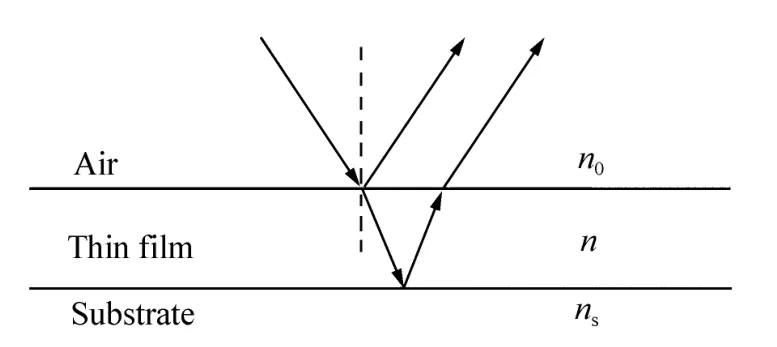
Fig.1 Schematic of AR principle by thin films
Numerical design is an effective way to achieve high efficiency silicon solar cells[4].To design effective dielectric thin film coatings,a convenient theoretical method was developed based on the concept of optical admittance[5].Optical admittance is defined as the ratio of the magnetic and electric fields,y=H/E,which is related to the refractive index of the medium:
where N is the complex refractive index of the medium and У is the optical admittance in free space.Under this definition,multiple thin films could be replaced by a single surface with an admittance Y,which is the ratio of the total tangential magnetic and electric filed and is given by
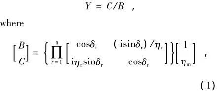
δr=2πNdcosθ/λ is the phase variation of the light in the thin film,ηris the optical admittance of the rthlayer thin film counted from the air and ηmis the substrate admittance. Reflectance, transmittance and absorbance of thin film coatings could be con-veniently obtained by,
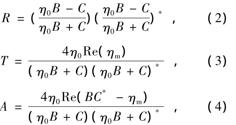
where η0is the optical admittance of the air.
For completely extinction of surface reflection at a certain wavelength λ,single layer dielectric thin film should fulfill the following requirements.Firstly,the refractive index of the thin film should be n,where nsand n0are the refractive index of the substrate and the incident medium.Secondly,the optical thickness of the thin film should be odd numbers of quarter wavelengths(λ/4).Silicon nitride approximately meets these requirements for silicon substrate.And due to its compatible deposition technique with crystalline silicon solar cells,it is widely used in industrial solar cells production nowadays.However,the exactly cancellation of the reflection via single layer dielectric coating is only valid for a specific wavelength.For a wavelength offset,the antireflection effect will be degraded dramatically.
For silicon solar cell application,the reflectance should be minimized in a wide range of wavelength,particularly under AM1.5 spectra.Multilayer thin films coatings or surface texture techniques have been investigated for this purpose.To evaluate the effectiveness of these AR structures,average reflectance under AM1.5 spectra is proposed as,
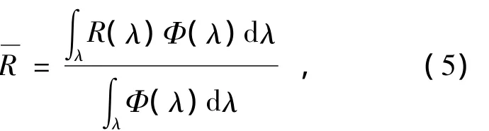
where R(λ)is the reflectance varied with incident wavelength,and Φ (λ)is the incident spectra.Sometimes response of the silicon solar cell is also considered for more accurate evaluation,which results in:

where C(λ)is the internal quantum efficiency of the silicon solar cell.
As discussed above,antireflection design of silicon solar cell usually demands a minimized total reflectance.However,sometimes the absorption of the dielectric thin films is also very important for the optimization of silicon solar cell absorption,such as TCO or silicon rich silicon nitride with a non-zero optical extinction coefficient.For these cases,maximized transmittance is more suitable for the design of optimized cell absorption[6].And evaluation formula can be easily deduced via substitute R(λ)with T(λ)in equation(5)or(6),where T(λ)is the transmittance of the films.
2.1.2 Multiple dielectric thin film coatings
As mentioned above,silicon nitride thin films are commonly used for silicon solar cells as a singlelayer AR coating.To reach a wide range antireflection,double-or multiple-layer dielectric thin films are required.Graded refractive index configurations are usually adopted to form efficient AR coatings,in which refractive index decreases sequentially from the silicon substrate to the air.As silicon nitride is generally used in silicon solar cells,the silicon-rich nitride(SRN)thin film with high refractive index is considered to construct double layer coatings with silicon dioxide[5].Numerical and experimental results show a relatively low surface reflectance could be achieved compared with single silicon nitride,as shown in Fig.2.The minimum average reflectance is only 1.32%in the wavelength region of 400-1 000 nm.The SRN/SiO2double AR coating is particularly suitable for ploy-crystalline silicon solar cells,for which the surface texture is difficult and multiple thin films are commonly used as anti-reflection structures.However,the SRN thin film must have a relatively high refractive index to reach a minimum surface reflection.Therefore,the extra silicon content is consequently high,and extra absorption loss will occur in SRN film.This will especially affect the short wavelength region.A trade-off between low surface reflection and SRN absorption result in refractive index around 2.2 is adopted in the practical application.
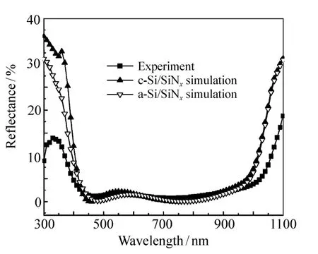
Fig.2 Numerical and experimental reflectances ofSRN/SiO2double AR coatings[6]
SRN thin film can be treated as a mixture of silicon and silicon nitride,in which the absorption due to extra silicon is a total loss mechanism.Silicon nitride covered silicon nanowires is another interesting AR structure based on silicon and silicon nitride,in which the generated carriers in silicon nanowires can be gathered by the p-n junction.This structure can be decomposed as three layer thin film coatings with graded refractive indexes,and its AR properties can be well simulated under transfer matrix calculation[7].Under proper design using optical admittance calculation,this triple-layer antireflection coating can reach rather low surface reflectance,as shown in Fig.3.An average reflectance of 1.3%under AM1.5 spectra in 450 nm to 900 nm range has been achieved with 60 nm silicon nitride coating[8].However,the diameter of the nanowires investigated is around 250 nm in 450 nm pitch,which is difficult for mass production.Novel technique such as low-cost nano imprint should be developed for its practical application.

Fig.3 Antirefleciton characteristics of silicon nitride coated silicon nanowires,where t is the thickness of silicon nitride[8]

Fig.4 Schematic and SEM image of triple AR coating with an ultra low refractive top layer
For thin films with graded refractive index profile,if ultra low refractive index can be obtained for the thin film adjacent to the air,it will be quite beneficial for AR characteristics,which let the incident light enter into the thin films more easily.Sameer Chhajed deposited nano-structured SiO2thin film to achieve an ultra low refractive index around 1.07[9](see Fig.4).And combined with SiO2and TiO2,a triple-layer AR coating was fabricated with improved antireflection characteristics.Except for low reflectance over the whole solar spectrum,low reflectance is also achieved in a wide range of angle of incidence(AOI).An average reflectance of only 5.9%was achieved in wavelength range of 400-750 nm and incident angle range of 40-80°.Compared to single silicon nitride coating with an average reflectance of 17.3%,the surface reflectance is efficiently compressed by the tripe-layer AR coating.
As theoretical calculation predicted,the multiple graded index thin film coatings can perform a near perfect antireflection[10]. Several deposition techniques including the oblique angle deposition was developed to achieve multi-layer thin films with graded index profile experimentally.An example of multiple layer coatings was shown in Fig.5[11].A seven-layer thin film was deposited or co-sputtered on silicon substrate.The bottom two layers are made of TiO2,which have relative high refractive indexes.The middle three layers are mixture of SiO2and TiO2with different compositions.And the top layers are made of porosity SiO2with ultra low refractive indexes of 1.22 and 1.09,respectively.An average reflectance over a wavelength range of 400 nm to 2 000 nm and a incident angle range of 8°to 60°was measured.The graded index thin films achieved an average reflectance of 3.79%which is much lower than the traditional single λ /4 coating(18.8%).

Fig.5 SEM image of a seven-layer AR coating with refractive index denoted,and deduced reflectance under 8°incidence for the AR coating
2.2 Textured surfaces for antireflection
Surface texture is another most common technique to eliminate surface reflection of silicon solar cells.Including pyramids texture which is already generally used in industrial crystalline solar cells,various texture structures have been developed for silicon solar cell application,such as nanowire arrays(NWAs),nanopores(NPs),subwavelength structures(SWS),and other ordered periodic surface textures[12-14].Graded effective refractive indexes of these structures result in ultra low surface reflection.In other hand,scattering effect in texture surfaces also contributes to the AR ability.
2.2.1 Fabrication processes
Metal-assisted chemical etching is a convenient way to fabricate nanostructure surfaces.This method is broadly adopted due to its simplicity,large-scale and low-cost fabrication processes.Many metals like Ag,Au,Pt et al.can be used as an etching medium.Fig.6 gives an example of metal-induced chemical etching process:Ag particles on H-teminated silicon surface are deposited via electroless metal depositoin or thermal evaporation technique.Then the sample was submerged in HF with H2O2oxidant for chemical etching.Various possible cathode and anode reaction processes have been proposed to explain preferential etching at metal/silicon surface.The reaction processes in Fig.7 is one of the well accepted models for Ag-assisted reaction process[15].After the selective etching process,textured surfaces such as nanowire arrays will be formed.Combine with other mask technique,metal-assisted chemical etching can be used for various texture surface fabrications.
Metal-induced growth can also form nanowire arrays in an opposite direction compared with metalassisted chemical etching,which has been well known as Vapor-Liquid-Solid(VLS)method.A thin metal layer is pre-deposited/evaporated on silicon substrate,and then the metal-coated substrate is annealed under vacuum to catalyze the silicon nanowire growth.Silicon nanowires are grown in a chemical vapor deposition reactor with H2diluted pyrolyzing silane as precursors.VLS method has a history of over 50 years,which is very mature for silicon nanowires growth[16].
Nano imprint is a low-cost technique for nanotexture fabrication compared with lithography.In this technique,nano-scale structures are firstly fabricated via lithography technique(or two-beam interference lithography technique)on a flexible master.Then the structures are transferred into UV sensitive resist via rolling press process(Fig.7)[17].Reactive ion etching is finally applied for silicon surface texturing.Though the master fabrication need lithography technique,it can be repeatedly used which is beneficial to mass production.
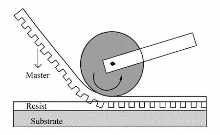
Fig.7 Schematic of nano imprint process[17]
Porous alumina membrane mask is generally used to fabricate subwavelength AR structures.It has been proved that two-step anodizing process can form an ordered mask for silicon substrate etching[18].However,this process consumes very long time,and it is difficult to transfer the alumina mask onto silicon substrate.Thus,a much convenient way is to deposit alumina on silicon and then fabricate the mask in situ.Fig.8 shows an example of surface texturing process with Al2O3mask.500 nm Al was sputtered on silicon substrate with an oxidation surface.Then the Al thin film was electrically oxidized in oxalic acid solution under 40 V contrast voltage to achieve a porous Al2O3mask.Phosphoric acid was used for the pore widening and then fast atom beam etching was performed for silicon surface texture[19].
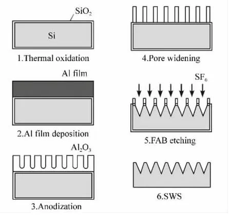
Fig.8 An example of surface texture process via Al2O3 mask technology[19]
Also other techniques have been used for surface texture or patterning,such as laser interference lithography, PS sphere template etching[20-23].Sometimes combined techniques like template metalassisted chemical etching should be employed to form specific texture surfaces[24-26].
2.2.2 Antirefleciton properties of nano-textured surfaces
Textured surfaces include large-scale texture,such as pyramids texture,and small-scale texture,such as nanowires and nanopores.The AR principles for various size textures are quite different.For texture with large scale far surpassing the incident wavelength,the main AR mechanism is multiple reflections between different sides of the texture,which can be easily understood under geometrical optics.But for texture with small scale that can be compared with the incident wavelength,the exact behavior of the light must be predicted under wave optics.Based on Maxwell equations,some numerical methods have been proposed for AR properties calculation and design of these textures,such as RCWA(theRigorousCoupled-WaveAnalysis)method.Furthermore,the Maxwell equations are still undoubtedly suitable for characteristics prediction of surface texture with scale far smaller than the incident wavelength.However,since the texture scale are too small,it seems like a uniform medium from the incident light view.Thus,geometrical optics can also be applied to explain some behaviors of the light.An example has already been mentioned in section 2.1.2 where effective refractive index has been used to evaluate the AR ability of thin film coated nanostructures.
Large-scale texture techniques have already been employed in industrial production.Researchers are now devoted to small-scale texture techniques,especially nano-scale texture techniques,which have more efficient AR abilities.The most common nanotextured surfaces used for silicon solar cell are nanowire arrays(NWAs),nanopores(NPs)and subwavelength structures(SWS).Excellent AR abilities have been proved on all these structures.Here,random or ordered NWAs and moth-eye type SWS structures are selected as identical nano-textured surfaces.
NWAs fabricated via metal-induced etching usually have disordered orientation,though metal particles moves in a preferential direction during the etching process[26-27].Whatever,ultra low surface reflection has been achieved on these disordered NWAs.The reflectance of NWAs after different etching duration is shown in Fig.9[27].After etching for two hours or longer,reflectance below 3%has been achieved in the whole wavelength range of 300-1 000 nm.The excellent AR characteristics of disordered NWAs are benefited from the effective graded refractive indexes and scattering between nanowires. However, the long etching time increased fabrication cost.Fast fabrication process should be further developed for practical application.
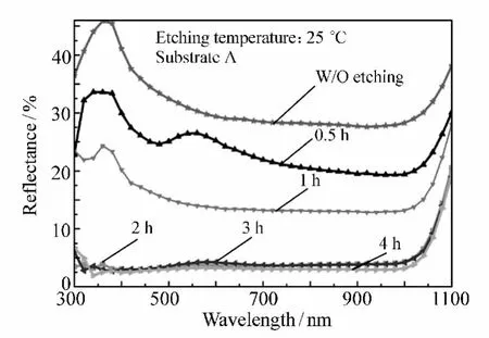
Fig.9 Reflectances of NWAs fabricated via metal-induce etching for different durations[28]
Another example of disordered NWAs was manufactured by VLS method by G.Grzela[29].The NWAs with low filling fractions of 0.02 for vertical and 0.005 for nonvertical nanowires were deposited using gold as the induced grown metal.Thus,the effective refractive index of the NWAs layer is very low which makes the incident light easily enter into the layer.Then,the light is extinct by scattering and absorption.Also,it is proved that the low filling fraction NWAs have excellent anti-reflective abilities in a wide wavelength range and incident angle range,which is quite beneficial to solar cell application.
Antireflection using period/ordered NWAs also has been widely investigated.A convenient way to obtain periodical NWAs is using self-assemble PS sphere or other particles as masks.Crystalline silicon solar cell with an efficiency of 9.24%has been achieved usingperiodicalNWAsasAR structure[21].Due to low surface reflectance as shown in Fig.10, the short-circuit current Jscreaches 29.5 mA/cm2under AM1.5 illumination.
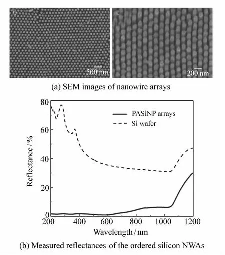
Fig.10 SEM image of nanowire arrays fabricated by PS sphere template RIE etching,and measured reflectances of the ordered silicon NWAs[21]
Towards perfect surface antireflective characteristics,complex nano-strutured surface were explored.The most famous architecture is moth-eye type SWS.Moth-eye structures have a gradually decreased effective refractive index profile from the substrate to the air,resulting in ultra low reflectance in a wide wavelength and incident angle range.Q.Chen fabricated moth-eye type nanopilliars using nanoimprint technique.Ultra-low average reflectance of 1%was achieved in the spectral range of 400-1 000 nm[17].And the average reflectance is still under 8% for an incident angle of 60°.S.A.Boden also proved reflectance below 1%in wavelength range from 504 to 834 nm for moth-eye structure with a period of 193 nm.However,the reflectance spectra exhibit a series of local maxima which is very sensitive to the period of moth-eye structure[30](see Fig.11).Thus,the parameters for moth-eye and SWS structures should be carefully designed for effective AR characteristics.

Fig.11 Morphology of moth-eye structures and measured reflectance[30]
3 Light scattering and trapping
Low surface reflectance results in more light entering into the silicon solar cell.However,the absorption coefficient of silicon is very small for infrared incident light.Therefore,a certain long optical path is required for full absorption and utilization of the incident light.The absorption depth for 1 000 nm wavelength is around 154 μm,which surpasses the expected wafer thickness(120 μm)in 2020.For this consideration,light scattering and trapping technique[31],which can enhance the optical path and absorption ratio in silicon substrate,should be further developed and investigated for full utilization of the incident light with wavelength over 1 000 nm.
3.1 Front surface scattering
Nano particles scattering at the front surface is proved an efficient way to increase absorption path length of the incident light by scattering.Metal particle surface plasmon polaritons(SPPs)are commonly used to explain the scattering mechanism[32].Movements of electrons in metal particles under excitation of incident light result in a buildup of polarization charges on the particle surface,which react as a restoring force that resonates with a specific incident wavelength.Thus the light with wavelength near the resonant region will strongly scattered and absorbed.Scattering and absorbing effects are dependent with metal particle size.When the metal particles are much smaller than the incident wavelength,the enhanced absorption will be dominated by metal selfabsorption.As the metal size increases,the dominating extinction of the incident light will be dominated by scattering,thus enhanced absorption of the cell below could be achieved.However,when the size of the metal particles surpasses a certain limit,scattering efficiency will degrade due to retardation effects and higher order multipole excitation modes.Dielectric nanoparticles also can cause scattering effect with less efficient due to the absence of plasmon resonance.But the dielectric particles have little or even zero absorption themselves,which is beneficial to the cell absorption.
Reported particles applied in silicon solar cells involves Ag,Au,silica particles et al.Thin film deposition by thermal evaporation with subsequent annealing is a mature method to fabricate metal particles on silicon solar cells.S.Pillai reported that Ag particles enhanced cell performance on 300 μm crystalline silicon solar cells.The photocurrent of the cell over the whole spectra range has been improved by surface plasmon effect,especially in infrared region.For an initial thickness of 12 nm Ag thin film,the enhancement of photocurrent could reach over 19%[33].Meanwhile,P.Matheu found dielectric particles such as silica nanopaticles are better candidate for enhance cell efficiency by surface scattering[34].After traditional cell fabrication,colloidal nanoparticles were spin-on the surface of the cell.It is proved the response of the cell could be improved in the whole spectral region from 300-1 000 nm with silica particles coating.And Jscof the cell was enhanced for 8.8%.
3.2 Back surface confinement
The intention of back surface confinement is also to enhance infrared light absorption path length.For this purpose,one way is using a high reflective back reflector which would reflect the light back into the substrate.However,if the light is vertically reflected to the front surface,it will penetrate the front side AR coating and cause extra reflection loss.Thus,only limited enhancement benefit could be obtained by back surface reflection.Another method is using a scattering back surface structure especially a periodic gratings,which could scatter the light to nonvertical direction. For silicon substrate, the Brewster angel is only about 16.6°.Thus,it will be easily to achieve total internal reflectance at the front surface with proper design of the gratings which can depress 0-order scattering.By this mean,the absorption path length will be effectively enhanced for tens of times.As expected,towards perfect back surface confinement,combination of high reflection and scattering can form a very efficient light-trapping structure.
Back reflector has already widely used for thinfilm solar cells[35].Research on scattering back side of silicon solar cell also has a long history.One-dimensional gratings under proper design can scatter the light to±n order diffraction wave while zero-order wave in vertical direction is depressed.For example,optimized parameters for the rectangular grating were calculated theoretically,which were:grating period 620 nm,duty cycle 0.5,and depth 60 nm.However,in this case,the refractive light from back side with±n order modes will be reflected back by the front surface to the grating as∓n order incident.According to the reciprocity theorem,this will excite the zero-order wave which can vertically penetrate the front surface AR coating resulting in extra loss.To conquer this problem,nonsymmetric or blazed grating geometries were proposed[36].Both calculation and experimental results proved that blazed gratings can efficiently depress front surface reflection due to light confinement.

Fig.12 Schematic of back surface confinement structure using gratings with DBR reflector,and external quantum efficient enhancement by improved light absorption[37]
One example of combination of scattering and reflection for light confinement was proposed by L.Zeng[37].Fig.12 shows the schematic of the one dimentional gratings with Distributed Bragg Reflector(DBR)reported for effective light confinement.In this structure,the incident light will diffract via one dimentional gratings and reflected effectively via the DBR structure,especially for the wavelength region of 800-1 100 nm.Consequently,the cell based on this back surface structure shows significantly improved external quantum efficiency between the wavelengths of 1 000 and 1 200 nm with enhancement up to 135 times.Thus,considerably increased overall power conversion efficiency has been achieved.
Another kind of back scattering structure is similar to the front side nanoparticle plasmon.By thin film deposition of Ag and annealing,Ag particle at back surface is proved to have the ability to enhance light absortption in the wavelength region over 1 000 nm[38].And theoretical design of nanoparticle shape and size for back surface confinement has been explored for silicon solar cell application[39].
4 Conclusion
Light management is one of the most critical factors for full utilization of the incident light in crystalline solar cells.Antireflection by thin film coating or textured surfaces guarantee more light enter into the cell,while front surface scattering and rear side confinement enhance absorption path length of the light.Nowadays,surface reflectance below 1%has already been obtained in a wide wavelength range via several techniques.And light confinement or trapping enhances the optical path length for hundreds of times.Combination of the above techniques is one way towards a perfect light management,such as thin films covered texture surfaces with nanoparticle scattering on the front surface or front surface antireflection combined with rear side confinement.Additionally,cost of the fabrication processes should be certainly concerned for practical application.
[1] FISCHER M,METZ A,RAITHEL S.Semi international technology roadmap for photovoltaics(ITRPV)-Challenges in c-Si technology for suppliers and manufacturers[C]//27thEuropean Photovoltaic Solar Energy Conference and Exhibition,Sept.22-23,2012,Frankfurt,Germany,2012.
[2] DOU B F,JIA R,LI H F,et al..Rear surface protection and front surface bi-layer passivation for silicon nanostructure-textured solar cells[J].J.Physics D:Applied Physics,2013,46:025101.
[3] CHEN CH,JIA R,LI H F,et al..Electrode-contact enhancement in silicon nanowire-array-textured solar cells[J].Appl.Phys.Lett.,2011,98:143108.
[4] ZHANG Y B,PAN M,CHENG X,et al..Numerical simulation for crystalline silicon solar cells[J].Chinese J.Luminescence,2012,33(6):660-664.(in Chinese)
[5] MACLEOD H A.Thin-Film Optical Filters[M].3rd.ed.Bristal.Philadelphia:IOP Publishing Ltd,2006.
[6] DING W CH,JIA R,CUI D M.Potential application of silicon-rich-nitride films in silicon solar cells[C]//27thEuropean Photovoltaic Solar Energy Conference and Exhibition,Sept.22-23,2012,Frankfurt,Germany,2012.
[7] DING W CH,JIA R,CUI D M,et al..Light trap design for silicon solar cells with ultra-thin substrate[C]//39thIEEE Photovoltaic Specialist Conference,Jun 16-21,2013,Tampa,FL,USA,2013.
[8] SPINELLI P,VERSCHUUREN M A,POLMAN A.Broadband omnidirectional antireflection coating based on subwavelength surface Mie resonators[J].Nature Communications,2012,3:692.
[9] CHHAJED S,SCHUBERT M F,KIM J K,et al..Nanostructured multilayer graded-index antireflection coating for Si solar cells with broadband and omnidirectional characteristics[J].Appl.Phys.Lett.,2008,93:251108.
[10] XI J Q,SCHUBERT M F,KIM J K,et al.Optical thin-film materials with low refractive index for broadband elimination of Fresnel reflection[J].Nature Photonics,2007,1:176-179.
[11] KUO M L,POXSON D J,KIM Y S,et al..Realization of a near-perfect antireflection coating for silicon solar energy utilization[J].Optics Lett.,2008,33:2527-2529.
[12] NAYAK B K,LYENGAR V V,GUPTA M C.Efficient light trapping in silicon solar cells by ultrafast-laser-induced selfassembled micro/nano structures[J].Progress in Photovoltaics,2007,19:631-639.
[13] BISWAS R,XU CH.Nano-crystalline silicon solar cell architecture with absorption at the classical 4n2limit[J].Opt.Express,2011,19:664-672.
[14] NISHIOKA K,SUETO T,SAITO N.Formation of antireflection nanostructure for silicon solar cells using catalysis of single nano-sized particle[J].Appl.Surface Science,2009,255:9504-9507.
[15] PENG K Q,LU A J,ZHANG R Q,et al..Motility of metal nanoparticles in silicon and induced anisotropic silicon etching[J].Advanced Functional Materials,2008,18:3026-3055.
[16] WAGNER R S,ELLIS W C.Vapor-liquid-solid mechanism of single crystal growth[J].Appl.Phys.Lett.,1964,4:89-90.
[17] CHEN Q,HUBBARD G,SHIELDS P A,et al.Broadband moth-eye antireflection coatings fabricated by low cost nanoimprinting[J].Appl.Phys.Lett.,2009,94:263118.
[18] KANAMORI Y,HANE K,SAI H,et al..100 nm period silicon antireflection structures fabricated using a porous alumina membrane mask[J].Appl.Phys.Lett.,2001,78:142.
[19] SAI H,FUJII H,ARAFUNE K,et al..Antireflective subwavelength structures on crystalline Si fabricated using directly formed anodic porous alumina masks[J].Appl.Phys.Lett.,2006,88:201116.
[20] KIM Y CH,DO Y R.Nanohole-templated organic light-emitting diodes fabricated using laser-interfering lithography:moth-eye lighting[J].Opt.Express,2005,13:1598-1603.
[21] LI X CH,LI J SH,CHEN T,et al..Periodically aligned Si nanopillar arrays as efficient antireflection layers for solar cell applications[J].Nanoscale Research Lett.,2010,5:1721-1726.
[22] WANG K X Z,YU Z F,LIU V,et al..Absorption enhancement in ultrathin crystalline silicon solar cells with antireflection and light-trapping nanocone gratings[J].Nano Letters,2012,12:1616-1619.
[23] TSAI M A,TSENG P CH,CHEN H CH,et al..Enhancement conversion efficiency of a crystalline silicon solar cell with frustum nanorod arryas[J].Opt.Express,2011,19:28-34.
[24] HUANG Z,FANG H,ZHU J.Fabrication of silicon nanowoire arrays with controlled diameter,length,and density[J].Advance Materials,2007,19:744.
[25] CHOI W K,LIEW T H,DAWOOD M K.Synthesis of nanofin arrays using interference lithography and catalytic etching[J].Nano Letters,2008,8:3799.
[26] HUANG ZH P,GEYER N,WRENER P,et al..Metal-assisted chemical etching of silicon:a review[J].Advanced Materials,2011,23:285-308.
[27] PENG K Q,ZHANG M L,LU A J,et al.Ordered nanowire arrays via nanospere lithography and metal-induced etching[J].Appl.Phys.Lett.,2007,90:163123.
[28] YUE H H,JIA R,CHEN CH,et al..Antireflection properties and solar cell application of silicon nanostructures[J].J.Vacuum Science and Technology B,2011,29:1071-1023.
[29] GRZELA G,HOURLIER D,RIVAS J G.Polarization-dependent light extinction in ensembles of polydisperse vertical semiconductor nanowires:a Mie scattering effective medium[J].Physics Review B,2012,86:045305.
[30] BODEN S A,BAGNALL D M.Tunable reflection minima of nanostructured antireflective surfaces[J].Appl.Phys.Lett.,2008,93:133108.
[31] GREEN M A.Lambertian light trapping in textured solar cells and light-emitting diodes:analytical solutions[J].Progress in Photovoltaics:Research and Appl.,2002,10:235-241.
[32] LEI J G,LIU T H,LIN J Q,et al..New applications of surface plasmon polaritons[J].Chinese J.Optics and Appl.Optics,2010,3:432-439.
[33] PILLAI S,CATCHPOLE K R,TRUPKE T,et al..Surface plasmon enhanced silicon solar cells[J].J.Appl.Phys.,2007,101:093105.
[34] MATHEU P,LIM S H,DERKACS D,et al..Metal and dielectric nanoparticle scattering for improved optical absorption in photovoltaic devices[J].Appl.Phys.Lett.,2008,93:113108.
[35] SHEN H J,LU H D,CHENG X ZH.Back reflectors of thin-film silicon solar cells consisting of one-dimensional diffraction gratings and one-dimensional photonic crystal[J].Chinese J.Luminescence,2012,33(6):633-639.(in Chinese)
[36] HEINE C,MORF R H.Submicrometer gratings for solar energy applications[J].Appl.Optics,1995,34:2476-2482.
[37] ZENG L,YI Y,HONG C,et al..Efficiency enhancement in Si solar cells by textured photonic crystal back reflector[J].Appl.Phys.Lett.,2006,89:111111.
[38] BERK F J,POLMAN A,CATCHPOLE K R.Tunable light trapping for solar cells using localized surface plasmons[J].J.Appl.Phys.,2009,105:114310.
[39] VOGT M R,ALTERMATT P P,BRENDEL R.Optimization of metallic nanoparticles for plasmon-enhanced scattering at the rear of c-Si solar cells[C]//27thEuropean Photovoltaic Solar Energy conference and Exhibition,Sept.22-23,2012,Frankfurt,Germany,2012.
