外延层厚度对垂直结构6H-SiC光导开关特性影响的研究*
2013-09-27周郁明姜浩楠
周郁明,姜浩楠
(安徽工业大学电气信息学院,安徽马鞍山243002)
外延层厚度对垂直结构6H-SiC光导开关特性影响的研究*
周郁明*,姜浩楠
(安徽工业大学电气信息学院,安徽马鞍山243002)
设计了新颖的具有垂直结构的6H-SiC光导开关。首先采用离子注入工艺在半绝缘6H-SiC衬底两侧生成一层p+离子注入层,然后利用外延工艺在其中的一侧生长一层n+外延层,并将此侧定义为开关的阴极。利用二维半导体器件仿真软件,研究了n+外延层厚度对6H-SiC光导开关特性的影响。结果表明,增加外延层厚度可以提高开关的击穿电压;而开关的导通电流,首先随着n+外延层厚度的增加而减小,在n+外延层厚度为5μm达到最小值,随后随着厚度的增加,导通电流增加。
半绝缘;SiC;光导开关;击穿电压
In high power systems,an important application of a photoconductive semiconductor switch(PCSS)is to generate pulsed power[1-3].High breakdown field and high dark resistivity are the essential requirements for high power photoconductive switches to hold off high bias voltage and to achieveminimum off-state leakage current.The 6H-SiC polytype has awide band-gap(about3 eV),high critical field strength(300 MV/m~400 MV/ m),high-saturated electron velocity(2.0×107cm/s) and high thermal conductivity(4.9 W/cm·℃).These material propertiesmake 6H-SiC to become an attractive candidate for the photoconductive semicon-ductor switch application.
In previous SiC PCSS work[4-6],high resistivity and low impurity SiC polytypes were used to design switches with a lateral geometry.The performance and switch life of lateral geometry PCSS are limited due to the surface flashover,surface carrier mobility and high current density.By contrast,PCSSwith a vertical structure should have much higher hold-off voltage determined by the bulk breakdown field strength of 6H-SiC.Kelkar et al had designed a PCSSwith a vertical structure,and had investigated the effect of the epilayer at the cathode on the electric characteristics[7-8].The re-sults show that an n+epilayer helps to improve the onstate characteris-tics and a p+epilayer help to improve the hold-off voltage of 6H-SiC PCSS.In this paper,a 6H-SiC PCSSwith a vertical structure is proposed,characterized with p+ion-implantation layers on the both sides of the semi-insulating(SI)6H-SiC bulk,and an n+epilayer is inserted between the ion implantation layer and electrodemetal at the cathode.Bymethod of a commercial Technology Computer Aided Design(TCAD) tools vendored by Silvaco Inc.,the effects of the n+-epilayer thickness on the breakdown voltage(VB)and on-state characteristics of the proposed 6H-SiC PCSS have been exploited.
1 Simulation Details
As all know,high purity SiC bulk with high resistivity is difficult to grow by themethod of high temperature sublimation[9-10].During high temperature crystal growth,the unintentional dopantnitrogen(N)is absorbed at porous graphite parts and boron(B)mainly comes from the graphite crucible.To achieve the semi-insulating property,an addition of the dopant vanadium is introduced in the growth of SiC bulk.Vanadium,an amphoteric impurity,can act either as a donor or an acceptor to compensate the unintentional dopant in SiC.
The structure of proposed 6H-SiC PCCS is shown in Fig.1.The first consideration for such structure is the ohmic contact performance of PCSS.Aswe all know,for a high-power semiconductor device,it is a prerequisite to be fabricated with excellent ohmic contact characteristics.However,up to now,this is very difficultly to be realized on the semi-insulating SiC substrate.Tomeet the requirement,the steps below are suggested in this work.Firstly,an ion implantation is suggested to produce a thin layer with a high concentration over 1×1018cm-3on the both sides of semi-insulating 6H-SiC bulk,and subsequently,an n+epilayer is suggested to be deposited on the side of the cathode.
In the simulation,the above processes are realized in the semiconductor process simulator ATHENA from Silvaco Inc.,and other steps,such as electrode defining,unintentional doping concentration,are realized in the structure editor DEVEDIT from Silvaco Inc..A doping profile of the proposed 6H-SiC PCSS for 2D simulation is plotted in Fig.2,and the geometric parameters can be found in Table 1.Furthermore,the compensation in 6H-SiC bulk is realized by specifying the statement Trap in device simulator ATLAS from Silvaco Inc..Generally,traps can be classified into two types:the acceptor-like traps,located in the upper half of the energy gap,and the donor-like traps,located in the lower half of the energy gap.The role of traps in the semiconductor material can be found everywhere[11].In the6H-SiCPCSSmodel,the acceptor-like trap is set to be located below 0.74 eV from the conduction band,and donor-like trap located above 1.62 eV from the value band[12].The concentration of both traps is set to 1×1016cm-3.Other parameters,such as carrier lifetime,capture cross section for traps,dimensions of device,can also be found in Table 1.
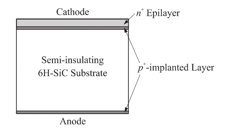
Fig.1 Structure of the proposed 6H-SiC PCSS

Fig.2 Doping profiles of the proposed 6H-SiC PCSS for 2D device simulation

Table 1 Parameters of 6H-SiC for 2D device simulation
2 Results and Discussions
2.1 Effect on the Breakdown Voltage of the Proposed 6H-SiC PCSS
In nature,the high hold-off voltage for semi-insulating 6H-SiC PCSS is sustained by the high resistivity SiC bulk.Generally,for a semiconductor bulk with a resistivity ofρ,the breakdown voltage(VB)iswritten VB= Cρα,here,C andαare both constants.For the positive bias voltage from anode to cathode,the generated holes from the impact ionization in the bulk willmove to the cathode,and are inhibited if a p+layer located at the cathode,which will lead to an improvement of breakdown voltage.
Fig.3 shows the I-V characteristics of the proposed 6H-SiC PCSS,in comparison to Kelkar’s SiC PCSS only with an n+or p+epilayer at the cathode and without the ion implantation layer.The depth and peak concentration for all epilayers are 10μm and 5×1018cm-3,respectively.From the figure,we can see that the breakdown voltages are about 92 kV for the proposed PCSS,66.5 kV for the PCSS only with n+epilayer,and 89.4 kV for the PCSS only with p+epilayer,which shows an improvement of 38.3%or 2.9%in breakdown voltage for the proposed PCSS.This feature will be very beneficial to the application for 6H-SiC PCSS in the areas of high voltage.
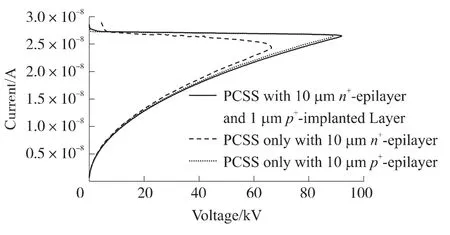
Fig.3 I-V characteristics for three 6H-SiC PCSSs
The higher breakdown voltage for the proposed 6HSiC PCSS can be explained by the distribution of electric field in the PCSS.Fig.4 plots the electric field profiles along the perpendicular cut line from the cathode to the anode for three 6H-SiC PCSSs at their breakdown voltages.From Fig.4(a),we can see that the peak value of electric field for the proposed PCSS is located at the both sides of 6H-SiC bulk,and spreads into the n+epilayer and reaches the cathode.So the breakdown will happen at the cathode,rather than inside the bulk,which contributes to the improvementof breakdown voltage.However,the electric fields in Fig.4(b)for other two PCSSs are less uniform than that of Fig.4(a),and doesn’t extend into the epilayer at the cathode,as a result,the breakdown will occur inside the bulk,which leads to a lower breakdown voltage.

Fig.4 Profiles of Electric field along the cut lines at breakdown voltage
Furthermore,we explore the effectof the n+epilayer thickness on the breakdown voltage of the proposed 6H-SiC PCSS,and the result is plotted in Fig.5.It can be seen that the breakdown voltage linearly increases with the thickness of n+epilayer.The breakdown voltage is 89.6 kV for2μm epilayer,and increases to 92 kV for 10μm epilayer,an improvement of 2.7%.From this result,it seems to be a good way to improve the breakdown voltage of 6H-SiC PCSS by means of increasing the thickness of epilayer.However,the growth rate of SiC epilayer with very lower density of defect by chemical vapor deposition(CVD)over 1700℃ is usually 3μm/h~5μm/h[13-14],so,growth of thicker epilayer will be consuming longer time,which is intolerable for the growth furnace.
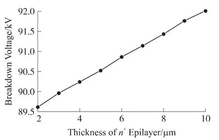
Fig.5 Relationship of breakdown voltage with n+epilayer thickness
2.2 Effect on the On-State Characteristics of the Proposed 6H-SiC PCSS
Inserted between the 6H-SiC bulk and the n+epilayer at the cathode,the p+layer will inhibit holes injected into the cathode,and so,the peak currentof PCSS will decrease.Fig.6 plots the on-state characteristics of the proposed 6H-SiC PCSS,and the PCSSs only with n+or p+epilayers on both sides of the semi-insulating 6HSiC bulk.The thickness of epilayers is 10μm and the doping concentration is 1×1018cm-3.These PCSSs are biased under 1 000 V,the power of incident light is 2 400W,and the wavelength of incident light is 0.4 μm.The optical data for 6H-SiC simulation in Atlas are those from Ref.[15].From the figure,we can see that the peak current of the proposed 6H-SiC PCSS is 3.3 A,lower than the value of 12.7 A for the PCSS only with n+epilayers,buthigher than the value of2.9 A for the PCSS only with p+epilayer.
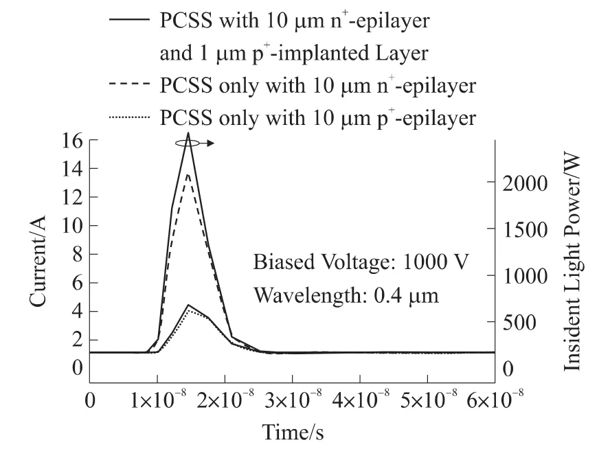
Fig.6 On-state characteristics of three 6H-SiC PCSSs
Subsequently,we exploit the effectof the n+epilayer thickness on the peak currentof the proposed 6H-SiCPCSS,and the thickness of n+epilayers is set to 2,3,4,5,6,7,8,9,10μm,respectively.The bias voltage is 1 000 V,the power of incident light is2 400W,and thewavelength is0.4μm.The result is plotted in Fig.7.From the figure,it can be seen that the peak current first decreases with the increasing of the n+-epilayer thickness,and has a minimum value of 2.4 A at the thickness of 5μm,and then,the peak current begins to increasewith the increasing of the n+-epilayer thickness.
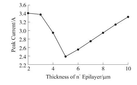
Fig.7 Relationship of peak currentwith n+-epilayer thickness
3 Conclusions
A novel 6H-SiC photoconductor semiconductor switch is proposed,and is characterized with p+ion-implantation layers on the both sides of the semi-insulating(SI)6H-SiC bulk,and an n+epilayer is inserted between the p+ion-implantation and electrodemetal at the cathode.Bymeans of two-dimensional device simulator,the breakdown voltage and on-state characteristics are explored.Simulated results shows that both the breakdown voltage and peak current can be improved by increasing the thickness of n+epilayers,however,it is very difficult to grow thicker epilayer by the semiconductor technology at present.
[1]Zutavern F J,Loubriel G M,O’Malley M W,et al.Photoconductive Semiconductor Switch Experiments for Pulsed Power Applications[J].IEEE Transactions on Electron Devices,1990,37(12):2472-2477.
[2]Schoenberg JSH,Burger JW,Tyo JS,etal.Ultra-Wideband Source Using Gallium Arsenide Photoconductive Semiconductor Switches[J].IEEE Transactions on Plasma Science,1997,25(2):327 -334.
[3]Burger JW,Schoenberg JS,Tyo JS,et al.Photoconductive Semiconductor Switches Used for Ultra-Wideband,High-PowerMicrowave Generation[C]//Proceeding of SPIE,1997,36(1):65-71.
[4]Dogan S,Teke A,Huang D,etal.4H-SiC Photoconductive Switching Devices for Use in High-Power Applications[J].Applied Physics Letters,2003,82(18):3107-3109.
[5]Sheng S,Spencer M,Tang X,etal.Polycrystalline Cubic Silicon Carbide Photoconductive Switch[J].IEEE Electron Device Letters,1997,18(8):372-374.
[6]Zhu K,Dogan S,Moon Y,et al.Effect of n+-GaN Subcontact Layer on 4H-SiC High-Power Photoconductive Switch[J].Applied Physics Letters,2005,86(26):261108-261108-3.
[7]Kelkar K S,Islam N E,Fessler CM,etal.Silicon Carbide Photoconductive Switch for High-Power,Linear-Mode Operations Through Sub-Band-Gap Triggering[J].Journal of Applied Physics,2005,98 (19):093102-093102-6.
[8]Kelkar K S,Islam N E,Kirawanich P,etal.On-State Characteristics of a High-Power Photoconductive Switch Fabricated from Compensated 6-H Silicon Carbide[J].IEEE Transactions on Plasma Science,2008,36 (1):287-292.
[9]Wang Yingmin,Li Juan,Ning Lina,et al.Characterization of Foreign Grain on 6H-SiC Facet[J].Journal of Central South University of Technology,2009,16(3):344-348.
[10]Yang Yan,ZhangWeigang.Chemical Vapor Deposition of SiC at DifferentMolar Ratios of Hydrogen to Methyltrichlorosilane[J].Journal of Central South University of Technology,2009,16(5):730-737.
[11]Kimura M,Inoue S,Shimoda T,et al.Dependence of Polycrystalline Silicon Thin-Film Transistor Characteristics on the Grain-Boundary Location[J].Journal of Applied Physics,2001,89(1):596-600.
[12]Bickermann M,Hofmann D,Straubinger T,et al.Preparation of Semi-Insulating Silicon Carbide by Vanadium Doping during PVT Bulk Crystal Growth[J].Materials Science Forum,2003,433-436:51-54.
[13]Siergiej R R,Clarke R C,Sriram S,et al.Advances in SiCMaterials and Devices:An Industrial Point of View[J].Materials Science and Engineering:B,1999,61-62:9-17.
[14]Kojima K,Okumura H,Kuroda S,et al.Homoepitaxial Growth of 4HSiC on on-Axis(0001)C-Face Substrates by Chemical Vapor Depositon[J].Journal of Crystal Growth,2004,269(2-4):367-376.
[15]ChoykeW J,Palik E D.Handbook of Optical Constants of Solids[M].New York:Academic,1985.
Effects of the n+-Epilayer Thickness on the Electric Characteristics of 6H-SiC Photoconductive Sem iconductor Switch with a Vertical Structure*
ZHOU Yuming*,JIANGHaonan
(School of Electrical Engineering,Anhui University of Technology,Maanshan Anhui243002,China)
6H-SiC photoconductive semiconductor switch(PCSS)with a vertical structure is proposed.The device was characterized with p+ion-implantation layers on the both sides of the semi-insulating(SI)6H-SiC bulk,and an n+epilayer was inserted between the p+ion-implantation layer and electrodemetal at the cathode.Bymeans of two-dimensional(2D)device simulator,the effects of n+-epilayer thickness on electric characteristics of the proposed 6H-SiC PCSS had been exploited,mainly focusing on the breakdown voltage(VB)and on-state characteristics.It is found that the breakdown voltage can be improved by increasing the thickness of n+epilayer.The peak current of on-state just begins to decrease with the increasing of n+-epilayer thickness,and after achieving aminimum value at the thickness of 5μm,the peak current begins to increase.
SiC;photoconductive semiconductor switches;semi-insulating;breakdown voltage
10.3969/j.issn.1005-9490.2013.05.002
TM 89;TN365 文献标识码:A 文章编号:1005-9490(2013)05-0589-05
项目来源:National Natural Science Foundation of China(51177003)
2013-03-07修改日期:2013-04-01
EEACC:2560B
周郁明(1971-),男,汉族,湖北武汉人,博士,副教授,硕士生导师,主要从事电力电子器件及其应用技术的研究,发表论文20余篇,三大检索20余篇,申请发明专利2项,ymzhou@ahut.edu.cn;

姜浩楠(1988-),男,汉族,安徽阜阳人,硕士研究生,主要研究方向为半导体功率器件的设计与测试,jiang_haonan@126.com。