利用钛保护层在ITO电极上直接制备大面积的超薄氧化铝膜
2011-12-12肖立新段来强柴俊一陈志坚龚旗煌
肖立新 段来强 柴俊一 王 芸 陈志坚 曲 波 龚旗煌
(北京大学物理学院,人工微结构和介观物理国家重点实验室,北京100871)
1 Introduction
Since Masuda et al.1,2reported self-organized pore arrangement of anodic aluminum oxide(AAO),AAO film has been intensively investigated as a template for nano materials due to its cost-effective fabrication.3-6However the AAO film fabricated from an Al sheet is too thick(in the order of microns)and not suitable for the fabrication of nano materials with shorter length than 1 μm.7,8In addition,to use and measure the novel properties of nano materials,they should be generally fabricated into devices,i.e.,electrodes need to be fabricated on the nano materials.9,10Therefore it is crucial to fabricate an AAO ultrathin film directly on an electrode.Although efforts have been made to create AAO templates on Si substrates for semiconductor integrated circuits,11-13a transparent electrode needs to be generally used in the field of optoelectronics,e.g.,photovoltaic.14,15However the fabrication of AAO directly on transparent electrodes is relatively few.Early attempts have been made to anodize aluminum layer directly deposited on indium tin oxide(ITO)-coated glass in an acid solution.16,17However this method was difficult to prepare AAO without erosion on the surface of the ITO electrode.Moreover,we found that the Al ultrathin layer was readily to peel off during anodization without a buffer layer.
Recently,double layers of titanium and tungsten were inserted between ITO and Al,fabrication of AAO on ITO-coated glass was achieved.18,19However,the additional tungsten layer decreases its transparency and makes it more complicated for the fabrication.20
A single ultra-thin layer(0.3 nm)of Ti could work as the adhesion/passivation layer(actually not a layer but particles)to prepare an AAO template on ITO glass,21the film was prepared by an electron-beam evaporation and we could not repeat it via a film prepared by a radio frequency(RF)magnetron sputtering.In this work,we inserted a single layer of titanium via a cost-effective of radio frequency(RF)magnetron sputtering between ITO and Al to improve the adhesion and to prevent an erosion on the surface of ITO.The inserting of Ti film can be oxidized to be transparent.Therefore it is highly potential to be used in the fields of photonics,photovoltaics,and nanofabrications.
2 Experimental
2.1 Specimens preparation
ITO-coated glass substrates were routinely cleaned with acetone and ethanol,and treated with oxygen plasma for 1 min before sputtering.Ti layers with thicknesses ranging from 0 to 50 nm at an interval of 5 nm were deposited by RF magnetron sputtering(custom built by KYKY,Beijing,China).Then an Al layer of 300 nm was sputtered on Ti/ITO/glass.Finally a thin layer of transparent tape was applied to the edges ofAl layer to prevent its exposure to the electrolyte,as the edge parts were anodized more quickly than the center parts.
2.2 Anodization of aluminum
The anodization process was previously reported as the following.22The as-deposited specimens were first anodized in 0.3 mol·L-1H2SO4solution at a constant voltage of 20 V for several minutes.Before the specimens became transparent,lifted them out of the electrolyte,then cleaned with deionized water and dried in N2.Followed by dipping them into a mixed solution of 5%(w,mass fraction)H3PO4and 45 g·L-1CrO3at 55-60°C for 6 min to remove the first anodized alumina layer. The specimen was anodized for the second time under the same condition until they became transparent.This two-step anodization process was empolyed here to improve the hexagonal arrangement of the pores,which has been reported before.23,24Finally the specimens were immersed in 5%(w)H3PO4for 15-30 min to widen the pores and to remove the thin barrier layer of alumina at the bottom of the pores.All the above processes were conducted at room temperature;the H2SO4,H3PO4, and CrO3used above were brought from Beijing Chemical Reagent Company,withAR purity.
2.3 Characterizations
SEM(STARTA DB235,FEI company,Oregon,USA)was employed to assess the morphology of the deposited layers and the anodized alumina templates.In order to get clear images of the templates,an ultra-thin layer of chromium was sputtered onto the templates.The UV-visible transmittance spectra were measured by an Agilent 8453E spectrophotometer(Agilent Technologies,Inc.,California,USA).
3 Results and discussion
Fig.1 shows SEM images of the AAO with highly regular pores formed on ITO-coated glass by two-step anodization process of Al(300 nm)/Ti(20 nm)/ITO/glass in a 0.3 mol·L-1H2SO4solution at a constant voltage of 20 V.The porous alumina with straight and parallel channels perpendicular to the substrate was achieved which was approximately 140 nm thick, about half thickness of the original Al film(300 nm).The average pore diameter and the pore interspace were approximately 30 and 60 nm,respectively.A multilayered structure for the film after anodization is clearly demonstrated by a 30°tilted view(Fig.1(c)),in which the AAO and Ti films in the lower part of the image were scraped off carefully.From Fig.1(a),we can see that the ITO layer is well protected without erosion.
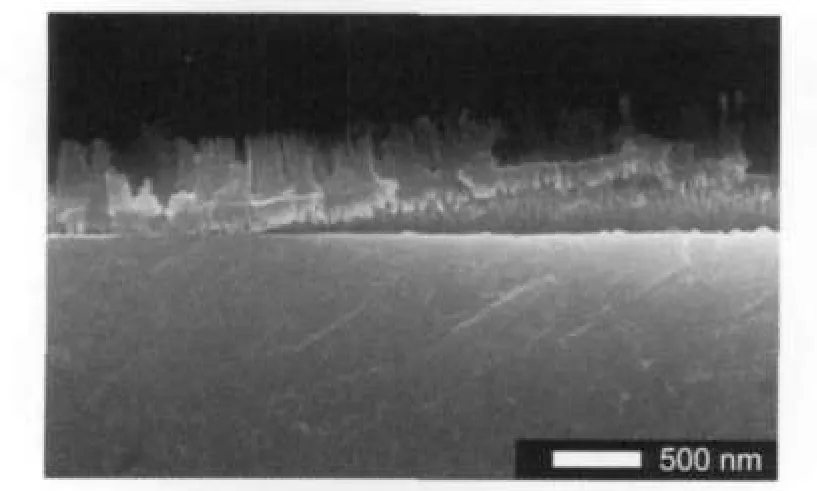
Without a Ti buffer layer,the anodization of Al film sputtered directly on ITO-coated substrate would easily cause Al layer to peel off,then the uncovered ITO layer would be exposed and eroded in the electrolyte under the anodization. Fig.2 clearly illustrates a peeling off of partially anodized Al layer and the destruction of ITO layer.Under the peeling off layer no more ITO layer could be observed.This indicates that an erosion on ITO has been definitely happened,which could be identified by naked eyes and by simply measuring the conductivity of the substrate with a multimeter.In addition,we found that other metals,e.g.,Cr,Au,Ag,and Cu,could not work as the buffer layer to replace Ti.A peeling off or perfora-tion in theAl film did happen during anodization.

Fig.1 SEM images of two-step anodizedAl(300 nm)/Ti(20 nm)/ITO(a)cross-section view,(b)top view,(c)oblique view

Fig.2 Cross-section SEM image of anodizedAl film on ITO without Ti buffer layer in 0.3 mol·L-1H2SO4solution at 20 V
To find the appropriate thickness of Ti buffer layer,a series of Ti layers with thicknesses ranging from 5 to 50 nm were tested,while Al layers remained the same as 300 nm.It was found that the appropriate range is 10-40 nm,beyond which ITO layer will not be protected from erosion.The upper limit of this particular range may be ascribed to the variation in the morphology of Ti layer when its thickness increased,as shown in Fig.3.The naked ITO-coated glass surface was not ideally flat, 20 nm scale bumps can be clearly seen in Fig.3(a).After 5 nm of Ti having been deposited on it,a relative smooth surface was obtained(Fig.3(b)).However because of the crystallization of Ti layer,the roughness increases when its thickness exceeded 40 nm.Fig.3(g)shows that a 50 nm of Ti layer is composed of 20 nm of crystalline grains.As a result,if the Ti layer is thicker than 40 nm,its roughness will cause the interface of Ti and Al layers unconsolidated,thus make Al layer inclined to peel off while anodization.Moreover thicker Ti layer cannot be fully anodized,which will greatly decrease the transparency of the resultantAAO template.

Fig.3 SEM images of Ti/ITO surface with different Ti layer thicknesses(a)0 nm,(b)5 nm,(c)10 nm,(d)25 nm,(e)30 nm,(f)40 nm,(g)50 nm
To understand the buffer effect of Ti during anodization,a 20 nm of Ti film was sputtered on the ITO-coated glass and then anodized in 0.3 mol·L-1H2SO4at 20 V for about 5 min. We found that the anodization rate of Ti was lower than that of Al.Pores with 10 μm scale could be observed in the SEM images shown in Fig.4.Thus the anodization of Ti layer can be identified.Because the anodization of Ti proceeds at a lower speed than that of Al,it can block H2SO4from reaching ITO layer for a certain time,thus the other parts of Al layer can continue anodization until the Al layer completely anodized.However if the thickness of Ti layer is less than 10 nm,it cannot block H2SO4during the time before Al is fully anodized.This is not the situation reported by Hu et al.21to prepare an AAO template on ITO glass with an ultrathin(0.3 nm)adhesion/passivation layer of Ti by electron-beam evaporation,which might be interpreted with the higher quality film prepared by electron-beam evaporation than by RF magnetron sputtering. Though we can stop reaction when the current starts to decrease,some parts of the film are not fully anodized.We can clearly observe that some parts remain opaque with metallic color.

Fig.4 SEM images of Ti(20 nm)layer on ITO-coated glass anodized in 0.3 mol·L-1H2SO4at 20 V for about 5 min
Fig.5 shows cross-section SEM images of the templates with different thicknesses of Ti layer ranging from 10 to 40 nm.A representative top view is given in Fig.5(g).All samples were anodized using the two-step anodization process as described above.All the templates showed almost the same pore diameter and pore density,and the highly regulated pores were vertically open to the substrates with relatively smooth surface.The thickness of Ti buffer layer increased to nearly 3 times after anodization,suggesting that Ti had been oxidized.It is consistent with the result reported by Tang et al.25that a titanium layer could be anodized on fluorine-doped tin oxide conducting glass and obtained TiO2nanotube arrays.This is very different from the situation where Ti is used as buffer layer between Al layer and Si substrate,in which the author concluded that Ti had not been oxidized.13In our case,the oxidation of Ti may be due to the high conductivity of ITO film.Thus the transparency of the resultant AAO template is improved after the oxidation of Ti buffer layer and benefit to the usage in the field of photonics and optoelectronics.

Fig.5 Cross-section(a-f)and top view(g)SEM images of two times anodizedAl(300 nm)/Ti/ITO with different Ti layer thicknesses(a)10 nm,(b)15 nm,(c)20 nm,(d)25 nm,(e)35 nm,(f)40 nm,(g)top view ofAAO with 25 nm Ti layer

Fig.6 Transmittance of specimens with(A)various Ti layer thicknesses and(B)different anodization conditions
The UV-visible transmittance spectra of the as-deposited Ti/ ITO with a series of Ti layer thicknesses and anodized Al/Ti/ ITO with different anodization times are shown in Fig.6.Fig.6 (A)shows that the transmittance of specimens decreases greatly when Ti layer thickness increases from 10 to 35 nm;the best transmittance of 74%is got from Ti layer thickness of 10 nm at 440 nm wavelength.The transmittance was increased by using two-step anodization process instead of one-step anodization (Fig.6(B)).This was consistent with what we expected as the AAO layer prepared by the two-step anodization process should be thinner.Therefore,10-20 nm of Ti buffer layer via the two-step anodization process is suitable for the usage in the field of high transparency.
4 Conclusions
We demonstrate a feasible method to directly fabricate an ultrathin AAO film(~140 nm)with a large size(about 4 cm2)on transparent conducting ITO-glass substrate.The average pore diameter and the pore inter-space were approximately 30 and 60 nm,respectively.A special chosen of Ti buffer layer(thickness 10-40 nm)between Al layer and ITO substrate plays a critical role in improving adhesion and ensuring ITO protection which could not be replaced by other metals,e.g.,Cr,Au, Ag,and Cu(which we have tested).But there is possibility that some metals whose oxides are not soluble in acid may play the same role as Ti.UV-visible transmittance spectra confirmed that the Ti buffer layer was oxidized and the resultant AAO templates showed relative high transmittance.A Ti buffer layer with 10-20 nm of thickness via the two-step anodization process is suitable for the usage in the field of high transparency. The method developed in this work may be adapted for further fabrication of various structures such as nanorod or nanotube arrays on transparent electrode for devices.
(1) Masuda,H.;Fukuda,K.Science 1995,268,1466.
(2) Masuda,H.;Hasegwa,F.;Ono,S.J.Electrochem.Soc.1997, 144,L127.
(3)Guo,Y.Y.;Wang,M.;Mao,X.B.;Jiang,Y.X.;Wang,C.;Yang, Y.L.Acta Phys.-Chim.Sin.2010,26,203. [郭元元,汪 明,毛晓波,蒋月秀,王 琛,杨延莲.物理化学学报,2010,26, 203.]
(4) Yanagishita,T.;Sasaki,M.;Nishio,K.;Masuda,H.Adv.Mater. 2004,16,429.
(5) Johansson,A.;Widenkvist,E.;Lu,J.;Boman,M.;Jansson,U. Nano Lett.2005,5,1603.
(6) Shukla,S.;Kim,K.T.;Baev,A.;Yoon,Y.K.;Litchinitser,N. M.;Prasad,P.N.Nano Lett.2010,4,2249.
(7) Li,A.P.;Müller,F.;Birner,A.;Nielsch,K.;Gösele,U.J.Appl. Phys.1998,84,6023.
(8) Lee,W.;Ji,R.;Gösele,U.;Nielsch,K.Nat.Mater.2006,5,741.
(9)Shirota,Y.;Kageyama,H.Chem.Rev.2007,107,953.
(10)Xia,Y.N.;Yang,P.D.;Sun,Y.G.;Wu,Y.Y.;Mayers,B.;Gates, B.;Yin,Y.D.;Kim,F.;Yan,Y.Q.Adv.Mater.2003,15,353.
(11) Hobbs,K.L.;Larson,P.R.;Lian,G.D.;Keay J.C.;Johnson, M.B.Nano Lett.2004,4,167.
(12) Sander,M.S.;Tan,L.S.Adv.Funct.Mater.2003,13,393.
(13)Tian,M.L.;Xu,S.Y.;Wang,J.G.;Kumar,N.;Wertz,E.;Li, Q.;Campbell,P.M.;Chan,M.H.W.;Mallouk,T.E.Nano Lett. 2005,5,697.
(14) Teh,L.K.;Furin,V.;Martucci,A.;Guglielmi,M.;Wong,C.C.; Romanato,F.Thin Solid Films 2007,515,5787.
(15) Chuang,L.M.;Fu,H.K.;Chen,Y.F.Appl.Phys.Lett.2005,86, 061902.
(16) Chu,S.Z.;Wada,K.;Inoue,S.;Todoroki,S.J.Electrochem. Soc.2002,149,B321.
(17) Chu,S.Z.;Wada,K.;Inoue,S.;Hishita,S.;Kurashima,K. J.Phys.Chem.B 2003,107,10180.
(18) Musselman,K.P.;Mulholland,G.J.;Robinson,A.P.; Schmidt-Mende,L.;MacManus-Driscoll,J.L.Adv.Mater. 2008,20,4470.
(19)Ren,X.;Gershon,T.;Iza,D.C.;Munoz-Rojas,D.;Musselman, K.;Macmanus-Driscoll,J.L.Nanotechnology 2009,20,365604.
(20) Kuo,C.Y.;Tang,W.C.;Gau,C.;Guo,T.F.;Jeng,D.Z.Appl. Phys.Lett.2008,93,033307.
(21) Foong,T.R.B.;Sellinger,A.;Hu,X.ACS Nano 2008,2,2250.
(22) Xiao,L.X.;Duan,L.Q.;Luo,F.W.;Chen,Z.J.;Gong,Q.H. AWay to Fabricate anAAO Template and the Corresponding Device Directly on a Transparent electrode.CN Patent 200810224414.7,2008-10-14.[肖立新,段来强,罗方闻,陈志坚,龚旗煌.在透明电极上制作AAO模板的方法及相应器件:中国,CN200810224414.7[P].2008-10-14.]
(23) Masuda,H.;Yada,K.;Osaka,A.Jpn.J.Appl.Phys.1998,37, L1340.
(24) Li,A.P.;Müller,F.;Birner,A.;Nielsch,K.;Gösele,U.Adv. Mater.1999,11,483.
(25)Tang,Y.X.;Tao,J.;Zhang,Y.Y.;Wu,T.;Tao,H.J.;Bao,Z.G. Acta Phys.-Chim.Sin.2008,24,2191.[汤育欣,陶 杰,张焱焱,吴 涛,陶海军,包祖国.物理化学学报,2008,24,2191.]
