新一代STE分子束外延系统
2010-10-24AlexeevFilaretovChalyYuPogorelsky
A.Alexeev,A.Filaretov,V.Chaly,Yu.Pogorelsky
(“Semiconductor Technologies and Equipment”JSC)
In 2001,"Semiconductor Technologies and Equipment" JSC (St.Petersburg,Russia) started to manufacture new generation of MBE systems (trademark "STE") (Fig.1).This company was founded by technologists from Ioffe Institute that have great practical experience on domestic and foreign MBE systems.Projection of new MBE systems started in 1995.

Fig.1 STE3N3 MBE system
The company started its activities with the development of special MBE systemintended for growth of III-N semiconductor compounds (in 1990-2000's,nitride semiconductors have demonstrated new opportunities in optoelectronics and microwave microelectronics).It was found that their growth conditions differ from the growth conditions of classical semiconductors A3B5(eg,AlGaAs).Attempts of traditional MBE systems adaptation for this purpose did not reach desired results.The significant increase of the wafer temperature,serious amplification of pumping system for removing ammonia flow used as a nitrogen source,etc.were required.(In particular for the nitrides,it led to world time lag in MBE technology if compare to MOCVDmethods).
Developers of"Semiconductor Technologies and Equipment"JSC were success to solve the above problems.STE3N2(Fig.2)and STE3N3 MBEsystems demonstrate high level of technological and instrumental results comparable to MOCVDsystems of foreign production.
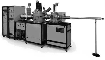
Fig.2 STE3N2 MBE system
The first testing of established MBE system was held at "Svetlana-Rost" JSC (St.Petersburg,Russia),specialized on the development and serial manufacture of semiconductor heterostructures,microwave transistors and integrated circuits.Developed nitride heterostructures for microwave microelectronic show the complete lack of collapse effect (power decrease in the microwave regime in compared with the static characteristics),that is typical for nitride transistors.Mobility in two-dimensional channel on GaN/AlGaN heterointerface is~1500 cm-2/V·s at concentration~1,5·1013cm-2.(Note that the carrier concentration exceeds an order than the maximum values for the structures based on AlGaAs).Dispersion of specific layer resistance Rson a plate no more than ± 1,5%,which determines the high output in the transistors manufacture(Fig.3).
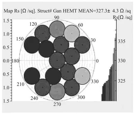
Fig.3 GaN HEMT(φ76 mm)
In cooperation with Federal State Enterprise "Istok" transistors were fabricated on these heterostructures with the power density of 3.8 W/mm at 10 GHz,that is close to the limit values for the structures grown on sapphire.The achievement of these results is largely due to the capacity of growth equipment.STE3N2 and STE3N3 systems provide maximum value of the sample temperature not lower than the 1 200℃that at least at 200℃higher than on GaN-oriented system Compact-21 produced by "Riber" (France) -one of the world leaders in this sphere.The ability to carry out the process at 1 200℃gives the possibility to grow heterostructures with AlN sublayer that has high crystal perfection.Voluminous GaN structure grown on such layer shows record value of the free carriers'mobility (Fig.4).This basic material characteristic is usually higher for MOCVD technology than for MBE.The results obtained on STE3N2 system are on the best level of the published data both for traditional MBE equipment and for MOCVD technology(growth on sapphire).
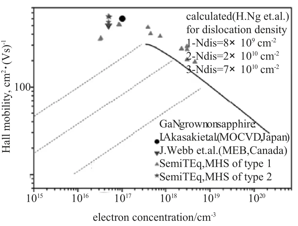
Fig.4 STE3N:volume-doped GaN-results
The important instrument aspect of AlN sublayer growth process is the possibility of its easy adaptation to different wafer types:sapphire,silicon,silicon carbide.High thermal conductivity of Si wafers (especially SiC) can significantly reduce the effects of thermal heating on the power transistor operation.
These results are provided by the features of the created equipment.
600 mm diameter growth reactor includes:
●Manipulator that provides heating and rotation of wafer fixed in the holder of patented design with diameter to 100 mm;
●Two cryopanels with liquid nitrogen;
●Seven ports for e ffusion sources with shutters and one central port for ammonia injector;
●System of high-energy electron diffraction,optical pyrometer,specialized laser interferometer,mass spectrometer.
Reactor pumping system consists of:corrosion-resistive turbo-molecular pump,ion pump and oil-free scroll pumping system.
Service chambers(one in STE3N2,two in STE3N3):load-lock chamber with eight samples'storage,additional preparation chamber that provides heating and degassing of wafer before growth.Each chamber has its own pumping system and combines by linear manipulators that transfer the samples fromone chamber toanother.
During growth process the following control functions are realized:
*Temperature of each source given with an accuracy of±0,5℃;
● Manipulating of the source shutters,open/close duration is less than 0.3 s;
●Ammonia feed flow carried out with an accuracy of less than 2%;
●Wafer temperature maintained with an accuracy of±0,5℃.
●The process is fully automated,but can be done manually(on PC).
We should also note on the original design of gallium and aluminum effusion sources that takes into account their operation specifics in ammonia atmosphere and ensure long-term performance combined with high rates of AlN and GaN growth(>1 micron/h).
Sources design as well as a number of critical technology solutions in MBE systems are patented.
Testing of main STE3N2 systemin"Svetlana-Rost,JSC"was aimed not only the technology approbation but also the design reliability.After year-lon g exploitation and more than three hundred epitaxial process serial production STE3N2 and STE3N3 systems was started.
To date the overall distribution:
●STE3N2 for"Svetlana-Rost"JSC;
●STE3N2 for Ioffe Institute;
●Three modules of STE3N3 installed to the robotic production cluster of"NT-MDT"JSC for Moscow Institute of Electronic Technology(Zelenograd);
●Multi-chamber complex includes STE3N3 system for the Kurchatov Scientific Center with "Sigma-Scan"JSC(Moscow);
●STE3N3 for"Svetlana-Rost"JSC;
STE3N3 for Institute of Microstructure Physics(Nizhny Novgorod);
●STE3532 for Southern Federal University(Taganrog);
●STE3526 for Ioffe Institute
●Three new orders started to develop.
Systems' installation in Ioffe Institute and MIET accompanied with growing of test structures with GaN interior layers and double heterostructure of transistor type.Parameters of test samples coincided with the above characteristics for the structures grown on main STE3N2 systemin"Svetlana-Rost"JSC.
"Semiconductor Technologies and Equipment"JSC besides nitride MBE systems has mastered the production of MBE equipment for classical A3B5/A2B6 semiconductors (Fig.5),electron beam evaporation systems,plasma chemical etching and plasma chemical vapor deposition systems,rapid thermal annealing systems of semiconductor wafers.

Fig.5 STE3532 MBE system
The latest project of MBE equipment is Two-Growth Chamber complex STE3526 that specially designed as a modern MBE technology platform for hybrid III-V and II-VI semiconductor heterostructures growing(Fig.6).

Fig.6 STE3526 MBE complex
Each of these systems was delivered to Russian research centers and enterprises.
Supply and maintenance experience allows to plan an active campaign to exit the company with its products on foreign markets.To this aim,"Semiconductor Technologies and Equipment" JSC has already hosted a European office(SemiTEq GmbH).