Improvement of Ga2O3 vertical Schottky barrier diode by constructing NiO/Ga2O3 heterojunction
2024-04-23XueqiangJiJinjinWangSongQiYijieLiangShengrunHuHaochenZhengSaiZhangJianyingYueXiaohuiQiShanLiZengLiuLeiShuWeihuaTangandPeigangLi
Xueqiang Ji, Jinjin Wang, Song Qi, Yijie Liang, Shengrun Hu, Haochen Zheng, Sai Zhang,Jianying Yue, Xiaohui Qi, Shan Li, Zeng Liu,†, Lei Shu, Weihua Tang,†, and Peigang Li,†
1School of Integrated Circuits & State Key Laboratory of Information Photonics and Optical Communications, Beijing University of Posts and Telecommunications, Beijing 100876, China
2College of Integrated Circuit Science and Engineering, Nanjing University of Posts and Telecommunications, Nanjing 210023, China
3Beijing Microelectronics Technology Institute, Beijing 100076, China
Abstract: The high critical electric field strength of Ga2O3 enables higher operating voltages and reduced switching losses in power electronic devices.Suitable Schottky metals and epitaxial films are essential for further enhancing device performance.In this work, the fabrication of vertical Ga2O3 barrier diodes with three different barrier metals was carried out on an n—-Ga2O3 homogeneous epitaxial film deposited on an n+-β-Ga2O3 substrate by metal-organic chemical vapor deposition, excluding the use of edge terminals.The ideal factor, barrier height, specific on-resistance, and breakdown voltage characteristics of all devices were investigated at room temperature.In addition, the vertical Ga2O3 barrier diodes achieve a higher breakdown voltage and exhibit a reverse leakage as low as 4.82 ×10⁻⁸ A/cm2 by constructing a NiO/Ga2O3 heterojunction.Therefore, Ga2O3 power detailed investigations into Schottky barrier metal and NiO/Ga2O3 heterojunction of Ga2O3 homogeneous epitaxial films are of great research potential in high-efficiency, high-power, and high-reliability applications.
Key words: Ga2O3; Schottky barrier diode; NiO/Ga2O3 heterojunction
1.Introduction
The utilization of power electronic devices will be crucial in future applications involving high temperatures, high voltages, and high radiation levels, where conventional siliconbased devices encounter limitations[1].Power devices based on wide bandgap (WBG) materials, particularly silicon carbide (SiC) and gallium nitride (GaN), have undergone a revolution in recent years, supplementing the lack of growth of silicon-based power electronics in the medium- and high-voltage markets[2-4].The ultra-wide band gap semiconductor gallium oxide (Ga2O3) exhibits a larger band gap (~4.9 eV),higher breakdown field strength (8 MV/cm), and superior Baliga's figure of merit (>3000) compared to SiC and GaN,thereby highlighting its immense potential in the realm of ultra-high voltage applications[5-7].The current availability of a well-established, cost-effective, high-quality, and large-scale substrate and epitaxial material product forβ-Ga2O3greatly facilitates the advancement of Ga2O3power electronic devices[8-11].
In recent years, the rapid development of verticalβ-Ga2O3Schottky barrier diodes (SBDs) can be attributed to the availability of commercial Ga2O3materials and the ability to achieve highly controllable electrical conductivity[12,13].The conventional configuration of Ga2O3SBDs typically consists of a vertical structure, wherein Ga2O3forms a Schottky contact with the anode metal and an ohmic contact with the cathode metal[14].Furthermore, the Schottky barrier plays a crucial role in the electron transport process, thus it is imperative to carefully select an appropriate anode metal to achieve optimal performance of the SBD device.The barrier heights for contacts of various work function barrier metals, such as Au, Ni, Gu, Mo, W, Pd, etc., in contact with Ga2O3have been extensively studied[15-17].It is worth noting that the observed differences in results are minimal and may contribute to the Fermi pinning effect at the surface/interface of Ga2O3[17-19].However, the electrical properties of Ga2O3SBDs require further investigation.In addition, the current focus of research lies in the exploration of Ga2O3pn heterojunction diode devices (HJDs) with alternative p-type material substitutions,owing to the more difficult p-type doping.The current focus of research lies in NiO, which is widely regarded as the most suitable choice due to its controlled p-type doping with a bandgap of 3.6-4.0 eV[20-23].The pn junction diodes exhibit outstanding performance in terms of their ability to withstand reverse voltage and minimize leakage current.Thus,the enhancement of the reverse electrical characteristics of NiO/Ga2O3HJDs warrants dedicated investigations.
In this work, the verticalβ-Ga2O3SBDs device was prepared without a termination structure, and the anode electrodes were chosen from high-work function barrier metals such as Au, Ni, and Pd.In comparison with Ga2O3SBDs, the barrier metals of Ni/Au showed better forward current output electrical performance with an on resistance (Ron) of 0.11 Ω·cm2, built-in voltage (Vbi) of 1.47 V, and ultra-low leakage current.In addition, the advantages of NiO/Ga2O3HJDs in terms of enhanced breakdown voltage and reduced leakage are further confirmed through TCAD simulations and experiments.This work provides some guidance for the electrode selection and optimization of future Ga2O3SBDs.
2.Experiment
The homogeneous n-Si-dopedβ-Ga2O3epitaxial films with a thickness of 1.45μm were fabricated using an MOCVD on n+(100) Sn-doped substrate with a carrier concentration(Nd) of 5 × 1018cm-3.Ga2O3single crystal substrates and epitaxial wafers used in this research project are from Beijing GAO Semiconductor Co.Ltd.The Schottky barrier diode (SBD)was fabricated by depositing anode electrodes of various metals (Pd/Au, Ni/Au, Au) via sputtering, with each electrode measuring 600μm × 600μm.Ti/Au (50/100 nm) was used as the cathode back electrode.
The crystal structure and rocking curve peak of the sample were evaluated via X-ray diffraction (XRD) patterns.The optical absorption was characterized using a ultraviolet-visible (UV-Vis) spectrophotometer.The surface morphologies and roughness of all samples were investigated by scanning microscope (SEM) and atomic force microscopy (AFM).The thickness of the film was determined by a step profiler (KLA D-300).The capacitance-voltage (C-V) and current-voltage(I-V) characteristics of the device were tested by using a semiconductor analyzer (Keithley, 4200-SCS).
3.Results and discussion
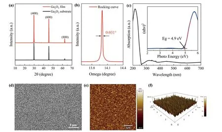
The XRD patterns of the Ga2O3film and substrate exhibit typicalβ-Ga2O3structure with single orientations of (400),(600), and (800), as depicted in Fig.1(a).The X-ray rocking curve peak of Ga2O3film from the (400) plane exhibited an FWHM of 111.6 arcsec, as shown in Fig.1(b), indicating excellent crystalline properties of theβ-Ga2O3film[24,25].The UV-Vis absorption spectra observed are also presented in Fig.1(c).Based on the analysis, the bandgap of theβ-Ga2O3films was determined to be 4.9 eV, which aligns well with the findings reported in previous research[26-28].The SEM and AFM surface morphology of theβ-Ga2O3film is depicted in Figs.1(d)-1(f).The results demonstrate that the surface of theβ-Ga2O3film exhibits a clean, uniform, and atomically flat structure.

Fig.1.(Color online) (a) XRD pattern, (b) rocking curve peak from the (400) plane, (c) absorption spectra, (d) surface SEM image, and the surface AFM of (e) 2D and (f) 3D image of β-Ga2O3 films.
Fig.2(a) illustrates the schematic cross-sectional view of the fabricated verticalβ-Ga2O3SBD without a terminal structure.The anode electrodes for verticalβ-Ga2O3SBD were deposited using magnetron sputtering with Pd/Au, Ni/Au,and Au as the Schottky contact, respectively.All of these electrodes have work functions exceeding 5 eV.The epitaxial film is grown using the MOCVD technique, and a film thickness of 1.45μm was investigated by a step profiler.The carrier concentration (Nd) of the film is approximately 2.6 × 1016cm-3, as obtained from Fig.2(b).TheNdcan be estimated by extracting the slope from the1/C2-Vcurve, which can be described by following Eqs.(1) and (2)[29].

Fig.2.(Color online) (a) The schematic cross-sectional image for the vertical β-Ga2O3 SBD, (b) C-V characteristics of β-Ga2O3 SBD, and extracted Nd of inset.
The Sn-doped substrate with a (100) orientation has a thickness of approximately 500μm and aNdof 5 × 1018cm-3.Ti/Au electrodes serve as the ohmic contacts on the backside.
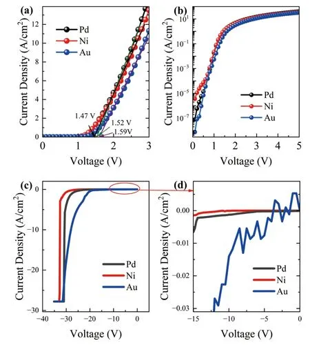
The electrical performance of all devices was assessed by conducting forward and reverse current density-voltage(J-V) measurements on vertical Ga2O3SBDs, as illustrated in Fig.3.All devices exhibit slightly different forward electrical properties.Theβ-Ga2O3SBDs with Pd, Ni, and Au electrodes exhibit respective built-in voltages (Vbi) of 1.52, 1.47, and 1.59 V,which were determined by extracting the intercept from the linear fitting of theJ-Vcurve shown in Fig.3(a).TheRonofβ-Ga2O3SBDs with Pd, Ni, and Au electrodes is determined as 0.09, 0.11, and 0.12 Ω·cm2, respectively, based on the slope of the linear region in theJ-Vcharacteristics.Additionally, all devices exhibit comparable saturation currents, as illustrated in Fig.3(b).According to the theory of thermal electron emission (TE) mode[30,31], theJ-Vcharacteristic of the Schottky diode can be described by the following equations.

Fig.3.(Color online) Forward J-V characteristics of three different Ga2O3 SBDs in (a) linear and (b) logarithmic plots; (c) reverse J-V characteristics of Ga2O3 SBDs and (d) local enlargement from 0 to -15 V.
whereeis the electron charge,nis the ideality factor,Kis the Boltzmann constant,JSis the saturation current,Ais the contact area,A*is the Richardson constant, andΦJ-Vis the Schottky barrier height.Therefore, the ideality factor (n) and Schottky barrier height (ΦJ-V) can be estimated by extracting from Eqs.(3) and (4), which can be described as:
The comparison ofnandΦJ-Vforβ-Ga2O3SBDs is summarized in Table 1.Although thenof an ideal Schottky diode is equal to 1, in practice, the values of all samples, as indicated in Table 1, surpassing the threshold of 3, signify a more pronounced deviation from the TE model in terms of the current conduction mechanism.The first possibility is that there might exist additional conduction mechanisms, such as fieldemitting (FE) or thermal field-emitting (TFE), which contribute to the current transport and result inJ-Vcharacteristics of the device that deviate from those predicted by the single thermionic emission (TE) model[32].On the contrary, an alternative explanation arises from the presence of dislocations or defects in the material, leading to lateral inhomogeneity of the Schottky barrier height and consequently resulting in this relatively high ideal factor[19,33].Similarly, theΦJ-Vof theβ-Ga2O3Schottky contact is affected by different conduction mechanisms and material defects.Therefore, the work function of the metal itself can not directly determine thenandΦJ-Vof the contact between the barrier metal andβ-Ga2O3.

Table 1.The summary of electrical performances for β-Ga2O3 SBDs and HJDs.
Due to the relatively simple device structure, verticalβ-Ga2O3SBDs exhibit comparatively lower withstand voltages,with breakdown voltages of 33 V for Ni electrode devices,30.8 V for Pd electrode devices, and 31.5 V for Au electrode devices, as depicted in Fig.3(c).As observed from the local enlargement in Fig.3(d), theβ-Ga2O3SBDs with Ni electrode exhibit a reduced reverse leakage current.The utilization of Ni Schottky electrodes is highly recommended for enhancing the electrical characteristics ofβ-Ga2O3SBDs.Overall, a comparison of the parameters from the table reveals that there is no significant correlation between the electrical performance ofβ-Ga2O3SBDs and the calculated values ofnandΦJ-Vin ET mode.Furthermore, it suggests that multiple factors influence the electrical performance ofβ-Ga2O3SBDs.
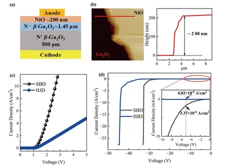
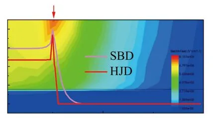
The device performance is further enhanced through the utilization of NiO/β-Ga2O3heterojunction diodes (HJDs), the device schematic is shown in Fig.4(a).Based on the AFM images, a 200 nm thick NiO film was obtained, as illustrated in Fig.4(b).Compared with theβ-Ga2O3SBDs, the positive electrical characterization properties of NiO/β-Ga2O3HJDs decline due to hole injection from the NiO, as shown in Fig.4(c).However, the breakdown voltage of the NiO/β-Ga2O3HJDs has been enhanced from 33 to 44.5 V, and the reverse leakage current is significantly reduced from 3.37 × 10⁻⁶to 4.82 × 10⁻⁸A/cm2, as illustrated in Fig.4(d).Additionally, the TCAD simulation has confirmed that both theβ-Ga2O3SBDs and NiO/β-Ga2O3HJDs exhibit an electric field peak precisely at the edge of the Schottky electrode.Furthermore, the incorporation of heterogeneous film NiO effectively alleviates the concentration of electric field at the edges, as depicted in Fig.5.Therefore, the breakdown voltage of NiO/β-Ga2O3HJDs increases greatly.

Fig.4.(Color online) (a) The schematic cross-sectional image for the NiO/β-Ga2O3 HJD, (b) AFM image, (c) forward J-V characteristics, (d) reverse J-V characteristics of SBDs and HJDs.

Fig.5.(Color online) Simulation results of the lateral electrostatic field for the β-Ga2O3 SBDs and NiO/β-Ga2O3 HJDs.
4.Conclusion
In this study, the fabrication of verticalβ-Ga2O3with different barrier metals was carried out on homogeneous epitaxial films by using MOCVD technology, excluding the use of edge terminals.The results show that the vertical Ga2O3SBDs with Ni electrodes showed better forward current output electrical performance and maintained a reduced reverse leakage current.Additionally, we further enhance the breakdown voltage of the device by fabricating NiO/β-Ga2O3HJDs and significantly reduce the reverse leakage current of the device from 3.37 × 10⁻⁶to 4.82 × 10⁻⁸A/cm2.Our results show that Ga2O3power detailed investigations into Schottky barrier metal and NiO/Ga2O3heterojunction of Ga2O3homogeneous epitaxial films are of great research potential in high-efficiency, highpower, and high-reliability applications.
Acknowledgments
This work was supported by BUPT Excellent Ph.D.Students Foundation (CX2023301) and in part by the National Natural Science Foundation of China (62204019).The authors thank Beijing GAO Semiconductor Co.Ltd.for providing Ga2O3single crystal substrates and epitaxial wafers utilized in this research project.
杂志排行
Journal of Semiconductors的其它文章
- Chemical vapor deposition for perovskite solar cells and modules
- Highlights in recent wireless power IC research
- Recent advancements in continuously scalable conversion-ratio switched-capacitor converter
- Towards efficient generative AI and beyond-AI computing:New trends on ISSCC 2024 machine learning accelerators
- Millimeter-wave PA design techniques in ISSCC 2024
- Light-emitting devices based on atomically thin MoSe2
