Purification of copper foils driven by single crystallization
2024-02-29JinZongKou寇金宗MengZeZhao赵孟泽XingGuangLi李兴光MengLinHe何梦林FangYouYang杨方友KeHaiLiu刘科海QingQiuCheng成庆秋YunLongRen任云龙CanLiu刘灿YingFu付莹MuHongWu吴慕鸿KaiHuiLiu刘开辉andEnGeWang王恩哥
Jin-Zong Kou(寇金宗), Meng-Ze Zhao(赵孟泽), Xing-Guang Li(李兴光), Meng-Lin He(何梦林),Fang-You Yang(杨方友), Ke-Hai Liu(刘科海), Qing-Qiu Cheng(成庆秋),Yun-Long Ren(任云龙), Can Liu(刘灿), Ying Fu(付莹),‡,Mu-Hong Wu(吴慕鸿),7,§, Kai-Hui Liu(刘开辉),,7, and En-Ge Wang(王恩哥),7,8
1Songshan Lake Materials Laboratory,Dongguan 523808,China
2Beijing National Laboratory for Condensed Matter Physics,Institute of Physics,Chinese Academy of Sciences,Beijing 100190,China
3Guangdong Provincial Key Laboratory of Quantum Engineering and Quantum Materials,School of Physics,South China Normal University,Guangzhou 510006,China
4Guangdong–Hong Kong Joint Laboratory of Quantum Matter,Frontier Research Institute for Physics,South China Normal University,Guangzhou 510006,China
5State Key Laboratory for Mesoscopic Physics,Frontiers Science Center for Nano-optoelectronics,School of Physics,Peking University,Beijing 100871,China
6Key Laboratory of Quantum State Construction and Manipulation(Ministry of Education),Department of Physics,Renmin University of China,Beijing 100872,China
7International Center for Quantum Materials,Collaborative Innovation Center of Quantum Matter,Peking University,Beijing 100871,China
8School of Physics,Liaoning University,Shenyang 110036,China
Keywords: purification,copper foil,thermal annealing technique,single crystallization
1.Introduction
The pursuit on metals of high purity is in high demand for the development of advanced precision electronics due to the excellent intrinsic properties of pure metals.[1–4]Among them, high-purity copper, with its attractive electronic, thermal, and mechanical performances, has been widely used in the modern industry of communications,[5–7]electronics,[8–10]solar cells,[11–13]and national defense.[14]Purification of copper has been demonstrated to be an effective way to further increase the performance of products.For example, the graphene quality can be increased through the utilization of high-purity Cu,[15–17]the reduction in area after a tensile test of 6N Cu(91%)is higher than that of commercial Cu with 3N purity (82%),[18]and the electrical conductivity can increase almost 100 times when purification from 4N to 7N at 10 K.[19]
To address the demand for high-purity Cu, a range of purification techniques have been developed,[20–25]predominantly including two approaches: (i) dissolving the pure Cu in high-purity acids followed by subsequent purification through liquid–liquid separation involving electrolyte[26,27]or anion exchange.[28,29]However, these methods can only be adopted for raw material reconstruction and also suffer from contaminants of diaphragm slimes or organic ions; (ii) zone melting,[30–32]which heavily relies on multiple passes with heating elements,leading to issues of low efficiency and high energy consumption.None of the above purification methods are suitable for as-produced Cu products, such as rolled Cu foils.Therefore, a convenient method to further purify the as-received copper products without destructing their initial macroscopic structures is of great expectation to be developed.
In this work,we developed a temperature-gradient-driven single crystallization method to purify commercial 3N rolled Cu foils into 4N high-purity counterparts.The temperature gradient at the interface between the liquid and solid area around the central hot zone performs as the driving force for the continuous motion of grain boundaries on the Cu surface,leading to the crystallization of polycrystals.[33]Meanwhile,the impurities dissolved in the polycrystal Cu would be propelled along with the boundary movement, and finally anchored on the localized edges.On the other hand, the high temperature can also facilitate the evapouration of elements with high saturated vapour pressure.[34,35]A series of mass spectrometric results unambiguously demonstrated the higher purity of 4N,along with the improved mechanical and electrical properties.This work provides an accessible way for the purification of commercial Cu products in a maneuverable and low-cost manner.
2.Methods
In our experiment, the polycrystal Cu foil (25-µm thick,purity level of 99.98%) was positioned atop a highly refined graphite substrate (TOYO TANSO Co., Ltd), which was further situated onto a substrate composed of exceptionally pure quartz (purity level of 99.9999%, Jinzhou East Quartz Material Co.,Ltd.).Subsequently,the composite arrangement was loaded into a chemical vapor deposition(CVD)furnace(Tianjin Kaiheng Co.,Ltd.,customer-designed).The central region of the furnace was set to achieve an annealing temperature of 1065◦C (∼18◦C below the Cu melting point) with a flow of 600-sccm Ar and 38-sccm H2.After annealing,the system was naturally cooled down to room temperature under identical gas conditions.
We use the nanoscale secondary ion mass spectrometry (Nano-SIMS) to characterize the variation of impurities.Impurities concentration measurements are performed using glow discharge mass spectrometry (GDMS) and inductively coupled plasma mass spectrometry (ICP-MS).Nanoindentation experiments are operated by Bruker’s Hysitron TI 980 TriboIndenter at 1000µN,and mechanical properties results are obtained by an electromechanical universal testing machine system (Shenzhen Wance Testing Machine Co., Ltd.) with a tensile rate of 0.05 mm/min.
3.Results and discussion
Figure 1(a) illustrates the schematic of the method employed.Along the axis of the quartz tube, a subtle temperature gradient is established, leading to varying temperatures for distinct segments of the same Cu foil,[33,36]i.e., the central region is in high temperature(HT),while the two adjacent sides are in low temperature(LT).The thermal gradient within the central zone creates an interface between the near-molten and solid phases, providing a driving force for the continuous motion of grain boundaries (GBs) on the Cu foil surface(Fig.1(c),middle panel).Along with the continuous abnormal growth of the single crystal domain,the impurities dissolved in the polycrystal Cu domains will be swept along the boundary movement and finally anchored on the localized edges of foil.This dynamic process results in a gradual increase in impurity concentration along the GB regions, while the concentration diminishes within the regions of single-crystal (SC) Cu domains.Consequently, the initially impure polycrystalline Cu undergoes a transformation,manifesting as a single-crystal Cu foil with higher purity.As shown in Fig.1(b),the single crystal in the central region of annealed Cu foil exhibits a homogeneous color, which is identified to be the energy-favorable Cu(111)facet(see Fig.S1 in supplementary materials).
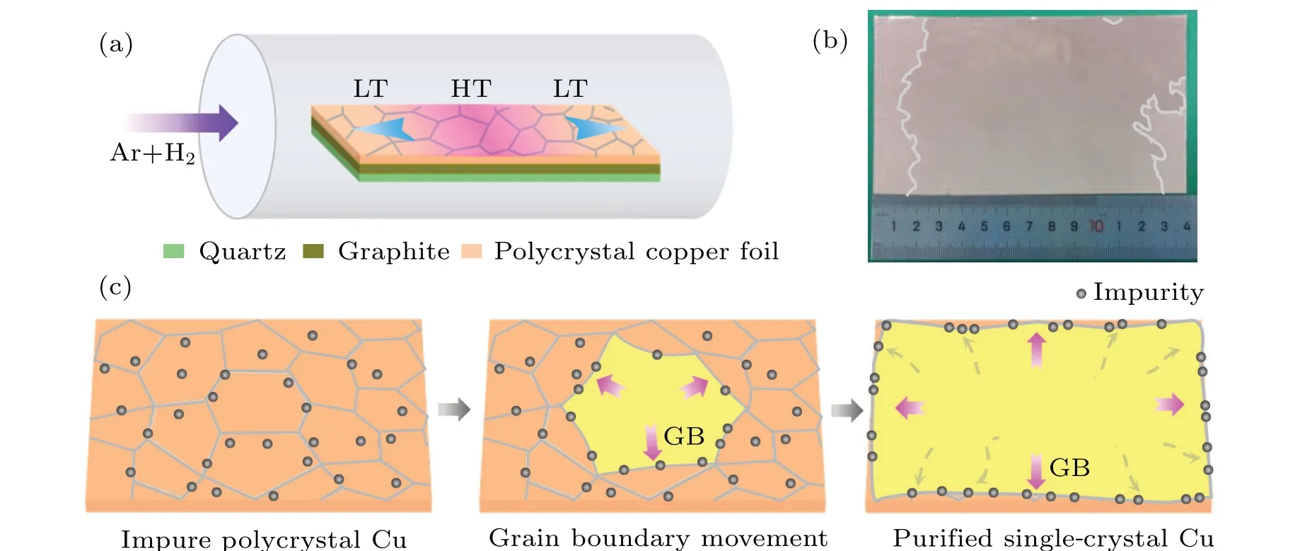
Fig.1.Segregation of impurities along with Cu grain-boundary movement during the thermal annealing process.(a)Schematic diagram of the purification method, highlighting the subtle temperature gradient across the Cu foil.(b)Optical image of the purified single-crystal Cu(111)foil.(c)Schematics of the impurity segregation process,where impurities initially exhibit a random distribution across the polycrystalline Cu foil,then with the enlargement of domain size and grain boundary movement,impurities tend to gather at grain boundaries and finally anchor on the purified single-crystal Cu localized edges.
To test the change of impurity concentration, we have employed Nano-SIMS under ultra-high vacuum conditions of 10-10Pa.This technique enables us to detect the spatial distribution of elements across the Cu foil before and after the thermal annealing process.Figure 2(a) presents the element distribution prior to annealing, where the characteristic elements S (pink) and Cl (green) exhibit a random dispersion across the surface of the polycrystalline Cu.Their concentrations are approximately 9.0 and 3.4 parts per million(ppm)per unit, respectively.After annealing, a minute trace of S and Cl elements persist within the single-crystal domain regions as shown in Figs.2(b) and 2(c).Contrarily, the grain boundary regions exhibit a pronounced accumulation of S and Cl impurities.Quantitative analysis reveals that over 80% of impurities vanish from the single crystal domain regions,and 60% of the remaining impurities are concentrated in the GB regions.[37,38]These results manifest that the impurities dissolved in the polycrystal Cu would be significantly reduced by the temperature-gradient thermal annealing method,in which the movement of grain boundaries plays a critical role in purifying the Cu effectively.
To elucidate the variation in impurity concentration,GDMS is employed to quantify the metallic and nonmetallic composition in Cu foil.Preceding the characterization process, the surface of the single-crystal Cu foil was methodically cleansed through a sequential treatment involving dilute high-purity nitric acid (alfa, 70%,≥99.999% metals basis)and dilute electronic hydrochloric acid (≥99.99%), following by rinsing with ultrapure deionized water.As depicted in Fig.3(a), compared with the pristine polycrystal Cu, the impurity concentration in single-crystal Cu has been significantly reduced after the thermal annealing process.This pronounced impurity reduction mainly arises from two aspects:(i)the segregation of elements with low effective-distribution coefficient,and(ii)the high-temperature evapouration of elements with high saturated vapour pressure.For the segregation mechanism,impurities are prone to segregation when the equilibrium segregation coefficientk0<1 (k0was defined as the ratio of the equilibrium concentration of the solute impurity in the solid to that in the liquid at the interface).[39]Considering the kinetics of single crystal growth, impurity atoms can be swept along with the grain boundary movement and finally anchored at the single-crystal Cu edges.While for the high-temperature evaporation mechanism, impurities are more likely to be volatilized when the saturated vapour pressure of impurity (Pimp) is much higher than that of the Cu unity(lgPimp–lgPCu>2).[40]For reference, the curve depicting the saturated vapor pressure of elements[41,42]is provided in Fig.S2 and Table S1 in the supplementary materials.
Therefore, certain elements of Na, Mg, S, Cl, Ca, Zn,Se, Sb, Te, Pb, and Bi, which conform to the dual criteria of low segregation coefficient and high saturated vapor pressure(Fig.3(a), left panel), display a tremendous reduction after high-temperature annealing.For instance, the concentrations of S atom dwindle from 9.1 ppm to 0.01 ppm,Cl from 4.5 ppm to 0.02 ppm, Pb (1.8 ppm) and Bi (0.36 ppm) decreased to lower than 1 parts per billion(ppb).Notably,despite P and As satisfying both conditions, their high solid solubilities in Cu renders their purification more challenging.Elements of Al,Si,Ag,and Sn,which solely fulfill the condition of low segregation coefficient, prove challenging to eliminate via boundary movement due to their heightened electron affinity for Cu.[40,43]In addition, a handful of metallic impurities, such as Ni and Fe,do not satisfy the aforementioned conditions and perform high solid solubility[44]and surface energy,[45]consequently yielding a limited impact on the purification process (see Fig.S3 in supplementary materials).In addition to the GDMS analysis, we undertook ICP-MS to verify the reduction in impurity levels.This was achieved by completely dissolving the entire foil in high-purity nitric acid(Fig.3(b)).Calibration standards for elements were employed from several mixed,multi-element stock standards(China United Test& Certification Co., Ltd.).These calibration standard solutions were subsequently adjusted to a final volume of 50 mL using ultrapure deionized water, resulting in diluted concentrations of 0 ppb, 40 ppb, 100 ppb, 160 ppb, 200 ppb, and 300 ppb,respectively.The outcomes of this analysis unequivocally affirm the overarching purification effect, both on the surface and within the interior of the Cu, further confirming the success of the purification process.
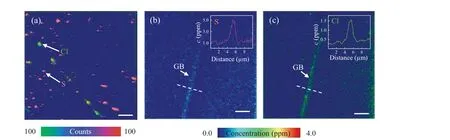
Fig.2.The Nano-SIMS analysis of the variation of impurities.(a)Spatial Nano-SIMS of S(pink)and Cl(green)concentration intensity mapping images of polycrystalline Cu.(b)and(c)Typical Nano-SIMS elemental mappings of S(b)and Cl(c)on the Cu surface around the grain boundary.The inserts are quantitative elemental concentration mapping across the grain boundary marked by the dashed lines.Scale bar,5µm.

Fig.3.Comparison of impurities concentrations between polycrystalline Cu and purified single-crystal Cu foils.(a)GDMS results show that,at 1065 ◦C, thirteen impurity elements such as Na, fulfill both conditions of higher saturated vapor pressure (lgPimp–lgPCu >2) and lower segregation coefficient than that of Cu(left panel).Four impurities such as Al,only fulfill a low segregation coefficient(middle panel).Fe and Ni which fulfill neither of the two conditions are extremely difficult to remove by annealing(right panel).Other impurities are either absent or rare(concentration lower than 0.01 ppm)in polycrystalline Cu.(b)ICP-MS was used to verify the impurity reduction by dissolving the whole foil,which is consistent with the GDMS results.The concentrations shown in unitsµg/L(ppb)in the digest solution are converted into mg/kg(ppm)in the original solid.
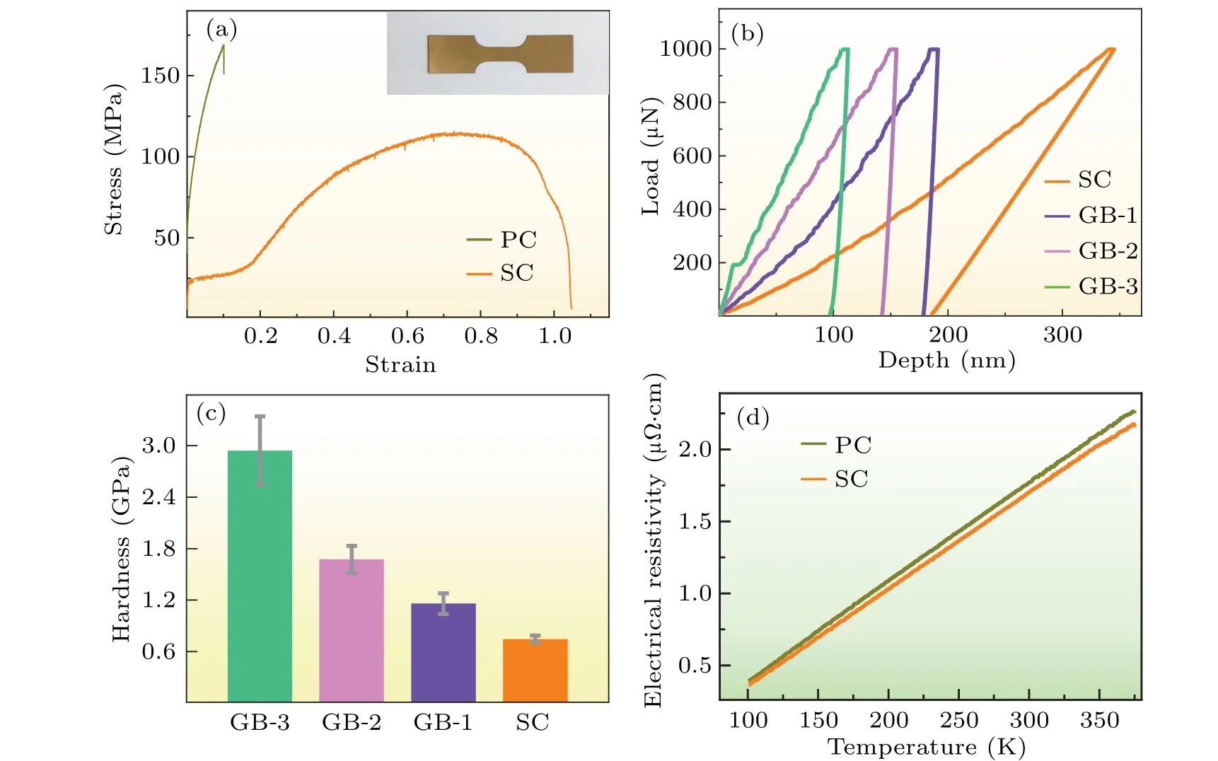
Fig.4.Mechanical and electrical measurements of Cu foils.(a)Tensile stress–strain curves for the purified single-crystal Cu foil and polycrystal counterpart.Inset is the optical micrograph Cu foil.(b)–(c)The hardness evolution for grain boundary regions with domain sizes of 200µm(GB-1),2 mm(GB-2), and 10 cm(GB-3), corresponding to the hardness of 1.16 GPa,1.67 GPa,2.94 GPa,respectively.Here single-crystal Cu(SC)is a control group.(d)The variation trend of electrical resistivity with temperature of polycrystalline Cu and single-crystal Cu foils.
The purified Cu foil showed elevated flexibility and electrical conductivity than that of polycrystalline Cu.The mechanical properties were assessed by an electromechanical universal testing machine (WANCE, TSE504C, with a noncontacting video extensometer)and a nanoindentation system(Bruker’s Hysitron TI 980 TriboIndenter).Prior to conducting the test, all the foil samples (thickness of approximately 25µm)underwent hydrogen annealing at 200◦C for 4 hours to eliminate the ablation edge resulting from laser machining.Subsequently, the tensile tests were performed in alignment with the foil mechanical tensile orientation of〈41 3〉.As shown in Fig.4(a),the stress–strain curve displays a substantial elongation of 70%,which is 7 times that of the commercial polycrystalline Cu foil one(with an elongation of 10%).[46]The superior mechanical flexibility of the purified single-crystal Cu can be attributed to the absence of random defects and deformations between grains,[47]also the purified single-crystal Cu shows lower surface roughness by comparison with the polycrystalline one(see Fig.S4 in supplementary materials).The nanoindentation tests were performed with an applied load of 1000 µN to characterize the hardness within the Cu foil.This examination involved different distinct grain boundary regions,denoted as GB-1,GB-2,and GB-3,with corresponding single-crystal domain sizes of about 200 µm, 2 mm, and 10 cm,respectively.Remarkably,a discernible trend emerged as the crystal domain size expanded, and the grain boundary exhibited a heightened hardness,with the maximum hardness at the grain boundary reaching 2.94 GPa(Figs.4(b)and 4(c)).In comparison,the single-crystal Cu demonstrated a minimum hardness value of 0.74 GPa.The rationale behind this hardness variation lies in the growing propensity of impurities to segregate within boundary regions as larger domains crystallize.In contrast, single crystal regions experience an obvious reduction in hardness,attributed to a decrease in impurity concentration within the domain.These mechanical measurement results demonstrate our hypothesis of impurity migration along with boundary movements.Additionally,we employed the four-probe method to characterize the electrical conductivity of purified Cu foil.The electrical resistivity of polycrystalline and single-crystal Cu was measured to be 1.74µΩ·cm and 1.66µΩ·cm at 293 K,respectively(Fig.4(d)).This difference signifies an enhancement in the electrical conductivity of single-crystal Cu,escalating from 100%IACS to 104%IACS.
4.Conclusion
In summary, we have successfully developed a simple purification technique for Cu foils through a temperaturegradient thermal annealing process.This approach facilitates the transformation from a polycrystalline to a single-crystal state,resulting in an enhanced purity of Cu foil from 3N to 4N.The pivotal mechanisms of impurity reduction involve segregating elements driven by Cu grain-boundary movements and high-temperature evaporation.These processes contribute to the substantial removal of impurities, thereby fine-tuning the flexibility and electrical performance of the Cu foil.Our work has the potential to create new opportunities for the fabrication of high-purity metal foils and will propel the exploration of high-performance device applications within the realm of precision electronic products and high-frequency printed circuit boards.
Acknowledgements
Project supported by the Basic and Applied Basic Research Foundation of Guangdong Province, China (Grant Nos.2019A1515110302 and 2022A1515140003), the Key Research and Development Program of Guangdong Province,China (Grant Nos.2020B010189001, 2021B0301030002,2019B010931001, and 2018B030327001), the National Natural Science Foundation of China (Grant Nos.52172035, 52025023, 52322205, 51991342, 52021006,51991344, 52100115, 11888101, 92163206, 12104018,and 12274456), the National Key Research and Development Program of China (Grant Nos.2021YFB3200303,2022YFA1405600, 2018YFA0703700, 2021YFA1400201,and 2021YFA1400502), the Strategic Priority Research Program of the Chinese Academy of Sciences (Grant No.XDB33000000), the Pearl River Talent Recruitment Program of Guangdong Province, China (Grant No.2019ZT08C321), China Postdoctoral Science Foundation (Grant Nos.2020T130022 and 2020M680178), and the Science and Technology Plan Project of Liaoning Province,China(Grant No.2021JH2/10100012).
杂志排行
Chinese Physics B的其它文章
- Unconventional photon blockade in the two-photon Jaynes–Cummings model with two-frequency cavity drivings and atom driving
- Effective dynamics for a spin-1/2 particle constrained to a curved layer with inhomogeneous thickness
- Genuine entanglement under squeezed generalized amplitude damping channels with memory
- Quantum algorithm for minimum dominating set problem with circuit design
- Protected simultaneous quantum remote state preparation scheme by weak and reversal measurements in noisy environments
- Gray code based gradient-free optimization algorithm for parameterized quantum circuit