5G Wideband Bandpass Filtering Power Amplifiers Based on a Bandwidth-Extended Bandpass Matching Network
2023-11-18WeiminWangHongminZhaoYongleWuXiaopanChen
Weimin Wang ,Hongmin Zhao ,Yongle Wu ,Xiaopan Chen
1 School of Electronic Engineering,Beijing University of Posts and Telecommunications,Beijing 100876,China
2 School of Integrated Circuits,Beijing University of Posts and Telecommunications,Beijing 100876,China
*The corresponding author,email: wuyongle138@gmail.com
Abstract: In this paper,a 5G wideband power amplifier (PA) with bandpass filtering response is synthesized using a bandwidth-extended bandpass filter as the matching network (MN).In this structure,the bandwidth(θC)is defined as a variable in the closedform equations provided by the microstrip bandpass filter.It can be extended over a wide range only by changing the characteristic impedances of the structure.Different from the other wideband MNs,the extension of bandwidth does not increase the complexity of the structure(order n is fixed).In addition,based on the bandwidth-extended structure,the wideband design of bandpass filtering PA is not limited to the fixed bandwidth of the specific filter structure.The theoretical analysis of the MN and the design flow of the PA are provided in this design.The fabricated bandpass filtering PA can support almost one-octave bandwidth (2-3.8 GHz),covering the two 5G bands (n41 and n78).The drain efficiency of 47%-60%and output power higher than 40 dBm are measured.Good frequency selectivity in S-parameter measurements can be observed.
Keywords: bandpass filtering;bandwidth-extension;fixed order;power amplifier;wideband
I.INTRODUCTION
With the development of wireless communication,wideband radio frequency (RF) systems are in high demand to cover not only the bandwidth of the highspeed signal but also multiple frequency bands.At present,5G technology brings higher-speed signals and richer frequency bands[1,2].This means that the design of the RF system requires the further extension of bandwidth.In addition,the higher frequency of the 5G signal will result in greater transmission loss.This means that the power consumption of the RF system will increase[3].In this case,the efficiency enhancement of RF system is also crucial.As one of the most power-consuming components in the RF system [4],wideband high-efficiency PA has become the design goal of researchers and engineers.It is well known that PA performance is the best when conjugate impedance matching is achieved at both source and load ends of the transistor.Therefore,the bandwidth extension of the PA essentially requires impedance matching at more frequency points.For extending bandwidth,some wideband matching networks are studied[5–7].In[8],a synthesized three-stage lowpass matching network is utilized to design a 0.9-2.2 GHz class-E PA with drain efficiency(DE)of 63%-89%.Based on the broadband impedance transformer optimized by the simplified real frequency technique (SRFT),a PA is designed to support 0.9-2.8 GHz [9].To further enhance efficiency,harmonic-control theories are proposed,such as class-F and class-F-1[10,11].By controlling the 2nd harmonic short and the 3rd harmonic open,a class-F PA is implemented in[12].The power added efficiency(PAE)of 85%at 2 GHz is achieved.But in wideband PA design,it is difficult to keep the harmonics open/short in multiple frequency points simultaneously.To solve this problem,the continuous mode theories are proposed such as continuous class-F [13] and class-J [14].By expanding the harmonic design space,a continuous class-F wideband highefficiency PA is proposed in [15],with DE of 70%-83%at 1.15-2.2 GHz.
In order to achieve the system miniaturization,the co-designs of multiple RF components are studied such as the designs of filtering balun and filtering PA[16–22].The co-designs can not only reduce the circuit size,but also reduce the transmission loss and signal reflection caused by the mismatch between RF components.In[20],a compact bandpass filtering PA with the PAE up to 69.8%at 2.1-2.7 GHz is proposed,using two symmetric open-loop resonators as the output matching network (OMN).Based on a D/CRLH bandpass filtering matching topology,a 1.25-2.4 GHz bandpass PA is presented in[21].In[22],coupled microstrip line structure is used as the MN,which shows a good frequency response.However,the aforementioned filtering PAs cannot achieve further bandwidth extension,because their specific filtering MNs cannot expand bandwidth by changing circuit parameters.The reason behind this is that the theoretical closedform design equations including the bandwidth variable cannot be obtained from these filtering MNs.In such a context,the wideband design of filtering PA becomes not flexible enough to meet the practical requirements.Therefore,it is necessary to provide a design demonstration of filtering PA with bandwidth extension.
This paper proposes a wideband bandpass filtering PA based on a microstrip bandpass filter with opencircuited parallel stubs.This structure can expand the bandwidth freely only by changing the characteristic impedances of the microstrip lines.The complete design closed-form equations including bandwidth (θC)variable are provided.To maintain high efficiency in the operating frequencies,the electrical lengths of all the microstrip lines are tuned to keep the harmonic impedances away from the efficiency drop regions.For further proving the feasibility and flexibility of the bandwidth-extended design,the presented wideband bandpass filtering PA is fabricated and measured.Based on the design synthesis,the bandwidth of the filtering PA can be further extended according to the demands.
II.WIDEBAND BANDPASS FILTERING PA DESIGN
As shown in Figure 1,the complete circuit of the wideband bandpass filtering PA consists of a transistor,a bias network,a stabilizing network,and bandwidthextended bandpass filtering MNs.The GaN HEMT transistor CGH40010F from Cree is selected,which can offer high efficiency and high gain across 0.1-6 GHz.In the bias network,the traditional quarterwavelength bias line is replaced by a compact wideband RF choke 4310LC from Coilcraft.The chokecan provide RF blocking and DC feed over a wider bandwidth.The drain voltage and quiescent current are set toVD=28 V andIDQ=210 mA,according to the results of DC sweeping by Advanced Design System (ADS) software.In addition,in-band stability is mainly guaranteed by the parallel RC network.Considering the influence of parasitic parameters,the parasitic equivalent circuit of the transistor package is added to the output during the design process [23].In the following Subsections 2.1-2.3,the designs of the bandwidth-extended bandpass MN and PA are described in detail.
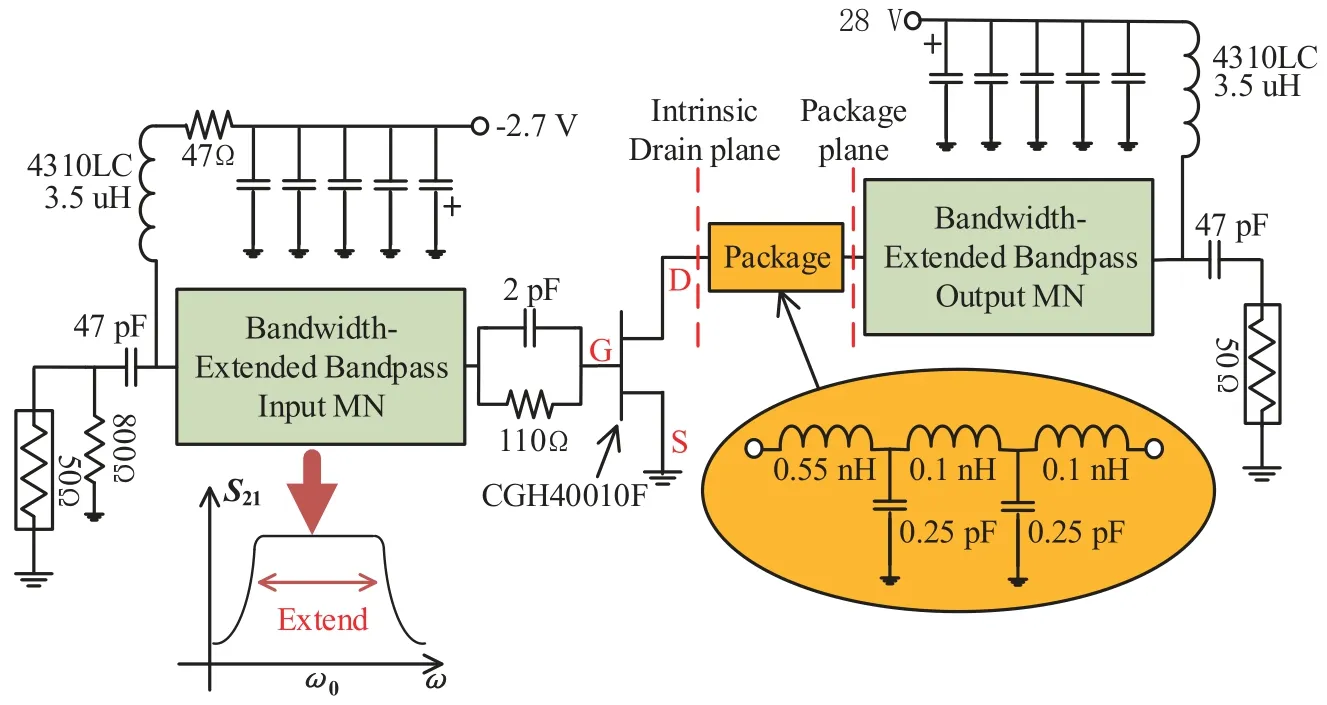
Figure 1. Topology of the proposed wideband bandpass filtering PA.
2.1 Synthesis of the Bandwidth-Extended Bandpass MN
The bandpass filter with the bandwidth-extended function is designed into the MN of the PA,as shown in Figure 2.Compared to the other complex bandpass MNs,the symmetrical microstrip structure is composed of 4-section cascaded transmission lines (TLs)and two short-circuited parallel stubs.The electrical lengths of all these microstrip lines are set to quarterwavelength at the center frequency(f0).More importantly,their characteristic impedances can be directly calculated by the design closed-form equations,according to the desired bandwidth (θC).This provides more freedom for the wideband design of filtering PA,compared to the other specific filtering MNs.Besides,different from the other wideband MNs such as the lowpass MN[24],the circuit complexity does not increase with the bandwidth extension.The complete ABCD matrix elements of the topology can be expressed as follows[25]:
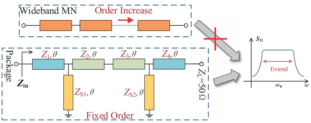
Figure 2. Topology of the bandwidth-extended bandpass filter(order n=4).[25]
whereai,bi,ci,anddiare polynomials containing the characteristic impedances of TLs and parallel stubs,which are described in [25].Then,theS-parameters of the two-port symmetrical lossless structure can be derived as[25]:
whereZLis the load impedance of this structure.It is assumed thatZin/ZL=kis the impedancetransforming ratio.Then,Eq.(3)can be obtained from[25].
wherem=0,2,4,n=1,3,5,andFStructureis the characteristic function of this topology.Based on the synthesis approach in[26],the theoretical Chebyshev transfer function can be expressed as follows:
whereεis the in-band equal ripple factor.Thel1,l3,andl5are polynomials containing theθC(θCrepresents the bandwidth of this topology).For this topology to achieve the same Chebyshev response,the following equation needs to be established:
Substituting Eq.(3b) and Eq.(4b) into Eq.(5),the equation turns into a system of equations[25]:
Based on the above closed-form Eq.(1)-Eq.(6),the variable bandwidthθCcan be changed as needed.For demonstration,theS-parameters versus bandwidthθCunder the condition ofk=Zin/ZL=35 Ω/50 Ω=0.7 are illustrated in Figure 3.The corresponding characteristic impedances can be obtained in Table 1.It can be found that the bandwidth can be extended from one to more than two octaves,just by changing the characteristic impedances of the topology.Besides,the input impedance within the operational bandwidth can also be changed as you want.It provides a good initial condition for the impedance matching in the wideband PA design.Similarly,for verification,the calculated characteristic impedances of TLs and stubs with different input impedancesZinat the fixedZL=50 Ω are shown in Table 2.
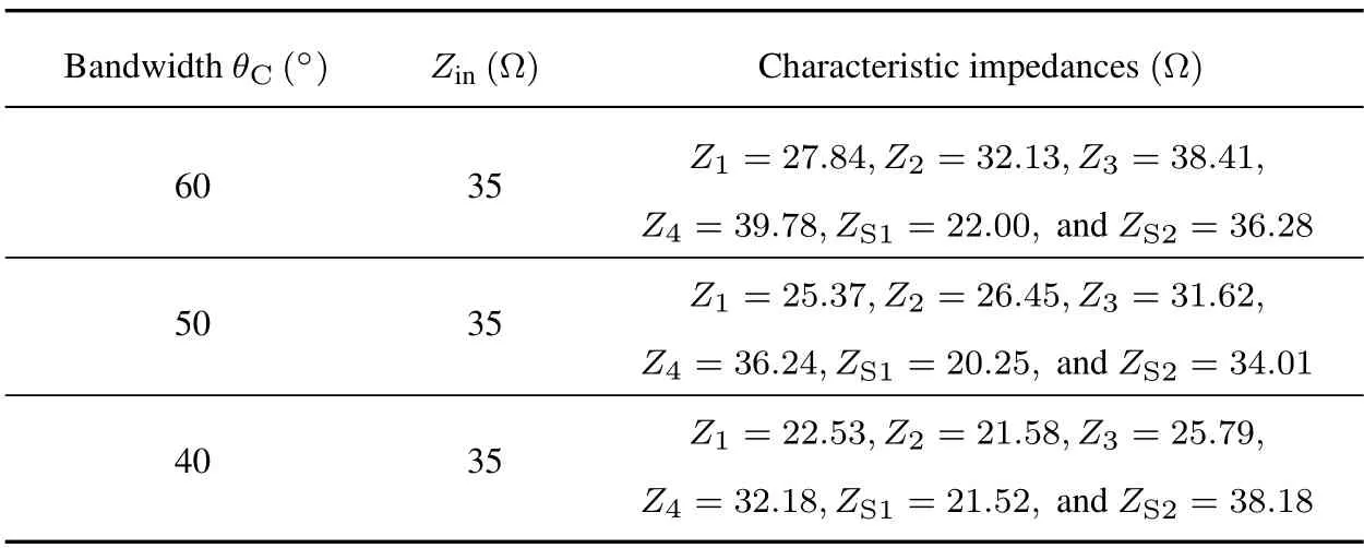
Table 1. The corresponding characteristic impedances with different bandwidth(k=0.7).
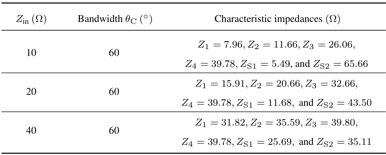
Table 2. The corresponding characteristic impedances with different ZIN(ZL=50Ω).
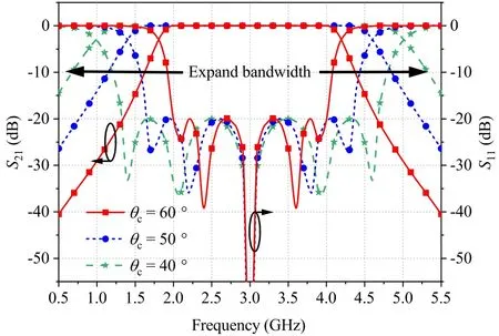
Figure 3. The S-parameters of the 4-order bandpass filter with different bandwidth(k=0.7).
2.2 Analysis of the High Efficiency Region by Load-pull
Note that the bandwidth can be extended to more than one octave.To maintain high efficiency at the extended bandwidth,the harmonic control of the transistor output is needed,especially for the second harmonic.However,it is difficult to achieve precise harmonic control in such a wide bandwidth.In particular,when the bandwidth is close to or even more than one octave,the second harmonic of low operating frequency will close to or overlap with the high operating frequency,which will lead to a contradiction between the second harmonic and the fundamental matching.
In this situation,it is necessary to expand the design space of the second harmonic.By sweeping the phase of the second harmonic reflection coefficient in ADS[27],it is noticed that there is an efficiency drop region in the second harmonic.When the second harmonic does not approach the drop region,its effect on efficiency is almost negligible.This makes it easier to keep high efficiency in an extended bandwidth,without the need for precise second harmonic control.As shown in Figure 4,the second harmonic phase of the CGH40010F is swept at 2.5,3.0,and 3.5 GHz by loadpull simulations.Similarly,all the second harmonics at different frequency points exist in efficiency drop regions.In the following Subsection 2.3,this method is adopted to keep high efficiency in bandwidth-extended filtering PA design.
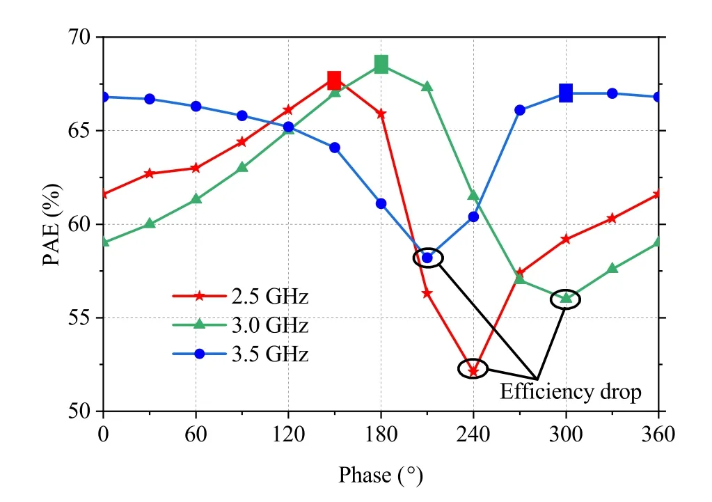
Figure 4. Simulated PAE by sweeping the phase of the second harmonic(ZL,f0=21.4+j*3.4Ω).
2.3 PA Design and Implementation
Herein,the one octave wideband bandpass filtering PA is designed,using the bandwidth-extended bandpass MN.Since the existence of the DC bias circuit in PA,the short-circuitλ/4 stubs of the bandpass MN are replaced by the electrically equivalent open-circuitedλ/2 stubs,as shown in Figure 5.
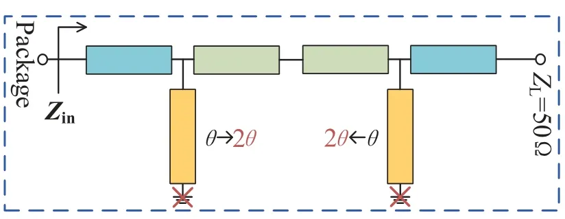
Figure 5. Equivalent substitution of the stubs.
The 2-4 GHz is selected as the target band.It covers the two 5G bands of n41 and n78.In addition,the signals outside the band need to be filtered out.Through source/load-pull simulations,the source/load contours for the PAE at 2.5,3.0,and 3.5 GHz are depicted in Figure 6.The corresponding second harmonic efficiency drop regions(PAE<60%)at these frequencies is also obtained in Figure 7.Through the analysis of the simulated results,the optimal fundamental source impedanceZS,f0and load impedanceZL,f0atf0=3 GHz are set to (10-j*12) Ω and (21.4+j*3.4) Ω.The bandwidth-extended bandpass IMN and OMN are designed in the following,according to the target bandwidth.
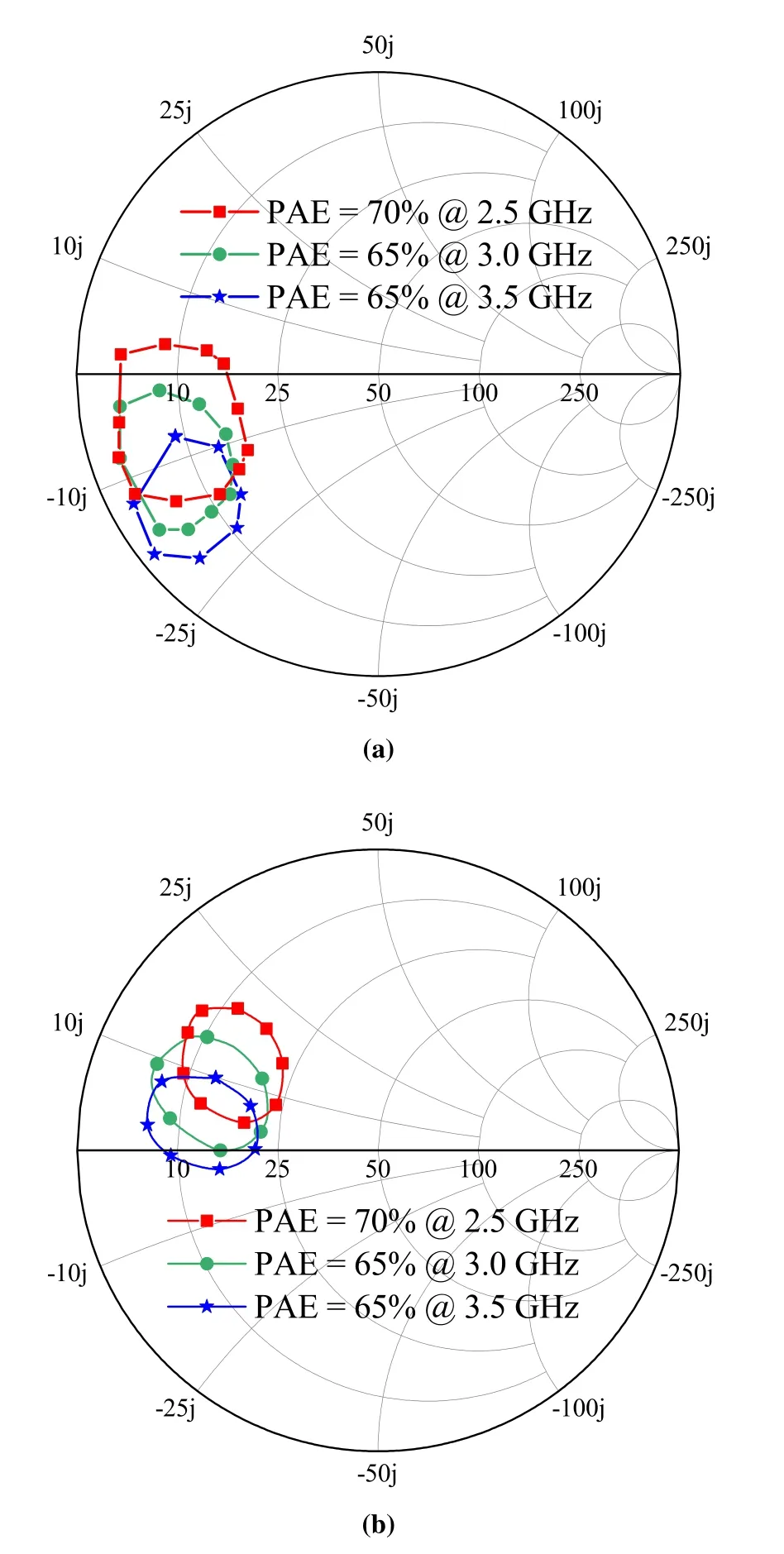
Figure 6. The(a)source and(b)load contours for the PAE at 2.5,3.0,and 3.5 GHz.
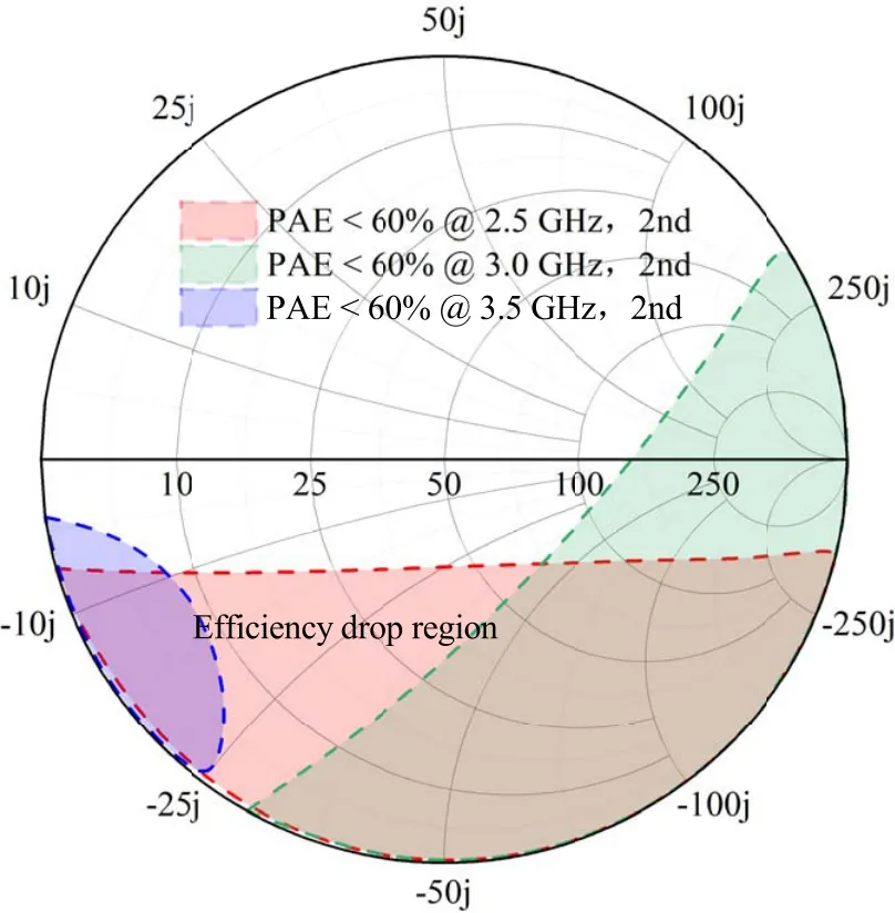
Figure 7. The second harmonic efficiency drop regions(PAE<60%)at 2.5,3.0,and 3.5 GHz.
According to the selected band(2-4 GHz),the center frequencyf0and bandwidthθCof the bandwidthextended bandpass filter are set to 3 GHz and 60°.Besides,the input impedance of this topology is set to 20 Ω (near the optimal load impedanceZL,f0=(21.4 +j*3.4)Ω).Based on the design synthesis provided by Subsection 2.1,the characteristic impedances of this topology are calculated as:Z1=15.91 Ω,Z2=20.66 Ω,Z3=32.66 Ω,Z4=39.78 Ω,ZS1=11.68 Ω,andZS2=43.50 Ω.Then,the short-circuited stubs are replaced with the electrical equivalent open-circuited ones.Finally,for achieving fundamental and second harmonic matching across the operating band,the initial OMN is tuned,as shown in Figure 8.The correspondingS-parameters and the input impedancesZinof the final output MN are presented in Figure 9,respectively.And the second harmonic impedance trajectory is depicted in Figure 10.These results show that the designed bandpass OMN has a good wideband matching and an excellent filtering characteristic.
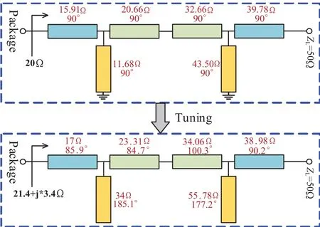
Figure 8. The designed one-octave wideband bandpass OMN.
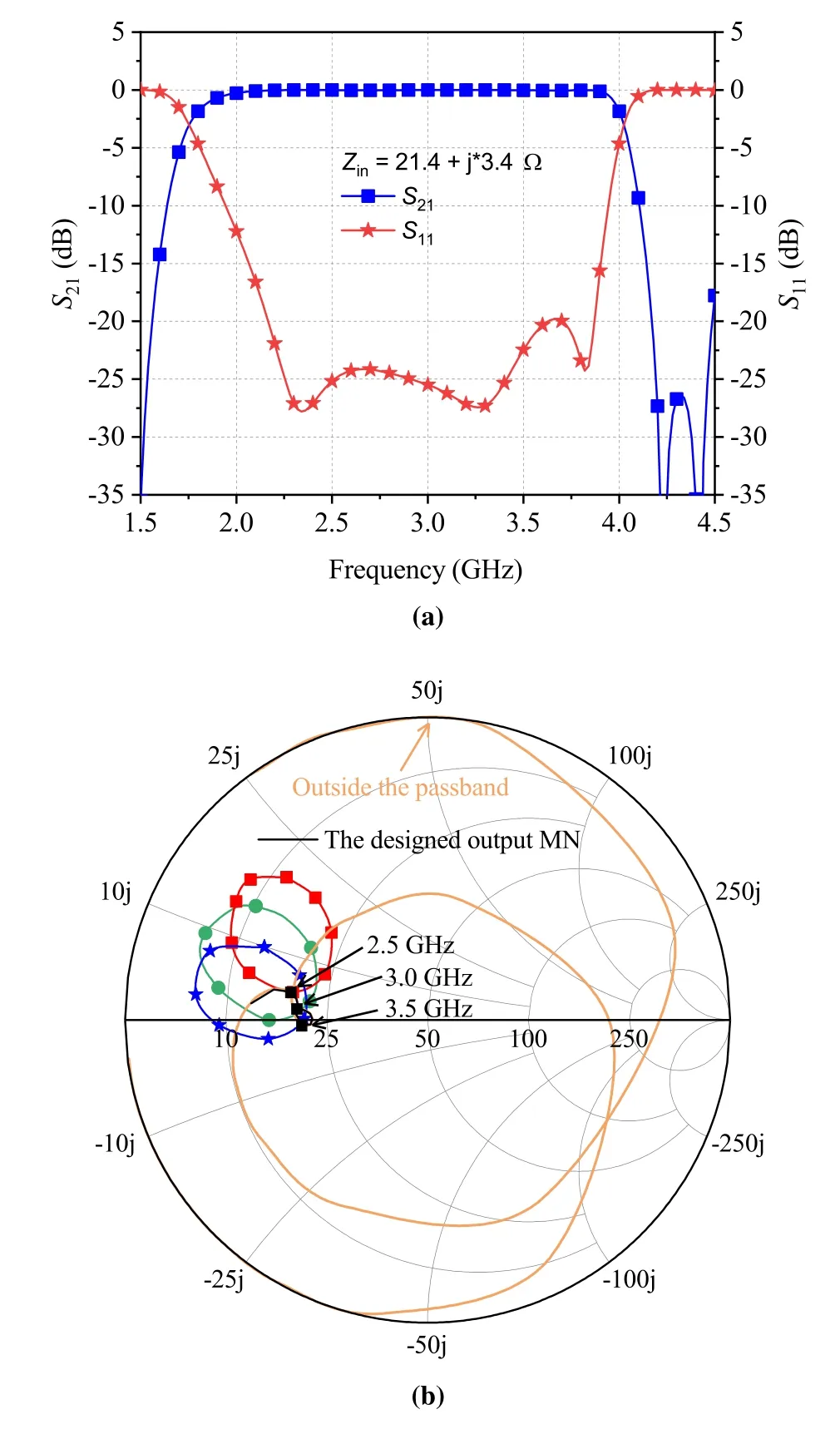
Figure 9. The(a)S-parameters and(b)Zin of the OMN.
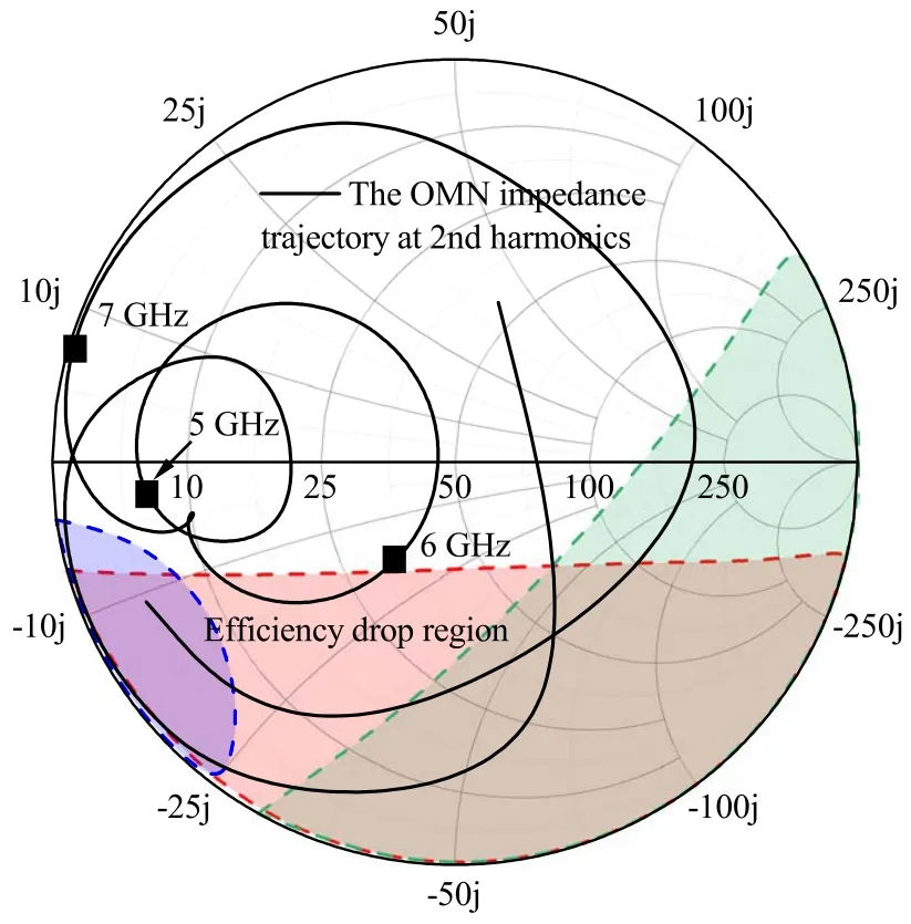
Figure 10. The second harmonic impedance trajectory of the designed OMN.
In the IMN design,harmonic control is not required.Similarly,thef0andθCare 3 GHz and 60°.The input impedanceZinis selected to 35 Ω.Then,two additional tuning lines are added to match the optimal source impedanceZS,f0=(10-j*12) Ω.Finally,after tuning,the circuit parameters of the IMN are obtained in Figure 11.Accordingly,theS11andZinof the final IMN are presented in Figure 12.

Figure 11. The designed one-octave wideband bandpass IMN.
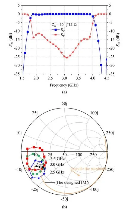
Figure 12. The(a)S-parameters and(b)Zin of the IMN.
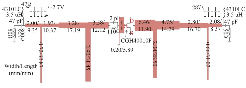
Figure 13. The EM layout with the main physical dimensions and model numbers.
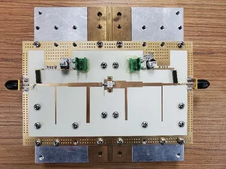
Figure 14. The fabricated photograph of the proposed wideband bandpass PA.
Based on the above design,a 2-3.8 GHz bandpass filtering PA with high efficiency is achieved.The design band failed to reach the target 4 GHz,because the filtering characteristic of the bandpass filtering MN makes the performance at the frequency edge decline rapidly.By tuning,the design band is close to the target one octave bandwidth.For facilitating the understanding,the step-by-step design flow is provided as follows:
Step 1: Set the target operational band;
Step 2:Obtain the PAE contours at the working frequency points,ZS,f0,andZL,f0by source/load-pull;
Step 3: Obtain the second harmonic efficiency drop regions by sweeping the phase;
Step 4: According toZS,f0,ZL,f0,and target band,the input impedanceZinand bandwidthθCof the IMN and OMN are chosen;
Step 5: According to the chosenZinandθCin step 4,calculate the characteristic impedances of the bandwidth-extended filtering MNs by the closed-form Eq.(1)-Eq.(6);
Step 6: Tune the MNs until the in-band matching and out-of-band mismatch are achieved simultaneously;
Step 7: Finally,construct the PA.
III.FABRICATION AND MEASUREMENTS
For further demonstration,the designed PA using a 40-dBm GaN HEMT transistor CGH40010F is EM simulated and fabricated on the RO4350B substrate with a relative permittivity of 3.66,a thickness of 0.762 mm,and a loss tangent of 0.0037.The EM layout and final fabricated PA are shown in Figures 13 and 14,respectively.In the continues wave (CW) signal measurements,the simulated and measuredS-parameters are depicted in Figure 15,which displays a good bandpass filtering response.The return loss is below 10 dB,which meets the default industry standard for high power instruments.Besides,in the large-signal measurements,the measured DE of 47%-60% and gain of 9-10.1 dB are achieved under the saturated output power (Psat) of 40.6-41.7 dBm,as shown in Figure 16.The gain flatness is only ±0.55 dB at 2-3.8 GHz.Moreover,the measured gain and DE versus output power are plotted in Figure 17.Figure 18 shows that the 2ndand 3rdharmonic rejection under the saturated output power are below-16.6 dBc and-17.1 dBc.
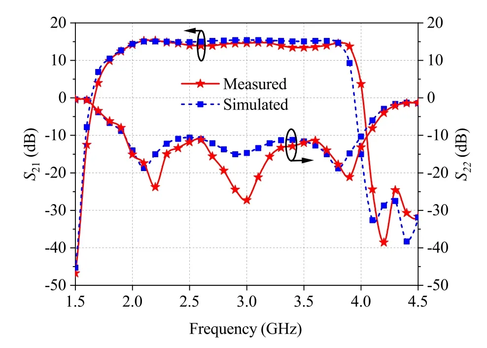
Figure 15. The simulated and measured S-parameters of the designed PA.
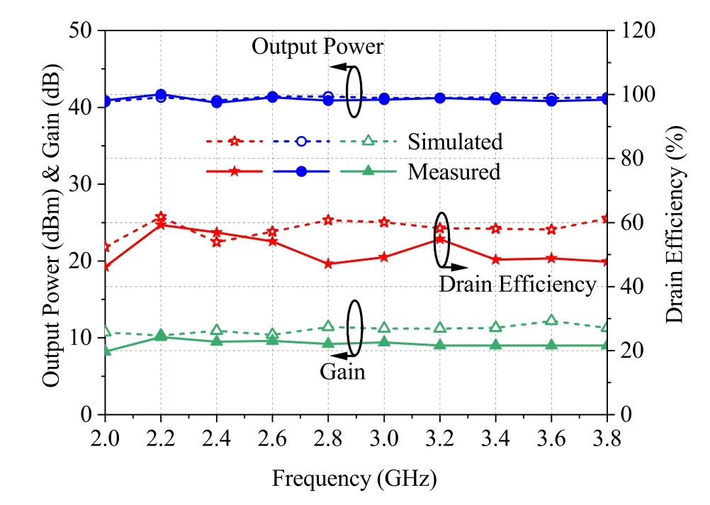
Figure 16.The simulated and measured DE and gain under the saturated output power.
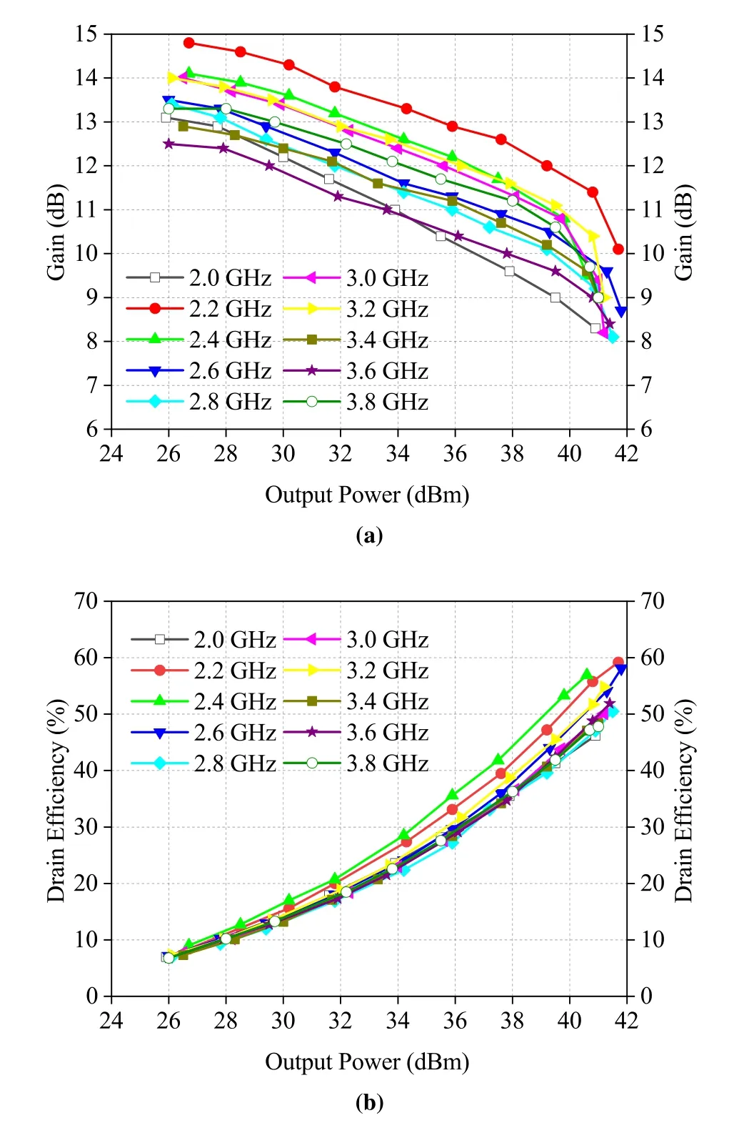
Figure 17.The measured DE and gain versus output power.
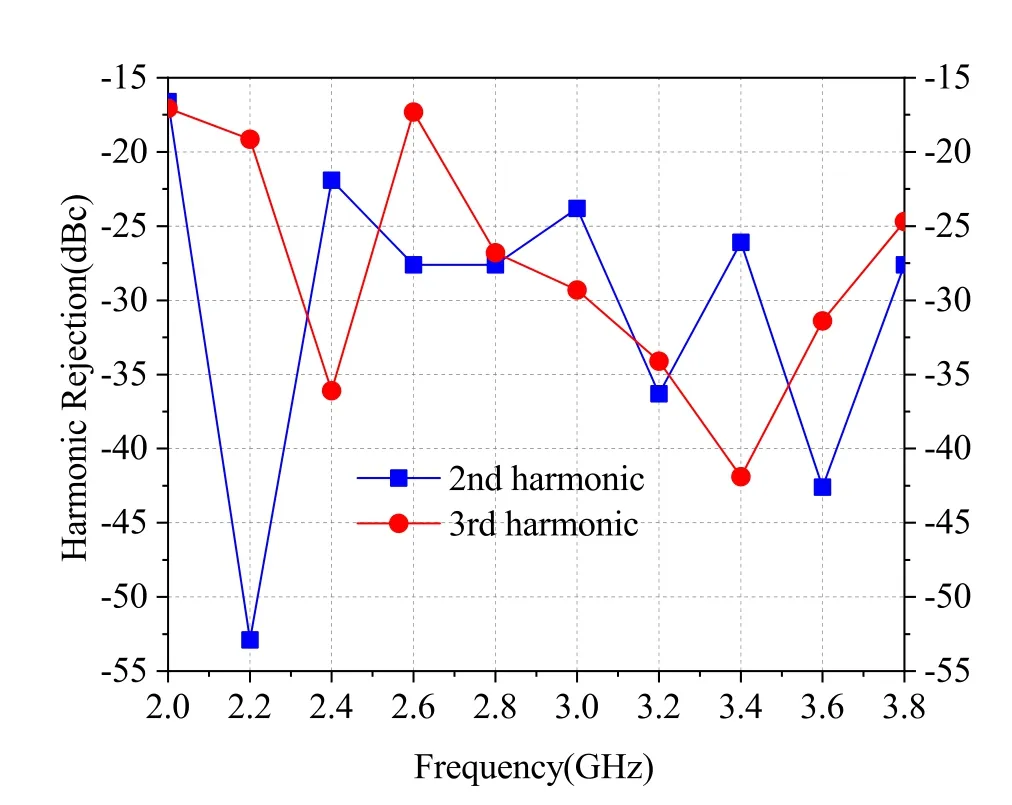
Figure 18. The simulated results of the harmonic components.
Compared with the simulated results,it can be seen that the measured gain and efficiency degrade slightly around 2.8 GHz and 3.5 GHz.This indicates that there are impedance mismatches between the fabricated microstrip circuit and practical transistor at these frequencies.The cause of these mismatches may be: 1)the PCB fabrication errors;2)the simulated model errors including the transistor,capacitors,and resistors.
Table 3 shows the performance comparison of the proposed PA with other previously works.Compared with other wideband PAs,this work displays better frequency selectivity and in-band gain flatness(±0.55 dB).Furthermore,although the efficiency of the other filtering PAs in [20–22] is better than this work,the almost one octave bandwidth(2-3.8 GHz)in this work is wider than ones in[20–22].
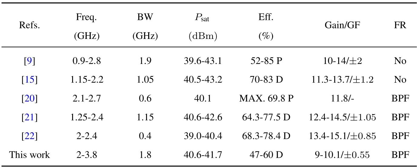
Table 3. Comparison of this work with other PAs using the CGH40010F.
IV.CONCLUSION
In this paper,a fixed order bandpass filter with the function of bandwidth extension is designed as the matching network of the PA.Based on this structure,the bandwidth of the filtering PA can be extended to one octave above according to the design demands.It provides more freedom for the wideband filtering PA design.The complete synthesis of the MN and design procedure of the PA are provided step-by-step.A design example of the proposed PA is fabricated for demonstration.The measured results show that the bandpass filtering PA has a 1.8-GHz working frequency range (2-3.8 GHz) with only ±0.55-dB gain flatness.
ACKNOWLEDGEMENT
This work was supported by National Natural Science Foundations of China (No.61971052 and No.U20A20203) and Key Research and Development Project of Guangdong Province(2020B0101080001).Mr.H.Zhao’s Master’s Dissertation in 2022 includes this paper as chapters.(Corresponding author: Yongle Wu).
杂志排行
China Communications的其它文章
- Secure and Trusted Interoperability Scheme of Heterogeneous Blockchains Platform in IoT Networks
- Intelligent Edge Network Routing Architecture with Blockchain for the IoT
- Privacy-Preserving Deep Learning on Big Data in Cloud
- PowerDetector: Malicious PowerShell Script Family Classification Based on Multi-Modal Semantic Fusion and Deep Learning
- Dynamic Task Offloading for Digital Twin-Empowered Mobile Edge Computing via Deep Reinforcement Learning
- Resource Trading and Miner Competition in Wireless Blockchain Networks with Edge Computing
