Influence of deposition power on the optical and electrical performance of sputtered gallium-magnesium co-doped zinc oxide thin films
2023-11-07ZHONGZhiyouWANXinGUJinghuaLONGHaoYANGChunyongCHENShoubu
ZHONG Zhiyou,WAN Xin,GU Jinghua,LONG Hao,YANG Chunyong,CHEN Shoubu
(1 College of Electronic Information Engineering,South-Central Minzu University,Wuhan 430074,China;2 Hubei Key Laboratory of Intelligent Wireless Communications,South-Central Minzu University,Wuhan 430074,China;3 Experimental Teaching and Engineerring Training Center,South-CentralMinzu University,Wuhan 430074,China)
Abstract The transparent conductor thin films of gallium-magnesium co-doped zinc oxide(ZnO:Ga-Mg)were deposited by magnetron-sputtering process.The deposition power dependence of structural,morphological,optical and electrical properties of the thin film was characterized by various techniques.The experimental results indicate that all the thin films have hexagonal wurtzite structure with highly c-axis preferred orientation along the(002)plane,and the deposition power strongly affects the properties of ZnO:Ga-Mg thin films.The thin film prepared at the deposition power of 150 W exhibits the best crystallinity quality and photoelectric properties,with the highest average visible transmittance of 92.2%,the lowest resistivity of 1.18×10⁻³ Ω·cm,the maximum figure of merit of 1.04×10⁴ Ω-1·cm-1,and the minimum lattice strain of 1.95×10⁻³ and dislocation density of 1.17×10¹⁵ m-2.The optical constants of the thin films were obtained by the optical characterization methods.The optical dispersion behavior of the thin films was studied in terms of the single-oscillator Wemple-DiDomenico(WDD)model,and the oscillator parameters,non-linear optical constants and optical energy-gaps were achieved.The results demonstrate that the deposition power is one of the most important processing parameters to affect the structure,optical and electrical properties of ZnO:Ga-Mg thin films.
Keywords ZnO;thin films;doping;photoelectric properties
Gallium-doped zinc oxide(ZnO:Ga)is a promising transparent conductor material which has numerous applications in modern technologies such as organic light emitting diodes(OLEDs)[1-2],flat panel displays(FPDs)[3-4],thin film transistors(TFTs)[5-6],photovoltaic cells(PVCs)[7-8],gas sensitive devices[9-10]and ultraviolet(UV)photodetectors[11-13].Besides good electrical conductivity and high visible light transparency,the ZnO:Ga thin films have a variety of advantages,such as material abundance,non-toxicity,low manufacture cost,high exciton binding energy(about 60 meV at room temperature),broad direct energy-gap(about 3.3 eV at room temperature)and excellent chemical-stability under hydrogen plasma,as compared to the tin-doped indium oxide(In2O3:Sn)thin films[14-17].In order to further improve the optical and electrical properties of ZnO:Ga thin films,the codoping process with two elements have been used.Up to now,the titanium-gallium(Ti-Ga),aluminumgallium(Al-Ga),gallium-zirconium(Ga-Zr),galliumindium(Ga-In),boron-gallium(B-Ga),galliumfluorine(Ga-F),magnesium-gallium(Mg-Ga)and nickel-gallium(Ni-Ga)co-doping cases have been reported[18-27].However,few reports have been devoted to the non-linear optical properties and optical dispersion behavior of the co-doped ZnO thin films.
In this work,the Ga-Mg co-doped ZnO(ZnO:Ga-Mg)thin films were prepared by radio-frequency(RF)magnetron-sputtering process under various deposition powers.The dependence of structure,morphology,photoelectric and non-linear optical properties of the thin films on power was investigated in detail.In addition,the optical constants of the thin films were obtained using the optical characterization methods,and the optical dispersion behavior was studied in terms of the single-oscillator Wemple-DiDomenico(WDD)model.
1 Experimental
A quartz glass was employed as the transparent substrate,and a ceramic target(ZnO:95 wt%,Ga2O3:3 wt%,MgO:2 wt%,4N in purity)was used as the sputtering source material.The ZnO:Ga-Mg samples were prepared on the quartz glass substrates by RF magnetron-sputtering system(13.56 MHz).The base pressure in deposition chamber was kept blow 2.25×10⁻⁴Pa and high purity argon gas(5N in purity)was used as the working gas.Prior to the ZnO:Ga-Mg samples deposition,the pre-sputtering for 20 min was conducted in order to clean contamination on the ceramic target surface.The ZnO:Ga-Mg samples were prepared under the following processing parameters:7.5 cm of target-substrate distance,300 ℃ of substrate temperature,3.5 Pa of gas pressure and 40 min of sputtering time.In order to investigate the effect of deposition power on the properties of ZnO:Ga-Mg thin films,the power was controlled from 110 to 170 W.
The thickness of the ZnO:Ga-Mg thin films was measured by an Alpha-step 500 type surface profiler.The surface morphology of the thin films was observed by a JSM-6700F type scanning electron microscope(SEM).The electrical properties of the thin films were investigated at room temperature using a RH-2035 type four-point probe measurement system.The X-ray diffraction(XRD)patterns of the thin films were characterized with a D8-Advanced type diffractometer using standard Cu Kα source(wavelengthλ=0.15406 nm).The optical transmittance(T)of the thin films were measured at room temperature by using a TU-1901 type double beam UV-visible spectrophotometer.The optical constants of the ZnO:Ga-Mg thin films were obtained from the measured transmittance data using the method of optical spectrum fitting[28].All measurements were performed in ambient air.
2 Results and discussion
Figure 1 shows the XRD patterns of the standard ZnO powder(PDF 036-1451)and the ZnO:Ga-Mg samples prepared at various powers.From the figure,we note that these XRD peaks of the investigated samples can be assigned to ZnO according to PDF 036-1451 card.All the investigated samples exhibit a dominant(002)peak with slight(101)and(004)peaks,indicating that the ZnO:Ga-Mg thin films have hexagonal wurtzite structure of ZnO with preferredcaxis orientation along the(002)plane,regardless of power.Also,no diffraction peaks from other impurities can be detected from Figure 1,which indicates that all the ZnO:Ga-Mg thin films in this work do not have any phase segregation or secondary phase formation.Similar results have been reported by other researchers who investigated the structural properties of ZnObased thin films[18,21,29-30].

图1 PDF 036-1451和不同功率时所制备薄膜的XRD图谱Fig.1 XRD patterns of PDF 036-1451 and the thin films prepared at various powers
The intensity of(002)diffraction peak(I(002))for the ZnO:Ga-Mg samples as a function of power is shown in Figure 2a.As can be seen,the value ofI(002)rises first and thereafter drops with the increment of power.The ZnO:Ga-Mg thin film deposited at the power of 150 W presents the highest intensity of(002)diffraction peak.The degree of preferred(002)orientation of the ZnO:Ga-Mg thin films was quantified by means of the orientation factor(P(002))[31]:

图2 不同功率时所制备薄膜的I(002)和P(002)数值Fig.2 The values of I(002) and P(002) for the thin films prepared at various powers
whereI(002)is the intensity of(002)diffraction peak,the subscripth,kandlare Miller indices,I(hkl)denotes the diffraction intensity of the(hkl)plane,andNis the number of the diffraction peaks.Figure 2b shows the variation ofP(002)with power for the ZnO:Ga-Mg thin films.It is found that with increasing power from 110 to 170 W,theP(002)value raises first and subsequently falls.When the power is 150 W,the maximumP(002)value can be obtained,indicating that the ZnO:Ga-Mg sample has the highestc-axis preferred orientation when the power is 150 W.
The mean particle size(Dm)of the ZnO:Ga-Mg samples was evaluated using the Debye-Scherrer formula[31-32]:
whereθis the Bragg’s diffraction angle,βis the fullwidth at half-maximum(FWHM,in radians)of(002)diffraction peak,andλdenotes the wavelength of XRD measurement used(λ=0.15406 nm).The lattice strain(ε0)and the dislocation density(δ0)can be obtained by means of the following relationships[33-34]:
whereDmrepresents the mean particle size,βis the value of FWHM in radians,θdenotes the Bragg’s angle,andλis the wavelength of X-ray used.Figure 3 shows the variation in theβ,Dm,ε0andδ0values of the investigated thin films as a function of power.It can be noticed from Figure 3 that with rising power from 110 to 170 W,the values ofβ,ε0andδ0increase in advance and then fall,but theDmtakes on an opposite trend.When the power is 150 W,the ZnO:Ga-Mg thin film exhibits the optimum crystallinity quality and structural properties,with the narrowestβ(4.91×10⁻³rad),the largestDm(29.3 nm),the lowestε0(1.95×10⁻³)and the minimumδ0(1.17×10¹⁵m-2),respectively.This result demonstrates that the grain growth and structural properties of the ZnO:Ga-Mg thin films are subjected to the deposition power.

图3 不同功率时所制备薄膜的β,Dm,ε0和δ0数值Fig.3 The values of β,Dm,ε0 and δ0 for the thin films prepared at various powers
Figure 4 presents the dependence of optical transmittanceTon wavelengthλfor the ZnO:Ga-Mg samples prepared at various powers.As can be seen,all theT-λcurves exhibit an interference pattern where the transmittance falls rapidly at the edge of the bands,which indicates excellent film crystallinity and low surface roughness.Also,the absorption edge is observed to blue shift firstly with the increasing power from 110 to 150 W and then red shift from 150 to 170 W,as shown in the inset of Figure 4.The power dependence of the mean transmittance(Tm)in the visible wavelength range for the ZnO:Ga-Mg samples is presented in Figure 5a.Note that theTmvalue exceeds 85.7% for the investigated samples regardless of power,which indicates that all the ZnO:Ga-Mg thin films possess high transparency in the visible light region.The highest value(92.2%)ofTmfor the ZnO:Ga-Mg sample can be achieved when the power is 150 W.The enhancement of optical transmittance may be caused by the improvement of crystallinity quality and structural properties of the ZnO:Ga-Mg thin film.
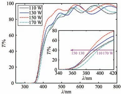
图4 不同功率时所制备薄膜的T-λ曲线Fig.4 The curves of T-λ for the thin films prepared at various powers
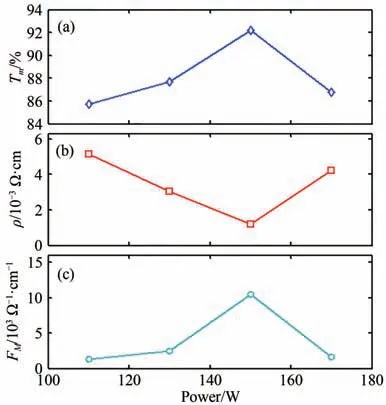
图5 不同功率时所制备薄膜的Tm,ρ和FM数值Fig.5 The values of Tm,ρ and FM for the thin films prepared at various powers
In order to quantify the photoelectric properties of the ZnO:Ga-Mg transparent conductor oxide (TCO)thin films,the figure of merit(FM)was introduced.TheFMis defined by the following relation[35-36]:
whereρdenotes the resistivity of the investigated sample,andTmis the average transmittance in the visible range.The power dependence ofρandFMfor the ZnO:Ga-Mg samples is shown in Figure 5.It is observed from Figure 5b that theρfalls firstly with the rising power from 110 to 150 W and then increases from 150 to 170 W.The minimumρ(1.18×10⁻³Ω·cm)of the ZnO:Ga-Mg sample can be obtained when the power is 150 W.The optimalρvalue in this work is comparable to the results of previous studies.For the ZnO-based thin films deposited by RF-sputtering technique,the lowestρvalues were reported to be ranging from 7.23×10⁻⁴to 1.52×10⁻³Ω·cm[19,37-38].Note also from Figure 5c that theFMvalues are found to be 1.26×103,2.49×103,1.04×104and 1.67×10³Ω-1·cm-1for the ZnO:Ga-Mg samples fabricated at the power of 110,130,150 and 170 W,respectively.Clearly,theFMraises first and subsequently falls with the increment of power,the ZnO:Ga-Mg thin film deposited at the power of 150 W exhibits the maximumFMvalue,indicating that the optimum deposition power is 150 W for preparing ZnO:Ga-Mg thin film in the present work.
The direct optical energy-gap()of the ZnO:Ga-Mg thin films was evaluated by using the Tauc’s relation in the region of high absorption[39-40]:
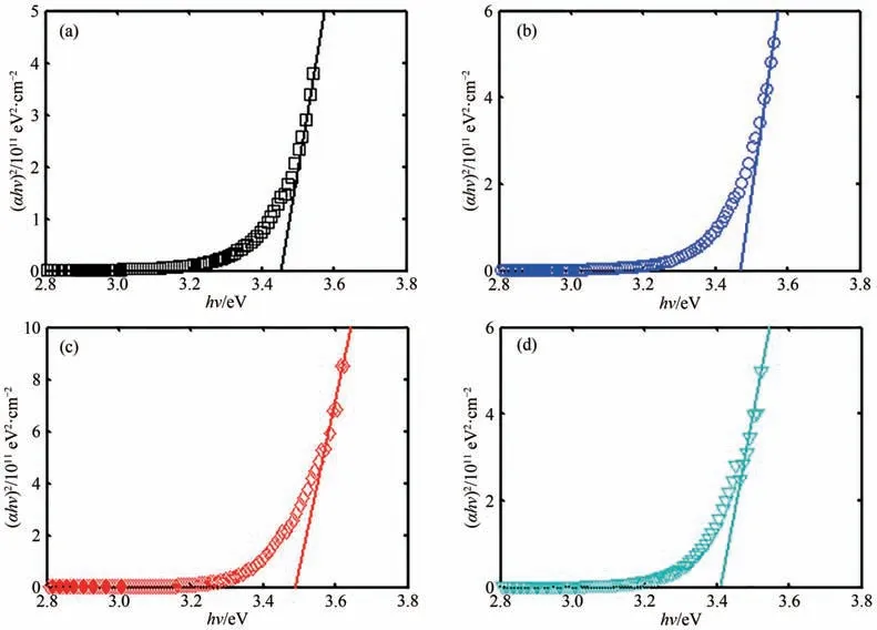
图6 不同功率时所制备薄膜的(αhν)2-hν曲线Fig.6 The curves of(αhν)2-hν for the thin films prepared at various powers
wherehis Planck’s constant,νis the photon frequency,Bis an energy-independent constant,tfis the film thickness,andαis the absorption coefficient of the thin film[41-42].Figure 6 shows the (αhν)2vs.hνplots of the ZnO:Ga-Mg samples prepared at various powers.As can be seen,a good straight line can be obtained in the band edge region for all the investigated thin films.The straight-line portion of the curve gives the direct optical energy-gapwhen extrapolated to zero((αhν)2=0).The values ofare evaluated to be ranging from 3.41 to 3.49 eV for the ZnO:Ga-Mg samples prepared at various powers.Obviously,the obtainedvalues of all the ZnO:Ga-Mg thin films are larger than that of standard ZnO sample(3.30 eV)[18,43].The broadening inof the ZnO:Ga-Mg thin films mainly be attributed to the Burstein-Moss(B-M)effect[44-47].Similar results have been observed by many researchers who studied the optical properties of ZnObased thin films[47-50].
Based on the measured transmittance,the optical constants including extinction coefficient(k)and refractive index(n)of the ZnO:Ga-Mg thin films were obtained by the method of optical spectrum fitting[28],and the dependence ofkandnonλfor all the samples is shown in Figure 7.It can be seen from Figure 7a that thekvalues of the investigated samples are very small at long wavelength region,which indicates that all the investigated thin films have high visible transparency.Similar to thek-λcurves,thengradually falls with raisingλfor all the ZnO:Ga-Mg samples.The result suggests that all the ZnO:Ga-Mg thin films exhibit the normal dispersion characteristics in the visible wavelength range[31].For the ZnO:Ga-Mg samples deposited at the power of 110,130,150 and 170 W,the values ofkandnare 1.16×10-2,1.87;8.93×10-3,1.96;3.54×10-3,1.91;and 8.45×10-3,1.94 atλ=450 nm,respectively.The result is in agreement with the previously reported works[51-53].
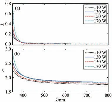
图7 不同功率时所制备薄膜的k-λ和n-λ曲线Fig.7 The curves of k-λ and n-λ for the thin films prepared atvarious powers
The refractive index dispersion behavior of the ZnO:Ga-Mg samples was studied according to the single-oscillator WDD model as follows[54-55]:
whereλis the wavelength of incident light,hdenotes Planck’s constant,cis the light speed,andE,EdandEoare the incident photon energy,the dispersion energy and the single-oscillator energy,respectively.The dependence of (n2-1)-1onE2for the ZnO:Ga-Mg samples prepared at various powers is shown in Figure 8.As can be seen,the data of all the investigated thin films can be fitted into straight lines,indicating that the single-oscillator WDD model is applicable to the ZnO:Ga-Mg samples in this work.TheEdandEoof all the ZnO:Ga-Mg thin films can be deduced from the slopeand intercept(Ed-1Eo)on the vertical axis.The lattice dielectric constant(εL),the static refractive index(n0),theM-1andM-3moments of the optical spectra were obtained using the following equations[56]:
whereEois the single-oscillator energy,andEdis the dispersion energy.Table 1 lists the values ofEd,Eo,n0,εL,M-1andM-3for all the ZnO:Ga-Mg thin films.TheEovalues can be found to range from 6.07 to 6.80 eV,andEdfrom 11.79 to 14.43 eV for the ZnO:Ga-Mg samples deposited at various powers.In compared with theEd,theEochanges in a very narrow range.Also,it is observed from Table 1 that the deposition power significantly affects the optical parameters of the ZnO:Ga-Mg thin films.
The third-order non-linear optical susceptibility(χ(3)),the non-linear refractive index(n2)and the non-linear absorption coefficient(α2)of the ZnO:Ga-Mg thin films can be obtained using the following formulae[57-58]:

表1 不同功率时所制备薄膜的光学参数Tab.1 The optical parameters of the thin films prepared at various powers

图8 不同功率时所制备薄膜的(n2-1)-1-E2曲线Fig.8 The curves of(n2-1)-1-E2 for the thin films prepared at various powers
whereA=1.7×10⁻¹⁰esu is a constant,cis the speed of light,λis the wavelength of incident light,andnis the refractive index of the thin films.Figure 9 shows the variation in theχ(3),n2andα2values of the ZnO:Ga-Mg thin films as a function of power.Note from Figure 9a that theχ(3)raises rapidly withλdecrease until it reaches a maximum value,and it drops slowly withλincrease until it reaches a constant value for higher wavelengths.In addition,the deposition power has a great influence on theχ(3)in the ultraviolet region,and little influence on theχ(3)in the visible and near-infrared range of the investigated thin films.From Figure 9,we can observe that the variation ofn2andα2follow the similar trend asχ(3)for all the ZnO:Ga-Mg thin films,and the values ofn2andα2are also subjected to the deposition power.When wavelengthλ=450 nm,corresponding to the power of 110,130,150 and 170 W,the values ofχ(3),n2andα2are 2.71×10-13,5.45×10-12,8.49×10-13;4.38×10-13,8.45×10-12,1.26×10-12;3.19×10-13,6.31×10-12,9.73×10-13;4.01×10⁻¹³esu,7.78×10-12m2W-1,1.17×10-12mW-1,respectively.The result is in agreement with the data obtained by Aida et al.who studied the optical properties of the sputtered Sm-doped ZnO thin films[58].
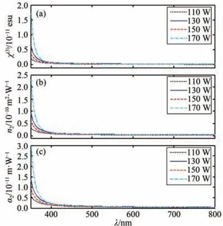
图9 不同功率时所制备薄膜的χ(3)-λ,n2-λ和α2-λ曲线Fig.9 The curves of χ(3)-λ,n2-λ and α2-λ for the thin films prepared at various powers
3 Conclusion
The TCO thin films of ZnO:Ga-Mg were prepared by magnetron sputtering.The effects of sputtering power on the microstructural,electrical and optical characteristics of the deposited films were investigated.The XRD analysis results show that all the deposited films have hexagonal wurtzite structure with highlycaxis preferred orientation along the(002)plane regardless of the sputtering powers.When the sputtering power is 150 W,the ZnO:Ga-Mg thin film possesses the best crystal quality and photoelectric properties,with the minimum resistivity,dislocation density and lattice strain,and the maximum figure of merit,average visible transmittance and mean particle size.The optical constants of all the deposited films were determined by the method of optical spectrum fitting from the measured transmittance data.It is observed that the refractive index and extinction coefficient tend to reduce with the increment of wavelength.Meanwhile,the dispersion behavior of the refractive index was analyzed by means of the single-oscillator WDD model,and the optical parameters including direct energygap,single-oscillator energy,dispersion energy,the first order of moment,the third order of moment,static refractive index and lattice dielectric constant were achieved.In addition,the dependence of nonlinear optical properties of the deposited films on sputtering power were also investigated in detail.The results demonstrate that the sputtering power is one of the most important deposition parameters to affect the microstructure,optical and electrical properties of ZnO:Ga-Mg TCO thin films.
