FPGA based hardware platform for trapped-ion-based multi-level quantum systems
2023-10-11MingDongZhu朱明东LinYan闫林XiQin秦熙WenZheZhang张闻哲YihengLin林毅恒andJiangfengDu杜江峰
Ming-Dong Zhu(朱明东), Lin Yan(闫林), Xi Qin(秦熙),Wen-Zhe Zhang(张闻哲), Yiheng Lin(林毅恒), and Jiangfeng Du(杜江峰),§
1CAS Key Laboratory of Microscale Magnetic Resonance and School of Physical Sciences,University of Science and Technology of China,Hefei 230026,China
2CAS Center for Excellence in Quantum Information and Quantum Physics,University of Science and Technology of China,Hefei 230026,China
3Hefei National Laboratory,University of Science and Technology of China,Hefei 230088,China
Keywords: FPGA,hardware platform,trapped-ion,multi-level quantum system
1.Introduction
The trapped-ion system[1–5]has been recognized as a potential platform for quantum simulation,[6–11]quantum computing,[12–15]quantum networking,[16]quantum sensing,[17,18]and quantum logic clock,[19–21]contributed by the favorable properties such as long coherence time,[24,25]near-perfect state preparation and readout,[24,25]and highfidelity quantum logic gate operations.[26,27]The trapped-ionbased two-level system have been used as a potential platform for quantum computation and quantum simulation,[1–15]whereas the multi-level quantum systems can provide a larger capacity to store process information.[28]The quantum controls for multi-level quantum system and high-dimensional quantum simulation are new research fields of the trappedions.[28–31]
In the experimental setup of the trapped-ion-based multilevel quantum systems, direct-current (DC) electrodes and global radio-frequency (RF) electrodes are used to generate the electrical field to trap the ions.[1,32]Multi-channel digitalto-analog-converter (DAC) based arbitrary waveform generators (AWGs)[33,34]and direct-digital-synthesis-based (DDS)RF generators[35]are used to generate the electrical signals for the electrodes.[36]The RF antenna, microwave (MW) antenna and the acousto-optic modulator(AOM)are used to deliver control signals from AWG channels or DDS RF channels to the ions for quantum state manipulation.[14]Pulse signals[35,37–40]are commonly applied to trigger the control signal generation channels, and to switch the control signals before delivered to the ions.[41]On the other hand, a high speed counter is employed to count the fluorescence photons output from the ion-based quantum systems,[42]and the proportion integration differentiation (PID) controller is utilized to lock the frequency of the laser transmitting through the AOM.[43]Commercial off-the-shelf(COTS)devices have been a practical solution to implement the hardware platforms for the trapped-ion-based quantum system,[44–48]whereas COTS are costly and lack of flexibility, and cannot meet the requirement of various experiments.Customized hardwares have been developed for the two-level ion systems,[49–52]and the specific requirements of the researchers can be achieved.An AWG board with a 50 Msps sampling rate is reported for fast ion transport and control operation pulse shaping,[49]whereas the hardware is not suitable to generate flexible waveforms at hundreds of MHz frequency which can be delivered to the antennas or AOMs.The researchers at Sandia National laboratories also report an AWG-based coherent control system with 2-tone signal generation and gate sequencer for multi-qubit MS gate realization.[50]A home-built hardware system M-Action[51,52]is developed with 4-channel DDSs,4-channel DACs and PID modules, to generate complex waveforms for two-level trapped-ion-based experimental platforms.However, the multi-level ion systems have more transitions compared to two-level systems.Hence, the AWG for multilevel systems needs to be designed to be capable of generating signals with multiple frequency signals, and more DDS channels are also required.The study on the implementation of the hardware platform for the multi-level ion systems will be meaningful to the further development of the trapped-ion quantum information.
This paper focuses on the technique of the control and readout hardware which is the interface between quantum systems and the classical systems.We present a hardware platform which can be applied in the study of the trappedion-based multi-level systems, and the platform is implemented with reconfigurable field-programmable-gate-arrays(FPGA)which can provide favorable flexibility for the experimental studies.A multiple channel AWG,[33,34]DDS modules,pulse generators,[37–40]PID controllers and a high speed counter[33,34]are implemented on the platform.The AWG channels can be configured to output mixed signals with four different frequencies.The synchronous control signals generation and the output signal readout of the multi-level ion system can be fully realized.Furthermore, the hardware platform is scalable and can also be applied in the future studies of scaled trapped-ion-based multi-level systems.
2.Architecture
The block diagram of the hardware platform for the trapped-ion-based multi-level systems and the connections between the hardware and the trapped9Be+ion system are shown in Fig.1.Four print-circuit-boards(PCB)are designed to implement the hardware.Communications between the host computer and the hardware are handled by a universal serial bus (USB) microcontroller CY68013A.In order to meet the requirements of the signal quality for long term experiments which last several days,a 10 MHz atomic clock FS725 with a 5×10-11monthly stability is integrated on the hardware, and the temporal stability of the output control signals can be ensured.Oscillators which have similar longterm stability can also be used to implement the hardware.Each board utilizes a Xilinx FPGA as the central control and data processing unit.The FPGA on the DDS board and the PID board is kintex XC7K160TFFG676,whereas AWG board uses virtex XC7VX485TFFG1761 and DAC board uses kintex XC7K410TFFG900.The clock buffer Si53340 which has a 50 fs root-mean-square (RMS) additive jitter is utilized to receive the 10 MHz system clock,and to output clock signals for each board.The phase-locked-loop (PLL) chip AD9518 is used to generate the high speed operating clocks for the DAC, the analog-to-digital-converter (ADC), and the DDS chips.The sixteen AD9910 DDS chips on the DDS board have a 1 giga samples per second (Gsps) sampling rate and a 14 bits amplitude resolution, whereas the performance parameter of the four AD9129 DAC chips on the AWG board is 2.8 Gsps@14 bits.The high amplitude resolution of the DDS board and the AWG board is helpful to realize quantum gates which has a fidelity exceeding 99.99%in the future studies.[53]Ten DAC AD9726 chips, which has a 100 Msps sampling rate and a 16 bits amplitude resolution, are located on the DAC board to provide DC and low frequency control signals for the static electrodes in the trapped-ion systems.[32,36]The DAC board has a±10 V output range, and the 16 bits DAC can contribute a minimum output resolution of better than 1 mV.Hence an ion position control precision of 10 nm within a 200 μm range can be achieved.[54]In order to realize the quantum state initialization, the DDS chips are configured to generate the 80–400 MHz RF frequency signals for the antennas and the AOM in the ion systems to output corresponding electromagnetic wave signals and laser signals.[14]The DDS channels are also used to output a 65 MHz signal for the outer RF electrode to control the position of the trapped ions.[55]The AWG channels are used to output RF signals with mixed frequencies which can be utilized to achieve quantum state manipulation for the ions.The PID board is fabricated with two 200 Msps@16 bits ADCs LTC2107 and a 200 Msps@16 bits DAC AD9783, and the laser frequency and power can be stabilized by applying the PID function.The DDS board is equipped with sixteen 8-ns resolution pulse output channels which have a 3.3 V low-voltage-transistortransistor-logic (LVTTL) voltage level, and the pulse signals can be used to modulate and switch the RF signals.The AWG board also has eight 8 ns resolution pulse channels to output trigger signals for additional boards when more signals generation channels are needed, in order to provide scalability for the platform.The 8 ns time resolution contributes to an infidelity of 0.00016% with a 10 μsπpulse width according to Ref.[53], hence the high fidelity quantum gate operation can be achieved.Two digital input channels are integrated on the DDS board,and the input digital signals are connected to the high speed counter inside the FPGA chip, hence the output photons from the experimental platform can be counted and recorded by the hardware.The variable gain amplifier(VGA) is used to amplify the output RF signals and the input signals with configurable gains.The DAC board,the DDS board and the AWG board operate simultaneously when applied to control the trapped-ion-based systems, whereas the PID board is used to control the power and the frequency of the laser systems.The FPGA chips are reconfigurable,hence the platform can be re-programmed without hardware modification to meet the requirement of various experiments, and favorable flexibility can be obtained.Table 1 shows the FPGA resource occupation of the hardware platform.Lookup-tables(LUTs),flip flops and slices are basic FPGA resources which can be programmed by the users.Digital-signal-processors(DSPs)are internally integrated digital processing modules inside the FPGA.Block-random-access-memories(BRAM)are integrated data storages inside the FPGA.Input and output(I/O)ports of the FPGA can also be configured by customers,and can provide signal transmission path for device control and signal generation.All the operating clock frequencies of the four boards are below 200 MHz,and the timing constrain design can be automatically performed by the Xilinx software Vivado.
The hardware has been applied in a three-level quantum system(qutrit)implemented with a trapped9Be+ion in a Paul trap.[1]In order to manipulate the qutrit, RF signals from the AWG board are connected to the antenna which can deliver the control signals for the qutrit.The DDS RF signals and the DC signals are connected to the electrodes which are used to trap the9Be+ion.The9Be+ion is cooled, initialed and readout by using 313 nm lasers.The power and frequency of the laser system are stabilized by the PID board.The laser pulse sequences are generated using acousto-optic modulators(AOMs)controlled by RF pulse sequences from the DDS board.A photo-multiplier tube (PMT) detector converts the fluorescence into digital pulses,and the pulses are counted by counters on the DDS board.The output digital signals from the DDS board are used to switch the AOM and trigger the AWG board.

Table 1.FPGA resource occupation of the reported boards.
The block diagrams of the pulse generator and the AWG inside the FPGA chip are shown in Fig.2.The pulse generator is designed with a time interpolating method according to Ref.[56],and an 8 ns coarse time resolution and a 52 ps fine delay adjustment resolution have been achieved.Figure 2(a)shows that the programmed FPGA logic of the pulse generator receives the digital pulse data from the host computer via the USB bus, and the data are pre-stored in the RAM memory inside the FPGA chip.The digital pulse data are cached by a first-in-first-out (FIFO) memory, and the 39 bits coarse data are received by a coarse counter which operates with a 125 MHz clock,and the 8 ns coarse time resolution pulse signals can be generated.The pulse signals can be further processed by the OSERDES module and the ODELAY module to achieve a fine time delay with a 52 ps resolution.Figure 2(b)shows the block diagram of the AWG,and the AWG can generate mixed sinusoidal signals with four different components.The amplitude,the frequency and the phase information of the AWG are also pre-store in the RAM inside the FPGA,cached by the FIFO, and then managed by each processing engine.The amplitude and the phase have a 12 bits resolution, and the frequency has a 40 bits resolution.The AWG FPGA logic operates with a 175 MHz clock whereas the sampling rate is 2.8 Gsps, hence 16 digital waveform calculation modules are implemented for each signal components.The Digital waveform data rate are accelerated by the OSERDES module to achieve a 2.8 Gsps@14 bits sampling performance,and finally be converted to analog signals by AD9129.All the boards of the hardware platform receive the operating clocks signals from the same atomic clock, and the DDS board can output pulse signals to trigger other boards.The delay time of the trigger signals can be adjusted with a 52 ps resolution, therefore the different boards can operate with coordinated timing by employing the fine resolution trigger signals.The duplication of the PCB boards can be parallel cascaded, and can be precisely synchronized using the picoseconds resolution trigger design.Hence, our hardware platform has a considerable scalability.

Fig.2.Block diagram of the pulse generator(a)and AWG(b)implemented with the FPGA logic.
3.Characteristics

Fig.3.Photograph of the hardware platform.The PCB board on the left is the 10-channel DAC board.The 16-channel DDS board is located at the center.The 4-channel AWG board and the PID board are on the right side.
The hardware platform has been designed and fabricated,and the photograph of the PCB boards is shown in Fig.3.The PCB board on the left is the 10-channel DAC board.The 16-channel DDS board is located at the center.The 4-channel AWG board and the PID board are on the right side.The hardware platform has been tested and characterized, and the test results are demonstrated as follows.
3.1.Spectrum performance
Lower noise DAC applied to electrodes for the ion-trap contributes to a lower heating rate which is a critical metric for quantum information processing.In order to demonstrate the noise performance of the DAC,we measure the 0 V,+10 V,and-10 V output spectrums with a Keysight N9030B spectrum analyzer.The test result is shown in Fig.4(a), and the averaged DAC noise density within 20 Hz to 1 MHz for 0 V,+10 V, and-10 V outputs are 69.9 nV/Hz, 130 nV/Hz and 131 nV/Hz, respectively.The low DAC noise ensures the ion position control precision.The phase noise of the DDS board and the AWG board is an important metric since low phase noise contributes to high fidelity,[53]and the phase noise is also recorded by the spectrum analyzer.Figure 4(b)shows the phase noise curves of the 10 MHz reference clock from FS725, as well as the phase noise of the 10 MHz and the 100 MHz carriers from the DDS board.At 100 kHz frequency offset,the measured phase noise of the 10 MHz clock is-129.0 dBc/Hz, and the phase noise of the 10 MHz carriers from the single DDS channel is-128.6 dBc/Hz,whereas the phase noise of the 100 MHz carriers is-124.2 dBc/Hz.The phase noise of the AWG board is also measured and the result is shown in Fig.4(c).The phase noise of the 10 MHz and the 100 MHz carriers of single AWG channel at 100 kHz frequency offset are-128.6 dBc/Hz and-126.8 dBc/Hz,respectively.Due to the difference of the architecture inside the analog chip, the phase noise of the DDS board is worse than that of the AWG.The DDS chips are applied for cost reasons as their price is much lower than that of the high speed DAC on the AWG board.

Fig.4.Spectrum results of the hardware platform.(a)Power spectrum of the DAC board when output 0 V,+10 V,and-10 V signals.(b)Phase noise of the DDS board.(c)Phase noise of the AWG board.
3.2.Pulse signals
The output signals of the pulse channels are recorded by a LeCroy WaveMaster 820Zi-B oscilloscope which has an 80 Gsps sampling rate and a 20 GHz bandwidth, and the oscillograms are shown in Fig.5(a).The pulse channels can output pulse signals with programmable pulse width which has a nanosecond resolution.The time jitter which is determined by the phase noise of the clock source as well as the circuit noise,stands for the stability of the digital pulse signals.The jitter performance of the pulse outputs is also measured using the oscilloscope.The time histograms of measuring time intervals between two pulse channels are shown in Figs.5(b)(pulse channels from the same DDS board) and 5(c) (pulse channels from DDS board and AWG board respectively).Figure 5(b) shows that the jitter of the digital output is 8.6 ps which leads to a low infidelity of 1.82×10⁻¹², and the time jitter in Fig.5(c) is 24.4 ps corresponding to a infidelity of 5.16×10⁻¹².The reason why it has a negative mean value is that the arrival time of the pulse signals from the second channel is earlier than that from the first channel,and a subtraction is performed to calculate the time interval.The long tail of the histogram is caused by the circuit noise and the clock noise,and the maximum deviation is below 100 ps.Hence the performance of the pulse channels can meet the requirements of the trapped-ion based quantum experiments.

Fig.5.Characteristics of the digital output channels.(a)Oscillogram of the pulse signals from pulse channels.(b)Histogram for measuring time intervals from pulse channels on the same board.(c)Histogram for measuring time intervals from the pulse channels on the DDS board and the AWG board.
3.3.PID feedback test
The PID board is employed to achieve the stabilization for laser power and frequency.The long-term performance of the power stabilization is demonstrated by a 100 seconds acquisition of unlock-to-locked test.As shown in Fig.6(a),the standard deviations of unlocked and locked photodiode(PD) output are 4.96 mVRMSand 0.77 mVRMS, respectively.Therefore, the infidelity of the quantum gate can be reduced from 0.066%to 0.0016%by using the PID to control the laser power.[53]The PID board is also applied to lock the frequency of laser.In order to verify the long-term behavior, the frequency error of the laser is acquired through a 200 seconds test, with frequency unlock for 100 seconds and locked for another 100 seconds,and the result is shown in Fig.6(c).The standard deviations of unlocked and locked laser frequency are 5.86 MHzRMSand 0.46 MHzRMS,respectively.Hence,the infidelity for quantum state detection can be reduced from 3.1%to 0.0030%accordingly.[57,58]Figures 6(b)and 6(d)show the long-term Allan deviation measurement with a 2000 s integration time.After the PID is turned on for 0.01 s, the Allan deviations of the laser power and frequency are below 10-4and 10-10,respectively.
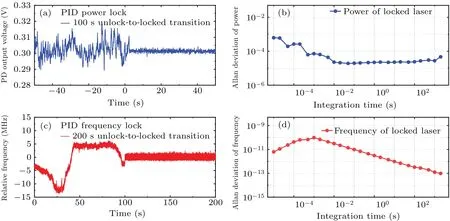
Fig.6.Test results of applying the PID board to control the power(a),(b)and the frequency(c),(d)of the laser systems.The power and the frequency of the laser systems become more stable after the PID board is applied.(b)and(d)The Allan deviation measurement with a 2000 s integration time.
4.Experimental test results
In order to demonstrate the performance of the hardware platform when applied in the trapped-ion-based multi-level quantum system,we applied the hardware platform to perform the three-level experiments, and the PCB boards are located on a retainer plate of the experimental platform.A9Be+ion with an ambient magnetic field at 119 Gauss from a pair of Sm2Co17permanent magnets and magnetic field compensation coils,[59]is used to realize the experiments.The ground state energy levels can be labels as|F,mF〉whereF={1,2}is the total spin angular momentum,mF={-F,-F+1,...,F}is the projection of total spin angular momentum along the quantization axis aligned with the magnetic field.[58]Three levels|F= 2,mF= 2〉,|2,1〉 and|1,1〉 are employed to represent the three-level quantum system (qutrit), labeled as{|0〉,|1〉,|2〉}, with corresponding transition frequencies.At the beginning of experiments, the ion is Doppler cooled[1]using a series of laser pulses, followed by state initialization with optical pumping.[1]To determine the resonant frequencies, the frequencies applied to microwave (MW) and radio-frequency (RF) antennas are scanned and the fluorescence photons are counted, as detailed in Section 5.The result is shown in Fig.7(a) and the resonant frequencies are 102.616(1) MHz, 1018.052(2) MHz, 1120.9127(6) MHz, respectively.By scanning the pulse duration at resonant frequency with full power, the Rabi oscillations are acquired in Fig.7(b) which indicates the resonantπ-pulse durations of transitions|0〉↔|1〉,|0〉↔|2〉,|1〉↔|2〉 are 12.01(10) μs,16.20(14)μs,20.31(20)μs,respectively.
As the coherence time is critical to characterize the performance of the quantum information processing,[41]the applied operation is Ramsey experiment in which the qutrit firstly is prepared in (|0〉+|1〉+|2〉)/3,[60]evolving with varied Ramsey intervals without protection and mapped to|0〉 state by applying readout pulses.As shown in Fig.7(c),1.46(9) ms coherence time is acquired with a Gaussian decay.After applying four repetitions of the multilevel dynamical decoupling (MLDD)[60,61]sequence, the coherence time is extended to 18.7(23)ms according to the result in Fig.7(d).To characterize the operation fidelity,randomized benchmarking method[62]is applied, and according to the results shown in Fig.7(e), the average gate fidelities of the three transitions|0〉↔|1〉,|0〉↔|2〉,|1〉↔|2〉 are 99.95(2)%, 99.8(1)% and 99.5(3)%, respectively.As the fidelity becomes worse than 0.8, the dots on the red line and the blue line stop when the number of gates is greater than 100.The operation fidelities are sufficient for most quantum simulations,[63]and the fidelity can be at least 90% for 20 gates.The infidelity contributed by noise from the hardware is much lower than that from the experimental platform itself, and the infidelity contribution from the hardware circuits can be ignored.Hence,the hardware platform is suitable to be applied to perform high fidelity trapped-ion-based multi-level quantum experiments.

Fig.7.Characteristics of the three-level quantum system(qutrit)consisted of|F =2, mF =2〉, |2,1〉and|1,1〉of the ground states of 9Be+.(a)Ion fluorescence collected by PMT while scanning the frequency, the dip indicates the resonant frequency.(b) Rabi oscillations of qutrit transitions.(c)Ramsey experiment without protection for coherence time measurement.(d)Ramsey experiment with MLDD-4 protection for coherence timemeasurement.(e)The randomized benchmarking result of the 3 transitions.
5.Discussion
5.1.DAC output signals
The DACs generate DC or sequence signals to control the spatial position of ions.The static DC voltages are applied for ion loading and can be finely tuned for micro-motion compensation.The DACs can also operate at 100 Msps sample rate to generate sequence signals with a 10 ns temporal resolution which is much lower than the ions’motional period(typically 300 ns–1000 ns).Hence, the ion’s fast transport can be realized at a time scale of dozens of microseconds, whereas the adiabatic transport costs hundreds of microseconds.[49]
5.2.Numbers of DDS channels and AWG channels
The DDS channels and the AWG channels are applied to generate control signals which are delivered to the RF electrode potential,the antennas and the AOM drivers in the laser system.In order to realize the ion confinement and optical initialization for the three-level9Be+trapped-ion platform, one DDS channel is assigned to the RF electrode potential,and ten DDS channels are required to control the AOM drivers for the lasers.On the other hand, three AWG channels are applied to one RF antenna and one MW antenna to realize three-level quantum logic gate in form of RF/MW transitions.Similar channel assignment can be applied for other ion species,such as40Ca+,171Yb+, etc.The required numbers of DDS channels and AWG channels will increase once mixed-species ions or scaled multi-level ions are applied.
5.3.Digital input channels
The digital input channels which are integrated on the DDS board are implemented with FPGA-based triggered counters which has an 8 ns time resolution, hence the electrical pulses output from the experimental platform can be recorded.Digital input channels can also be used as external trigger ports.The trigger-to-output latencies for the AWG board,the DDS board,and the DAC board are measured to be 50 ns,100 ns,and 650 ns,respectively.The latencies are much lower than the coherence time of the ions,hence the hardware platform also has the potential to be further applied to realize the close-loop feedback control for the ions.The FPGA chip on the DDS board can be programmed to manage the feedback operations, and the feedback information can be shared with other boards via the digital output channels.
5.4.Comparison with other studies
The comparison between this work and the hardware designs for tapped-ion based two-level systems is shown in Table 2.A 50 Msps sampling rate AWG is reported for fast ion transport through applying the voltages to trap electrodes.[49]In order to realize the multi-qubit coherent control, an 8-channel 819.2 Msps AWG with a 14 bits vertical resolution is implemented with a Xilinx rf system-on-chip(RFSoC).[50]A home-built hardware system for mixed-species ion qubits is reported in Ref.[52], and DDS boards, DAC boards and PID boards are implemented.As the coherent control is based on DDS chips which is suitable for single frequency generation whereas such solution lacks flexibility, the AWG modules are required to generate user-defined waveform for multilevel trapped-ion based quantum systems.On the other hand,the COTS ARTIQ platform[44–48]can achieve similar performance, whereas our design has a stronger power in multifrequency signal generation which is meaningful to the study of ion qudit.The hardware platform QICK[64]which is designed for superconducting quantum systems has overlaps with the hardware for ion-based system, whereas the DDS channels and the PID designs are not included.In this paper,the reported hardware platform which is composed of the DDS board, the AWG board, the DAC board and the PID board can provide more signal generation channels compared to the hardware for the two-level ion systems.The platform is reconfigurable, and the control for the multi-level trapped ion quantum system can be fully managed.

Table 2.Performance comparison with related hardware.
6.Conclusion
We report the design and implementation of a high performance hardware platform for the trapped-ion-based multilevel systems.A 10-channel DAC board, a 16-channel DDS board,a 4-channel AWG board and a PID board are fabricated to realize the platform.The characteristics of the hardware platform have been tested,and the performance has been confirmed by the experimental results on a three-level quantum system using a trapped9Be+ion.The hardware platform is scalable and is also promising for the applications of scaled trapped-ion-based multi-level systems.
Acknowledgements
Project supported by the Strategic Priority Research Program of CAS (Grant No.XDC07020200), the National Key R&D Program of China (Grants No.2018YFA0306600),the National Natural Science Foundation of China (Grant Nos.11974330 and 92165206), the Chinese Academy of Sciences (Grant No.QYZDY-SSW-SLH004), the Innovation Program for Quantum Science and Technology (Grant Nos.2021ZD0302200 and 2021ZD0301603), the Anhui Initiative in Quantum Information Technologies (Grant No.AHY050000),the Hefei Comprehensive National Science Center, and the Fundamental Research Funds for the Central Universities.
杂志排行

Chinese Physics B的其它文章
- Dynamic responses of an energy harvesting system based on piezoelectric and electromagnetic mechanisms under colored noise
- Intervention against information diffusion in static and temporal coupling networks
- Turing pattern selection for a plant–wrack model with cross-diffusion
- Quantum correlation enhanced bound of the information exclusion principle
- Floquet dynamical quantum phase transitions in transverse XY spin chains under periodic kickings
- Generalized uncertainty principle from long-range kernel effects:The case of the Hawking black hole temperature