High performance solar-blind deep ultraviolet photodetectors via β-phase(In0.09Ga0.91)2O3 single crystalline film
2023-10-11BichengWang王必成ZiyingTang汤梓荧HuyingZheng郑湖颖LishengWang王立胜YaqiWang王亚琪RunchenWang王润晨ZhirenQiu丘志仁andHaiZhu朱海
Bicheng Wang(王必成), Ziying Tang(汤梓荧), Huying Zheng(郑湖颖), Lisheng Wang(王立胜),Yaqi Wang(王亚琪), Runchen Wang(王润晨), Zhiren Qiu(丘志仁),†, and Hai Zhu(朱海),2,‡
1State Key Laboratory of Optoelectronic Materials and Technologies,School of Physics,Sun Yat-Sen University,Guangzhou 510275,China
2Guangdong Provincial Key Laboratory of Magnetoelectric Physics and Devices,School of Physics,Sun Yat-sen University,Guangzhou 510275,China
Keywords: deep ultraviolet,film,photodetector,heteroepitaxy
1.Introduction
Solar irradiation with wavelength shorter than 280 nm,commonly known as the solar-blind range,is rarely present at the Earth’s surface due to the strong absorption of deep ultraviolet(DUV)light by the ozone layer,water vapor and fine particles in the atmosphere.[1]As a result,photodetectors operating in this spectral range, as solar-blind photodetectors, have the advantages of low bit error rates and high signal-to-noise ratios.[2]These photodetectors have a wide range of important applications in industry,environmental protection,monitoring of the ozone layer, and the military.[1,3–6]Therefore, solarblind photodetectors have received extensive attention and high research enthusiasm.Narrow-bandgap semiconductors,such as silicon semiconductors, have been largely limited in the development of solar-blind photodetectors due to the low ultraviolet light sensitivity and poor thermal stability.[7]The ultra-wide bandgap semiconductors have large bandgaps and high Baliga figures of merit (BFOMs), providing incomparable advantages in terms of breakdown resistance,low leakage,and low loss.[8–10]In recent years, ultra-wide bandgap semiconductor materials,including aluminum nitride(AlN),[11–13]diamond,[5,14,15]β-phase gallium oxide (β-Ga2O3),[2,16–24]aluminum gallium nitride (AlGaN),[25,26]aluminum gallium oxide (AlGaO),[27]magnesium zinc oxide (MaZnO)[28]and InGaO[29–32]have been used to fabricate solar-blind photodetectors.As an important member of ultrawide bandgap semiconductors, the bandgap (BFOM) ofβ-Ga2O3is 4.9 eV(3000).Furthermore,β-Ga2O3exhibits a significant absorption in the solar-blind range, exceptional thermal and chemical stability.Therefore,Ga2O3-based semiconductor is an excellent material for the preparation of solar-blind DUV photodetectors,which has high responsivity and external quantum efficiency.[24,33,34]Although manyβ-Ga2O3solar-blind detectors have been reported to have excellent performance,they are limited by the fact thatβ-Ga2O3only has a single bandgap.
In order to realize the manipulation ofβ-Ga2O3bandgap flexiblility,the Ga2O3host crystal lattice can be doped with Al or In atom.Due to the similar diameter between the In and Ga atoms,the In is an ideal candidate for dopingβ-Ga2O3.[35,36]The bandgap of InGaO alloy system can be manipulated by adjusting the atom components ratio.[31,37]This doping scheme will allow the fabricated detector to cover a wider spectral range and enhance parameters such as responsibility.[29,31]
Swallowet al.utilized density functional theory(DFT)to determine the electronic structure of InGaO alloys and discovered that the density of the In 4d state in In2O3is higher than that of the Ga 3d state in Ga2O3,indicating that InGaO has an increased density of states in the valence band due to the presence of indium.[38]This increase In density results in stronger light absorption,especially in the deep ultraviolet range.Consequently, the InGaO solar-blind detector produces a higher density of photoexcited carriers than that of the Ga2O3solarblind detector under deep ultraviolet light irradiation.Additionally, indium doping introduces In 5s orbital at the bottom of the conduction band,which enhances the transport of photogenerated carrier.Because In 5s orbital has a larger spatial expansion than that of Ga 4s orbital, the electron mobility is higher.[39]In conclusion,the In-modulated electronic structure in Ga2O3significantly improves the performance of the InGaO solar-blind photodetector.
In this article, the realization of high-performance In-GaO alloy based solar-blind photodetector is reported at room-temperature (RT).The InGaO film is grown oncplane sapphire by plasma-assisted molecular beam epitaxy.Typical schottky junction is constructed between interdigital electrodes and InGaO film with metal–semicondutor–metal(MSM) configuration.The dark current of device is as low as 40 pA,while it’s responsivity is as high as 450 A/W(50 V).The UV/VIS rejection ratio of device (R232nm/R380nm) exceeds 4×10⁴, which demonstrates the excellent solar-blind selectivity response character.The transient response test gives the rising and falling time of the device are only 80 ns and 420 ns, respectively.Moreover, an unambiguous twodimensional scanning imaging pattern provided by InGaO solar-blind detectors is also demonstrated.
2.Experimental procedures
InGaO film was grown on 2 inches sapphire (0001) by PA-MBE(SVT 35-V-3).The sapphire substrate was annealed at 750°C for 15 min at an oxygen flow rate of 1.6 sccm.Firstly, high-purity (6N) gallium source was evaporated onto the substrate.Then,a low temperature(200°C)Ga2O3buffer layer was grown.Afterwards, a high temperature Ga2O3buffer later was grown for 1 h at temperature of 950°C for the Ga source and 700°C for the substrate while maintaining the oxygen flow rate.To introduce the indium source,the indium source temperature was raised to 550°C and the indium gallium oxide grown for 1 h.After InGaO growth,the surface topography and thickness of the film were characterized by field-emission scanning electron microscopy (SEM, Hitachi S-4800), and the surface roughness of the film was measured using the tapping mode of the atomic force microscopy(AFM,Veeco Dimension Edge).X-ray diffraction instruments(XRD,Bruker Discover&Advance)were used to determine the crystal structure and growth quality of the thin film.The spectrometer (Shimadzu UV-2700) can test the transmittance and absorption optical properties of the sample.Then x-ray photoelectron spectroscopy(XPS,Escalab 250 Xi, Thermo Fisher)was tested on the InGaO film to obtain the composition content information of the film.The solar-blind photodetector devices were designed to be 50 pairs of interdigital electrodes(Ti/Au 20 nm/50 nm) with interfingers spacing of 6 μm that evaporated by electron beam(EB,Oxford Cryo-Plex 8)on In-GaO film.For electrical measurements of the detector,theI–Vcharacteristics and responsivity of device were carried out with a multifunctional digital source measure unit (Keysight B2902A) when a 150 W Xe lamp was used as an ultraviolet light excitation source.The transient photoresponse test of detector was recorded by an oscilloscope (Teledyne LeCroy HDO4304) under 193 nm pulse laser (GAM laser EX5 EXCIMER laser).
3.Results and discussion
In this paper, high-quality InGaO thin films are grown on sapphire (001) using the plasma-assisted molecular beam epitaxy (PA-MBE).First, the sapphire substrate is annealed at 750°C for 15 min before growth to remove impurities on the substrate surface.Then, in order to release the mismatch between sapphire and InGaO, Ga/Ga2O3buffer layers are first grown on the sapphire substrate.Here,the Ga atomic layer can release interfacial strain due to its inherent ductility.Meanwhile, the low-temperature Ga2O3buffer layer acts as a nucleation site,and the high-temperature buffer layer provides a smooth plane for growth.After the deposition of the buffer layer, a uniform thin film of InGaO is grown at high substrate temperature for 1 h.A schematic diagram of the growth process of InGaO is shown (Fig.1(a)).During the growth process, the flux of oxygen atoms is greater than that of Ga atoms,which is due to the fact that oxygen-rich conditions can inhibit the formation of suboxide Ga2O and reduce the decomposition rate of GaOxon the substrate surface.[40,41]To monitor InGaO crystal quality during the growth process,reflection high energy electron diffraction (RHEED) patterns are recorded(Fig.1(b)).It can be seen that the diffraction patterns of the InGaO thin film are sharp linear shape,indicating that the surface during the growth process is very flat and the atoms on the surface are arranged in an orderly manner,which confirms that the epitaxial InGaO layer is a high-quality single crystal film with a two-dimensional planar growth mode.
The field-emission SEM surface topography of as-grown InGaO alloy film via MBE is depicted in Fig.1(d), meanwhile, the cross-sectional image of sample is given (inset of Fig.1(d)).It is noted that the thin film of InGaO presents compact and dense crystallization with a thickness of around 300 nm.The smooth surface of the film without pits can be seen obviously, which indicates that the fabricated InGaO alloy film is a high crystalline quality film.Figure 1(e) displays the AFM surface image of the InGaO thin film, it can be obtained that the as-grown InGaO film is extremely smooth with a root mean square (RMS) of 0.54 nm in the region of 5 μm×5 μm.

Fig.1.Growth and surface morphology of InGaO.(a) Growth diagram of InGaO thin film on sapphire substrate.The two designed buffer layers are deposited sequentially to reduce mismatches between the epitaxial film and the substrate.(b) and (c) RHEED patterns of InGaO thin film growth along [010] azimuth for 10 min and 30 min.(d) SEM image of InGaO thin film surface.The cross-section displays that the thin film exhibits dense crystallization, with a thickness of 300 nm(insert).(e) The atom AFM scanning image of InGaO hetero-epitaxy film.Here,the RMS of film is about 0.54 nm.
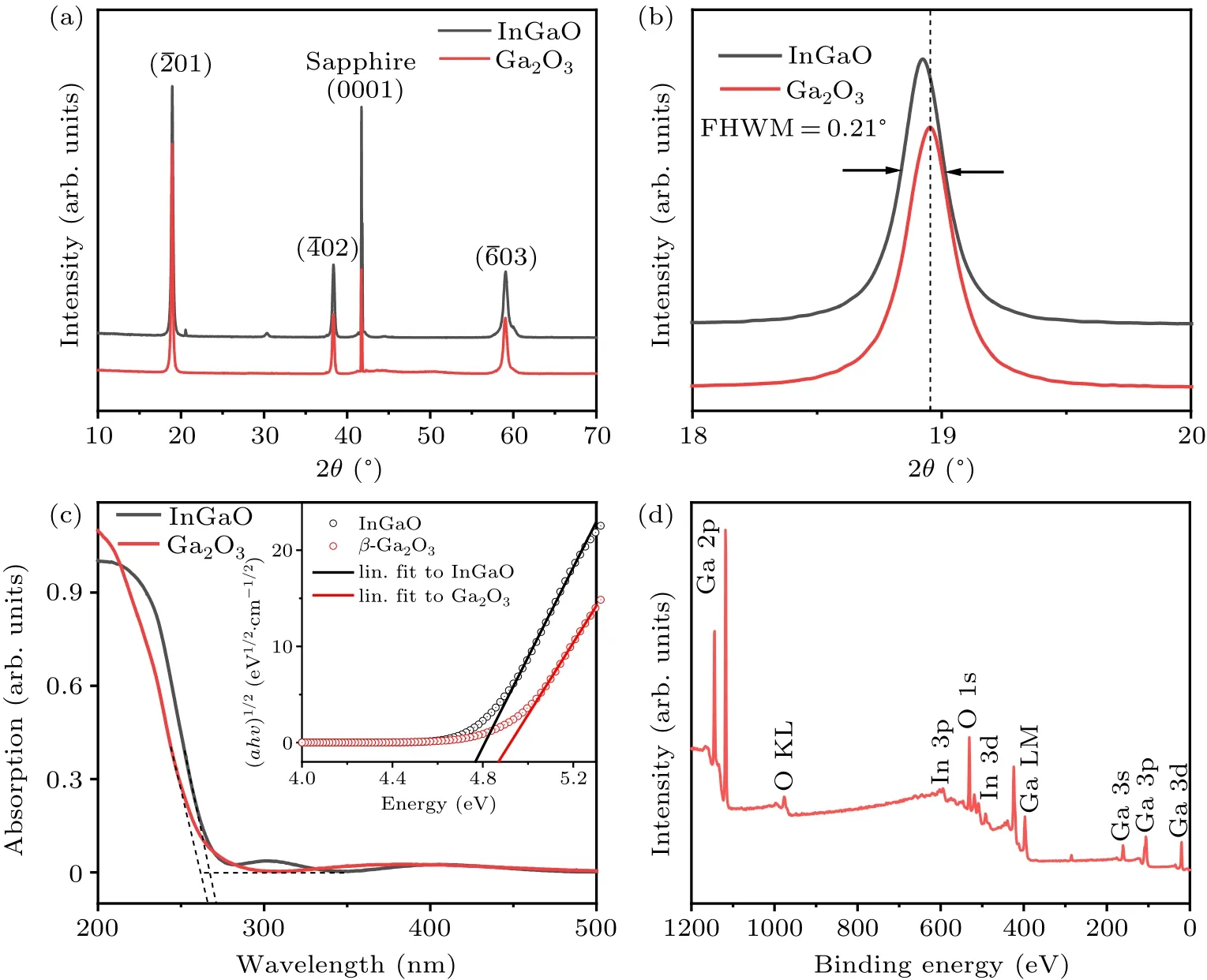
Figure 2(a) presents the XRD patterns of InGaO sample and pureβ-Ga2O3thin film.In addition to the characteristic peak of sapphire (0006) at 41.81°, both InGaO andβ-Ga2O3films contain three typical diffraction peaks at around 18.92°, 38.36°, and 59.08°, which correspond to its three crystal planes (¯201), (¯402), and (¯603), respectively.[21]Figure 2(b) shows the XRD pattern around the (¯201) diffraction peak which can be seen that the (¯201) diffraction peak of In-GaO has an obvious blue shift, and the FHWM is 0.21°, indicating that high-quality single-crystal thin films have been achieved.Furthermore, the InGaO sample has a blue shift of about 0.03°relative to Ga2O3,which is due to the larger diameter of the indium atom than that of the gallium atom,resulting in a larger lattice constant.[29]It can be seen from XRD pattern that the quality of InGaO film is very excellent.
Then, the ultraviolet-visible optical absorption spectrum test between the InGaO and Ga2O3thin films is carried out to compare the difference in optical properties.As shown in Fig.2(c),both InGaO and Ga2O3thin films have obvious absorption in the sola-blind band, and the absorption peak cutoff wavelength of InGaO(Ga2O3)is 266(257)nm.The inset of Fig.2(c) displays the relationship between (αhν) andEg,which is calculated according to the Tauc formula combined bandgap of the film[32]
wherehνis the incident photon energy,Egis the band-gap,andAis a constant.[30]Based on Eq.(1), the bandgap of the InGaO film is 4.76 eV, which is smaller than the bandgap of Ga2O3(4.87 eV).It can be concluded that the doping of indium can effectively regulate the bandgap of Ga2O3.
To determine the indium content of the film, XPS spectrum is presented in Fig.2(d), which shows the presence of all elements,and their concentrations are calculated using the integrated peak area ratio given by
whereAiis the integral area of elementi, andnis the total number of elements contained.The indium,gallium,and oxygen concentrations are found to be 2.7%, 28.4%, and 68.8%,respectively.Accordingly, the value ofXlnis estimated to be approximately 0.09 in InGO, which is consistent with the bandgap value obtained from the Tauc plot in Fig.2(c).Hence,the flexible doping technique for the InGaO alloy films using PA-MBE is feasible,which serves as a foundation for the fabrication of high performance solar-blind detectors.
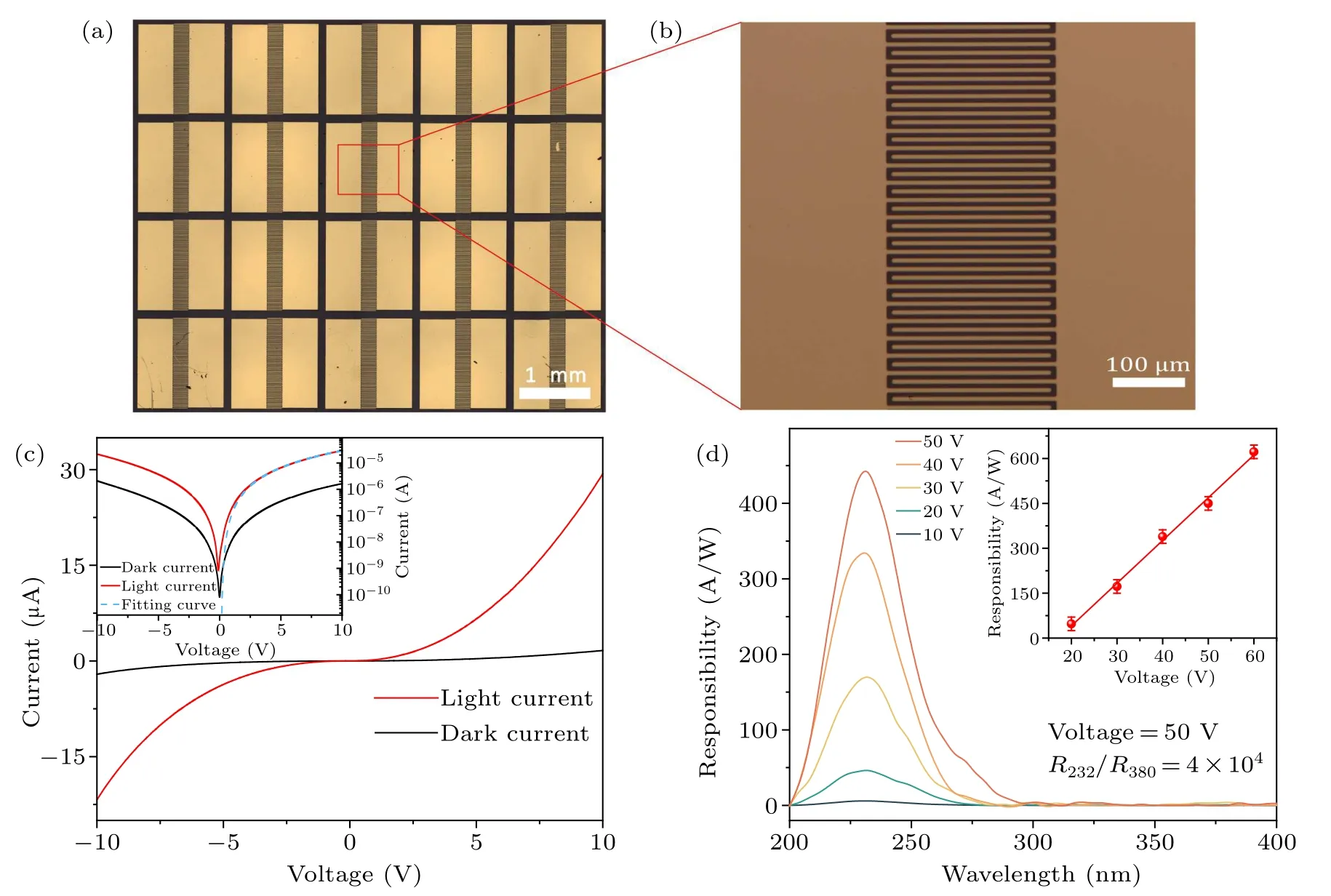
Based on the high-quality InGaO film, the MSM-type solar-blind photodetectors with interdigital electrodes configuration are constructed.Figure 3(a) illustrates the 4×5 matrix of the fabricated solar-blind detectors,where each device’s surface appears clean without any impurities.On the other hand,Fig.3(b)shows the physical image of the InGaO solarblind DUV photodetector.As can be seen,the width and spacing of fingers are both equal to 6 μm,and the total number of interdigitated electrodes is 50 pairs.
Figure 3(c) displays theI–Vcharacteristic of the photodetector under 232 nm light illumination and dark condition, respectively.The inset presents theI–Vcurve in semilogarithmic coordinates to distinguish the dark currents.Without DUV irradiation, the dark current of device is as low as 40 pA at zero bias.With increase of the bias voltage, the photon/dark current plots exhibit an obvious rectification characteristic.Above nonlinearly photon/darkI–Vproperties of device originate from the Schottky barrier between the Ti/Au and InGaO films.The current of the device is mainly tunneling current through metal/semiconductor interface for InGaO Schottky junction.At high external bias, the field emission(FE)current will dominate and can be described as[42]
Based on Eq.(3), the fitting of theI–Vcurves shows that the field emission component dominates the carrier transport at high voltage (inset of Fig.3(d)).The fitted curve closely matches the experimental data.

Fig.2.The crystalline properties of InGaO alloy film grown on sapphire substrate.(a)The XRD patterns of InGaO alloy and β-Ga2O3.(b)The XRD pattern around the(¯201)diffraction peak.It can be seen that the(201)diffraction peak of InGaO has an obvious blue shift,and the FHWM is 0.21°.(c)The absorption spectrum of InGaO alloy film and β-Ga2O3 at room-temperature,its cut-off peak is 267 nm.Insert: the relationship between(αhν)and Eg.The optical bandgap of sample is estimated via Tauc plot.(d)XPS spectrum of InGaO alloy films grown on sapphire substrates.Composition estimated from XPS measurements is calculated using peak areas rather than exact peak positions.XPS measurement results show that XIn=0.09 in InGO.

Fig.3.The InGaO alloy ultraviolet photodetector and photon response.(a) 4×5 solar-blind photodetector matrix.(b) Enlargerd SBPDs devices are constructed with interdigital Ti/Au electrodes(20 nm/50 nm)with interfingers spacing of 6 μm that are fabricated via photolithography.(c)The characteristic I–V curve of InGaO detector corresponds to DUV light and dark current of the device respectively.Insert: the I–V plots that are described in semi-log coordinates.(d) The typical photon responsibility spectra of the InGaO detector at RT.Insert: the responsibility of device as a function of the externally applied voltage.
When the bias voltage reaches 10 V,the DUV photoncurrent of the device is as high as 30 μA.The photo-to-dark ratio(PDCR) can give the detail information about the signal-tonoise ratio of detector,which is described as follows:[16]
whereIPis the photoncurrent under irradiation of 232 nm andIdis the dark current.The value of PDCR can be obtained as high as 20 at 10 V, indicating that the as-grown InGaO photodetector exhibits an excellent signal-to-noise ratio.
As one of the critical parameters of a detector,photon responsivity refers to the magnitude of photocurrent under the illumination of a unit of light power.The responsivity can be calculated as[43]
wherePis light power.As shown in Fig.3(d),the photon responsivity peak corresponds to a wavelength of 232 nm.Under the applied bias voltage of 50 V,the value of responsivity peak can increase to be as high as 450 A/W.Meanwhile the magnitude of UV/VIS suppression ratio(R232nm/R380nm)can be extracted to be about 4×10⁴from the plot.It should be noted that almost no obvious response of the detector in visible light region is observed, which demonstrates a cracking solar-blind selection characteristic.
The inset of Fig.3(d) displays the relationship between responsivity and applied bias voltage.It can be observed that the responsivity increases linearly with the increase in bias voltage.Furthermore, the device does not exhibit any saturation or breakdown phenomenon even when the bias voltage reaches 60 V,demonstrating that the device can stably operate under high voltage at room temperature.
The external quantum efficiency(EQE)of the device can be calculated from the optical responsivity using[20]
wherehis the Planck constant,cis the speed of light,λis the corresponding wavelength,andRλis the responsivity corresponding to the wavelength.Under an external bias voltage of 50 V, the calculation shows that, EQE=2×10⁵%, which proves that the device has great muscle augmentation.
The noise equivalent power (NEP) represents the minimum incident optical power required for the signal-to-noise ratio (SNR) to reach 1, and is calculated using the following equation:[32]
To further measure the performance of the solar blind detector,special detectivity can be calculated by[32]
whereAis the effective area of the device with a value of 0.18 mm2, and Δfrepresents the bandwidth, which is equal to 1 Hz.Therefore,special detectivity of the solar-blind detector is 2×10⁸Jones, demonstrating the superior performance of the device.

Fig.4.The temporal dynamic characteristics of InGaO alloy film solarblind photodetectors.(a)The transient photo-response of device with the irradiation of nanosecond pulsed laser.Here,the red solid line is a fitting curve according to a double exponential formula.Detector exhibits an extremely fast response speed and short restoring time.(b)Response time plots for different voltages.As the applied voltage increases,the lifetime of the device is slowly decreasing,and there is a tendency to saturation.
In order to investigate the temporal dynamic properties of our InGaO solar-blind detector,we perform measurements of the instantaneous response kinetics of the device.The response time of photodetector is defined as the time it takes for the photon current to rise(or fall)to 1/e of its maximum value when the irradiation light is turned on or off.Figure 4 depicts the instantaneous response curve of the InGaO detector under pulsed 193 nm laser excitation.Experimental data can be fitted with double exponential function
whereI0represents steady-state current,τ1andτ2are the response times, andA1andA2are the coefficients associated with the response times.As can be seen from Fig.4(a), the device exhibits an extremely fast response speed under pulsed laser irradiation.The rising time of the device,extracted from the rising edge of the plot, is approximately 80 ns.Transient drop timeτ1=420 ns andτ2=6.3 μs are deduced from the good agreement fitting curve.By varying the voltage, different response times are obtained (Fig.4(b)).As the applied voltage increasing, the response time of the device gradually decreases, which is due to the gradual increase of the carrier drift speed under the action of a strong electric field.However,when the load voltage is further increased,the probability of carrier-lattice collision increases so that the drift velocity reaches an extreme value.Therefore,the response time of the device is also saturated.

Table 1.Comparison of several reported solar-blind detectors with important parameters.

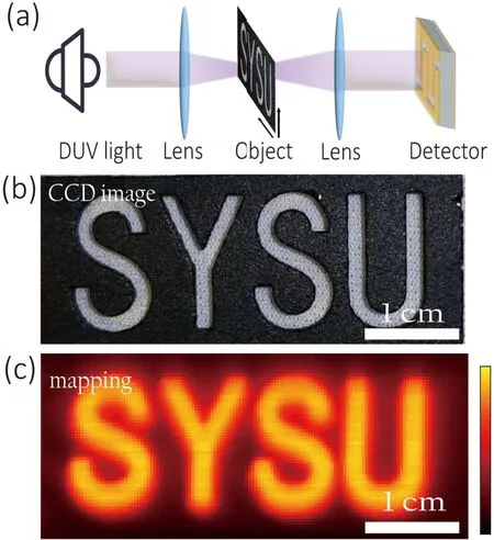
Fig.5.The imaging properties of InGaO detector.(a)Schematic diagram of imaging test system.Here, a InGaO film DUV photodetector plays a role as an imaging unit under external voltage.(b) The photograph of the two-dimensional(2D)object with several words SYSU.(c)The mapping image of the photon current corresponds to the profile of object.The scanning image exhibits a sharp edge, which is very similar to hollow letters.
In addition,the decay time obtained by the experiment is much shorter than that of most reported Ga2O3-based devices.τ1andτ2correspond to two different relaxation mechanisms.Among them,τ1is mainly due to the formation of recombination center energy levels in the interior and surface of the film.Rapid carriers transport between the interdigitated Ti/Au electrode and the thin film under an applied electric field.When the 193 nm laser is turned off,the current-carrying concentration drops rapidly,andτ1can be further optimized by changing the interdigital electrode parameters, annealing, etc.The parameterτ2is primarily associated with persistent photoconductivity(PPC).In InGaO film,traps capture minority carriers,and these carriers that fall into the traps cannot recombine directly.Instead,they recombine through recombination centers,resulting in slow decay characteristics of photonresponse.[7]In addition,τ2is also related to factors such as laser power and device parasitic capacitance.The ratio ofA1/A2is 16,which proves that the transport of photogenerated carriers between the electrode accounts for the main part of the device.Both the fast rise and fall exhibited by our device indicate its excellent fast response capability.
Table 1 summarizes various solar-blind detectors related to gallium oxide and their important parameters.Our devices exhibit remarkably high responsivity and fast response speed.
Additionally, the DUV scanning imaging capability is critical faculty for solar-blind photodetector.A self-designed scanning detecting system as shown in Fig.5(a)is constructed to evaluate the imaging performance of the device.Among them, Xe lamp provides DUV light and places the imaging object at the focal point of the first lens.DUV light passes through the second lens and parallel exits to the detector.Under ultraviolet light,the object with the word SYSU(Fig.5(b)) moves through the two-dimensional mobile platform.A source meter is used to provide an external bias voltage of 20 V and the computer records the current conditions at different positions.Finally, the current intensity at different locations is imaged.It can be observed from Fig.5(c)that the imaging of the current intensity is very similar to the object and has obvious boundaries.The wonderful performance demonstrates that the system has excellent fidelity characteristics and InGaO devices can satisfy imaging systems requirement.
4.Conclusion
The growth and characterization of high-quality InGaO film by PA-MBE is reported, meanwhile the solar-blind detector with metal–semiconductor–metal structure is fabricated using the as-grown InGaO film.The excellent performance of our detector is analyzed comprehensively at RT.The dark current of device is weakness as low as 40 pA, while it’s responsivity is as high as 450 A/W(50 V).The UV/VIS rejection ratio of device(R232nm/R380nm)exceeds 4×10⁴,which demonstrates the excellent solar-blind selectivity response faculty.The transient response gives the rising and falling time of the device are only 80 ns and 420 ns,respectively.In addition,the clear two-dimensional scanning imaging patterns by In-GaO solar-blind detectors are demonstrated.Our results pave the way for future applications of DUV photodetectors based on large-scale InGaO heteroepitaxially grown alloy semiconductor films.
Acknowledgment
Project supported by the National Natural Science Foundation of China(Grant Nos.U22A2073,11974433,91833301,and 11974122).
杂志排行
Chinese Physics B的其它文章
- Robustness of community networks against cascading failures with heterogeneous redistribution strategies
- Identifying multiple influential spreaders in complex networks based on spectral graph theory
- Self-similarity of complex networks under centrality-based node removal strategy
- Percolation transitions in edge-coupled interdependent networks with directed dependency links
- Important edge identification in complex networks based on local and global features
- Free running period affected by network structures of suprachiasmatic nucleus neurons exposed to constant light
