Controlled crossover of electron transport in graphene nanoconstriction: From Coulomb blockade to electron interference
2023-09-05WeiYu余炜XiaoGuo郭潇YuwenCai蔡煜文XiaotianYu俞晓天andWenjieLiang梁文杰
Wei Yu(余炜), Xiao Guo(郭潇), Yuwen Cai(蔡煜文), Xiaotian Yu(俞晓天), and Wenjie Liang(梁文杰),†
1Beijing National Center for Condensed Matter Physics,Beijing Key Laboratory for Nanomaterials and Nanodevices,Institute of Physics,Chinese Academy of Sciences(CAS),Beijing 100190,China
2School of Physical Sciences,University of Chinese Academy of Sciences,Beijing 100190,China
Keywords: graphene nanoconstriction,Coulomb blockade,electron interference,gate-tunable
1.Introduction
Quantum confinement effect plays an essential role in making novel nanostructures as well as understanding fundamental electronic interactions when are squeezed together.The sizes of the nanostructures and potential barriers between them and surrounding electrodes play a key role,as have been studied in both theoretical and experimental works, such as two-dimensional (2D) electron gas[1]and nanomaterials,[2,3]one-dimensional(1D)nanotubes,[4–6]and nanoribbons,[7]and zero-dimensional(0D)quantum dots,[8,9]and single molecule transistors.[10,11]Transmission of charge carriers is also of great significance, influencing particle-in-a-box state, p–n junctions, quantum dots states, and Fabry–Perot interference in carbon nanotubes waveguides,[12]revealing different functionalities.[13–16]The ability to reversiblyin-situtuning sizes and/or potential barriers would enable different quantum state transitions and in turn change functionalities in a single device without complicated fabrications.Yet, easy control of functionality in nanostructures is still a dawning task.[17,18]
Graphene,[19,20]due to its 2D properties, rose to be an idea material for controllable nanodevices and a platform for fundamental research.Sizes tuning and potential barriers modulation have been carried out on the platform of graphene nanoconstrictions,[21]using techniques such as mechanical stress,[22]and feedback-controlled electromigration,[23]in which transitions of transport behaviors have been observed.The latter can prepare extremely narrow nanostructures of several nanometers with a rather simple fabrication process than the typical plasma etching method.Another approach utilizes electrical field modulation to raise the Fermi level,crossing complicate disorder potential profile,[18]forming different graphene islands or delocalizing charge carriers along the edges of nanoconstrictions.[24]However,wide reversible modulation of transport behaviors and transitions between different transport regimes has yet to be realized in a single nanostructure device.
In this work, a reversibly controllable nanoconstriction device has been achieved where electron transport behaviors stretch across three different regimes tuned controlled by a single back gate.Electron transverses through our nanoconstriction devices behaving changes from quantum particles to quantum wave at different gate voltage settings.Deducing the size of the nanoconstriction in these regions as well as studying characteristics of transport patterns,we conclude that back-gate modulation rises up Fermi level leading to a reduction of barriers between the nanoconstriction and electrodes,transmissivity of electrons,and effective size of the nanoconstriction.
2.Experimental details
2.1.Device fabrication
To make a nanoconstriction device of nanometer scale,we utilize a controlled electromigration technique.First, a graphene flake on the order of tens of micrometers is mechanically exfoliated[25]onto a 300-nm SiO2/Si substrate that has been subjected to O2plasma cleaning beforehand.Then,fewlayer graphene flake is transferred to a hexagonal boron nitride(h-BN)flake with thickness of 10 nm–40 nm using drytransfer technique[26]to reduce contaminants in between.h-BN has an atomically smooth surface and is free of dangling bonds and charge traps so that it is a perfect dielectric material for graphene.[27]The other surface of graphene remains to be exposed to atmosphere for oxidation reaction in the following breaking process.That helps to prevent formations of branches of benzene and/or carbon chains.[28,29]Graphene and h-BN then are annealed in an Ar/H2mixture flow at 350◦C for 2 hours to further get rid of contaminations from tapes and organic adhesives before and after transfer.
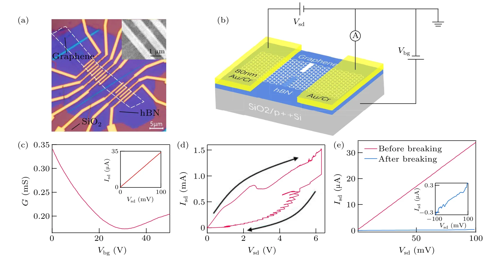
Standard electron beam lithography (EBL) and thermal evaporation of 80-nm Au/4-nm Cr metal are performed to make a graphene channel with length about 1µm(Fig.1(a)).Another EBL and O2plasma etching are carried out to get∼1.7-µm wide graphene ribbons.Before breaking process,the graphene stripe shows a linear current–bias (Isd–Vsd) response curve with a two-terminal resistance around 2.9 kΩand is p-doped with a charge neutrality point (CNP) around back voltageVbg=30 V(Fig.1(c)).

Fig.1.Schematic diagrams of a device and the feedback-controlled electromigration.(a) An optical image of an hBN-graphene stacked heterojunction device with the SiO2/Si substrate appearing in rufous,h-BN in blue,the Au/Cr electrodes in yellow,and graphene before etching in white dashed frame.The inset is a scanning electron microscope (SEM) image of this device.(b) A schematic diagram of a graphene nanoconstriction and the measurement circuit.(c)Conductance as a function of back gate voltage Vbg recorded at Vsd=100 mV before breaking.The inset is a current–bias(Isd–Vsd)linear response curve.(d)Isd–Vsd traces recorded during feedback-controlled electromigration process.The bias voltage sweeping routine is shown as black curves with arrows.(e)Current traces as a function of Vsd before and after breaking shown in red and blue.
Then feedback-controlled electromigration process is performed to achieve nanoconstrictions determined by the setting resistance threshold,at room temperature in air.We ramp up the direct current (dc) voltage between source and drain electrodes while monitoring the current with a 5-kHz sampling rate.At a critical current density,the graphene structure would break and fail,resulting in a resistance increase.Applied voltage will automatically decrease when sample resistance increases by 10%and ramps up again until the target resistance threshold 0.3 MΩ is reached (Fig.1(d)).After breaking, theIsd–Vsdcurve deviates from Ohmic response (Fig.1(e)).The resistance threshold is two orders of magnitude larger than before breaking, but several orders smaller than that in completely breaking graphene nanogaps,[30,31]which preliminarily indicates formation of a nanoconstriction.
2.2.Electronic measurements
Transport investigations are performed in our helium-III refrigerator (Oxford instrument) with a base temperature of 260 mK.Differential conductance (dI/dV) against bias and gate voltages (Vsd&Vbg) of as made nanoconstriction is measured by standard lock-in technique (Stanford Research SR830) through a data acquisition board (National Instruments,PCI 6289)together with a LabVIEW program.A lownoise current amplifier (DL instrument 1211) is used to convert current to voltage.
3.Results and discussion
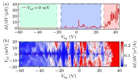
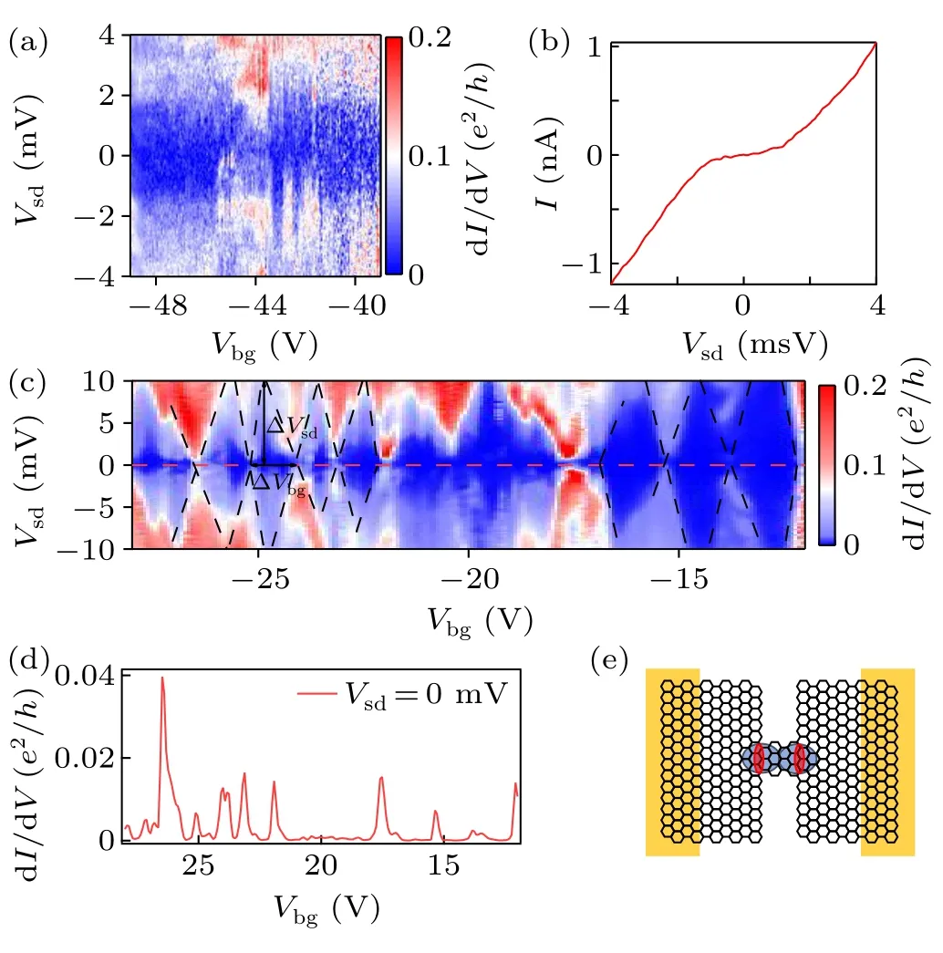
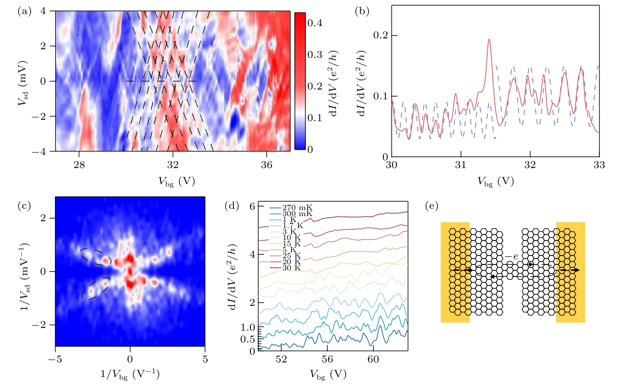
A gate voltage which applies a vertical electrical field to our nanoconstriction structure is swept from−60 V to 45 V while DC bias voltage between source and drain electrodes is kept at zero volt.As gate voltageVbgincreases from−60 V to 40 V, dI/dVexhibits remarkable changes by 20 times,0.02e2/h(e, the electron charge;h, Planck’s constant) atVbg=−60 V to 0.43e2/hat 40 V (Fig.2(a)).A clear distinction of gate depends is observed.dI/dVhas a very small value(around 20 nS)and remains unchanged when gate voltageVbgis−60 V To understand these distinct electron transport behaviors in a single device, we measure dI/dVas a function of gate and bias voltages,VbgandVsd(Fig.2(b)).Three types of transport behaviors are reproduced (marked by dashed rectangles)in these measurements and a crossover in three transport patterns is found.dI/dVshows negligible value of conductance with weak fluctuation in the regime−60 V Fig.2.Electron transport spectra of a graphene nanoconstriction.(a)Trace of Vbg dependence of differential conductance (dI/dV) at Vsd =0 mV,in which three regions are shown as light green,light blue,and rosered rectangles.(b)False color image of dI/dV as a function of Vsd and Vbg.Three different transport regions, tunneling-like region, Coulomb blockade region, and electron interference region are shown by dashed boxes corresponding to those in panel (a), respectively.The horizontal red dashed line is corresponding to trace in panel(a). In the first region,the transport behavior is characterized by a tunneling-like nonlinearIsd–Vsdresponse curve but with much larger current than that in a typical graphene nanogap[30](Fig.3(b)).Besides,figure 3(a)shows dI/dVplots as a function ofVbgandVsd, exhibiting negligible back gate response similar to that in previous nanogaps work,[23]despite some random non-producible high conduction sections with a typical value of 0.5 µS which may be attributed to instability of our graphene nanoconstriction.[29]The low conductance and lack of gate control in this region indicate the nanoconstriction forms a non-transmissive region to electrons.A directly tunneling process occurs in a finite high and nanometer wide barrier in the nanoconstriction,as shown in Fig.3(e). In the second region,a more detailed measurement is performed inVbg(−28 V Information about the nanoconstriction can be directly achieved by using Coulomb blockade theory.The charge addition energyEaddwhich is an important quantity to estimate the sizes of quantum dots,is obtained from the height of each diamond ∆Vsd(4 meV to 20 meV).Eadd=e2/Ctotal+∆E ≈e2/Ctotal=αe2/CG, when energy spacing ∆Eis negligible,whereCG(Ctotal) is capacity between nanoconstriction and gate(surroundings)andα=CG/Ctotalis called the lever arm equaling to the ratio of ∆Vsd/∆Vbg.We obtain a rough estimate for the size of the graphene nanoconstriction by modeling nanoconstriction area as a circular plate capacitor withε0is the vacuum permittivity,tandεbgare the thickness and the relative dielectric constant of the back gate dielectric layer, respectively.Finally, we havet/εbg∼81.92 nm and extractα ∼6.7×10⁻³, yieldingd ∼28 nm–59 nm,comparable to those in other works.[18,22] Above analysis indicates that in the second region, this nanoconstriction behaves like an electron island entrapped by two tunneling barriers to graphene leads in which the extension area of electrons is formed other than the scenario in the first region(Fig.3(e)). Fig.3.Directly tunneling through a barrier and Coulomb blockade regions.(a) Plots of dI/dV as a function of Vsd and Vbg from −49 V to−39 V.(b) Isd–Vsd response curve in panel (a).(c) Plots of dI/dV as a function of Vsd and Vbg from −28 V to −12 V.Several blue diamonds are denoted as crossing dashed lines.Addition energy Eadd=∆Vsd and level arm α=∆Vsd/∆Vbg are extracted from diamonds marked by arrows.The horizontal red dashed line corresponds to trace in panel (d).(d) Trace of Vbg dependence of dI/dV at Vsd =0 mV.(e) Schematic diagram of changes in barriers of the two transport regions.Blue and red ovals represent barriers in lower and higher gate ranges,respectively.And scope of delocalized electrons in the nanoconstriction gets larger as Vbg increases,shown as the portion between two barriers of the same color. Figure 4(a)shows electron transport behavior in the third and most conductive region, exhibiting a checkerboard pattern in the dI/dVfalse color map as a function of gate(27 V In this region, electron mean free path is comparable to or larger than sample sizes.Further,the ratio of widthWand lengthLof samples determines whether it is periodic singlemode or quasi-periodic multi-mode Fabry–Perot interference.In case ofL ≪WorW →0,longitudinal modes always dominate in transport and conductance maps and fast Fourier transforms(FFTs)of them are generally with high contrast.WhileLandWturn to be comparable, longitudinal and transverse modes coexist and it exhibits quasi-periodic multimode patterns in conductance maps, resulting in smaller contrast in FFTs.Using a-particle-in-a-box approximation,we have relevant length scale formulal=hvF/(2E),wherevFis the Fermi velocity for graphene.UsingvF=1×10⁶m/s,we estimatelis about 1.8 µm–2.8 µm, slightly larger than the sizes of our graphene channels.This indicates that, in this region, height and width of barriers between graphene leads and nanoconstriction decrease to result in an increase in transmissivity so that electrons propagate in the whole channel through the nanoconstriction and then reflect off the metal–graphene contact to form interference with an enhancement of dI/dVin oscillations againstVbg,as shown in Fig.4(e). However, we cannot exclude the existence of other type of interference, such as universal conductance fluctuations(UCF).Electrons are predominantly scattered by impurities but keep coherent after several different scattering paths, resulting in interference patterns.In graphene samples, UCF oscillations are prominent near Dirac point and have a modulation on Fabry–Perot interference patterns which turns into intermediate peaks in FFTs.[34]In our case, the gate section from 27 V to 37 V, is exactly near the Dirac point of this device, with lower carrier velocity and unknown complicated edge disorders after electromigration process which may intensively scatter electrons.Therefore,UCFs may partially account for this interference pattern.[34–36] Fig.4.Electron interference in a higher back voltage region.(a)Plots of dI/dV as a function of Vsd and Vbg from 27 V to 37 V.It exhibits a checkerboard-like interference pattern,partially displayed as a dashed grid.The horizontal dashed line is corresponding to the trace in panel(b).(b)Trace of dI/dV against Vbg at zero bias.Two dashed sine curves are used to fit the trace to estimate the periodicity of oscillations.(c)Fast Fourier transform(FFT)of plots in panel(a).It has been slightly smoothed for clarity.Two dashed ovals encircle two of four diagonal petals of peak clusters,from which we can deduce the energy spacing.(d)Temperature dependence of interference.The increase in T is indicated by the color variation from blue to red.These curves are vertically offset by 0.6 e2/h for clarity.As temperature reaches 10 K, oscillations start disappearing.(e)Schematic diagram of electron interference.Black dashed curves represent the paths of one electron in the junction.Electrons reflect at the boundary of the metal–graphene contacts due to the potential barriers between them. Successful realization of three types of transport behavior and device functions in one graphene nanostructure has been achieved in this study.It opens up a new possibility of using graphene nanostructure as novel devices or a platform for quantum transport of elections.The electrical control of these behaviors is handy compared to mechanical stretching or etching devices into different shapes.Above observation infers that the practical size of the nanoconstriction that is responsible for electron transport changes with electrostatic field applied by the gate.Numerical calculations[37–39]have shown that external electrical field can change transmission probabilities in graphene nanoconstriction, consisting with other experimental works.[17,18]Our gate-controlled modulation thus can be tribute to the following mechanism.Increase of gate voltage results in Fermi level rising in the nanoconstriction,leading to a decrease of height and width of energy barriers between the nanoconstriction and graphene leads.This changing of energy profile in nanoconstriction device in turn results in an enlargement of valid area in nanoconstriction to couple to electrode and an increase of transmissivity of electrons through barriers.Thus,dominating factors governing the electron transport change in three regimes in different gate regions,shown as a crossover in conductance maps. In summary, a crossover in transport regimes spanning from directly tunneling through a barrier with almost localized electrons in nanoconstriction, to Coulomb blockade of graphene quantum dots of∼101nm,then to electron interference through nanoconstriction in the whole graphene channel of∼1 µm, is observed in our nanoconstriction device tuned by a single back gate.The transport mechanism changes from particle picture to electron wave picture in single device due to gate dependent energy profile inside the constriction area.Such a system can play as the simplest, crucial, and fundamental building blocks in future electric devices.Although a well-defined quantum dot is not formed in nanoconstrictions prepared by electromigration due to the random local configuration with edge defects and tunable barriers,we can improve this by preparing graphene being encapsulated by two hBN flakes and etched into small constrictions by plasma,then being electro-burned in pure oxygen atmosphere, and undergoing longtime current cycles for stableness finally.Furthermore,benefiting from two large areas of graphene leads which can be tuned in a well-designed gate structure separately from nanoconstriction,we anticipate this platform will have further benefits in developing novel electronics and spintronics. Acknowledgments Project supported by the National Basic Research Program of China (Grant No.2016YFA0200800), the Strategic Priority Research Program of the Chinese Academy of Sciences (Grant Nos.XDB30000000 and XDB07030100), and the Sinopec Innovation Scheme(Grant No.A-527).
3.1.Tunneling-like transport
3.2.Coulomb blockade

3.3.Electron interference

4.Conclusion and perspectives
杂志排行
Chinese Physics B的其它文章
- Interaction solutions and localized waves to the(2+1)-dimensional Hirota–Satsuma–Ito equation with variable coefficient
- Soliton propagation for a coupled Schr¨odinger equation describing Rossby waves
- Angle robust transmitted plasmonic colors with different surroundings utilizing localized surface plasmon resonance
- Rapid stabilization of stochastic quantum systems in a unified framework
- An improved ISR-WV rumor propagation model based on multichannels with time delay and pulse vaccination
- Quantum homomorphic broadcast multi-signature based on homomorphic aggregation
