Research on eigenstate current control technology of Flashbased FPGA
2022-12-09YueerShanZhengzhouCaoandGuozhuLiu
Yueer Shan, Zhengzhou Cao, , and Guozhu Liu
1East Technologies, Inc. Wuxi, Wuxi 214072, China
2China Electronics Technology Group Corporation No. 58 Research Institute, Wuxi 214072, China
Abstract: To solve the Flash-based FPGA in the manufacturing process, the ion implantation process will bring electrons into the floating gate of the P-channel Flash cell so that the Flash switch is in a weak conduction state, resulting in the Flash-based FPGA eigenstate current problem. In this paper, the mechanism of its generation is analyzed, and four methods are used including ultraviolet light erasing, high-temperature baking, X-ray irradiation, and circuit logic control. A comparison of these four methods can identify the circuit design by using circuit logic to control the path of the power supply that is the most suitable and reliable method to solve the Flash-based FPGA eigenstate current problem. By this method, the power-on current of 3.5 million Flash-based FPGA can be reduced to less than 0.3 A, and the chip can start normally. The function and performance of the chip can then be further tested and evaluated, which is one of the key technologies for developing Flash-based FPGA.
Key words: Flash-based FPGA; threshold voltage; eigenstate current
1. Introduction
Based on the programmable wiring switch matrix composed of Flash cells, Flash-based FPGA selects different signal paths to realize the user logical functions[1]. Because a Flash cell is a non-volatile storage[2], the information will not be lost after the circuit is powered off. Therefore, Flash-based FPGA has a fast start-up speed and the circuit can quickly enter the working state after power-on, which is widely used in the field of signal processing and control. There are two types of Flash cell that can realize a Flash switch. The first is the Flash cell using N-channel, such as the A3PE series Flashbased FPGA developed by Actel Corporation. The second is the Flash cell using P-channel, such as Flash-based FPGA in this paper, both of which have their own advantages. An Nchannel Flash cell has the advantage of large driving capacity, while a P-channel Flash cell is superior to N-channel Flash cell in radiation resistance, especially in total ionization dose resistance. Therefore, Flash-based FPGA designed by Pchannel Flash cell is suitable for application in aerospace environments.
However, during the manufacturing process of a Flashbased chip, a small number of electrons or holes will be brought into the floating gate of Flash cell. The residual negative charge inside will make the P-channel Flash cell be in a state of intrinsic weak conduction, while the positive charge will make the N-channel Flash cell be in the state of intrinsic weak conduction. There is aboutμA conduction current between the source and drain of each Flash cell. In the wiring switch matrix[3], the two signals with opposite polarity will serve as the input of the signal selector MUX, thus forming a conducting current between the two Flash cells. Flashbased FPGA has several or even tens of millions of Flash cells. Such a large number of Flash cells conduction current superimposed between source and drain can result in a very large current for first time power-on when the Flash-based FPGA chip is returned from the wafer factory. Based on the calculation of the system of equivalent gate number 3.5 million of Flash-based FPGA, there are about 2912(BL) × 7844(WL) bits Flash cells in total, and the current will reach more than 10 A.Therefore, solving this problem is one of the key core technologies in the design of Flash-based FPGA chip, and it is the premise of whether the Flash-based FPGA chip can be tested and evaluated after manufacture. It should be emphasized that Flash-based FPGAs from Xilinx and Altera companies are implemented by SIP (system in a package) or integrated with Flash IP in the chip, so this problem does not exist. Because their signal transmission switch is realized by NMOS transistor, it is still SRAM-based FPGA in essence. The gates end of the signal MUX are controlled by the opposite output signals Q and Q-bar of the SRAM, so only one signal will be on, and no collusion between different signals will be formed.
In view of the eigenstate current caused by the special application of Flash cell in Flash-based FPGA, this paper first analyzes the cause of eigenstate current, and also analyzes the method to solve this problem that is produced in Actel's Flash-based FPGA with N-channel. Then through ultraviolet light irradiation, X-ray irradiation, high-temperature baking test and circuit design to try to solve the problem of the eigenstate current, and finally combined with the test data, it is feasible to solve the problem of Flash-based FPGA eigenstate current through circuit design. In other words, using circuit logic to control the path of the power supply is the most suitable and reliable way to solve the problem of Flash-based FPGA eigenstate current.
2. Mechanism analysis of eigenstate current
The structure of Flash switch in Flash-based FPGA is called a Sense_Switch[4], as shown in Fig. 1. A sense transistor is used to realize information erasing, programming and reading functions through ports of CG, BL and BLN. Switch transistor is utilized to realize signal transmission.
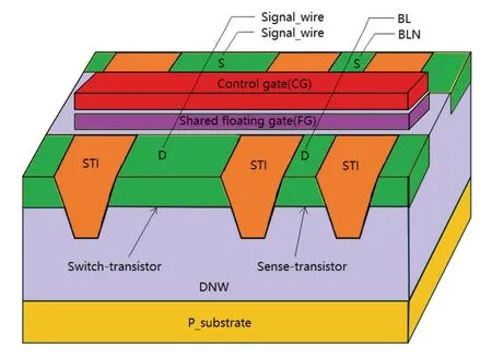
Fig. 1. (Color online) Structure of Flash switch unit.
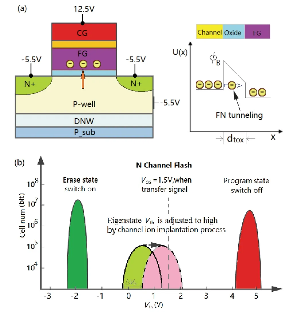
Fig. 2. (Color online) N-channel Flash. (a) Program(FN). (b) Threshold voltage distribution and adjust.
Fowler-Nordheim (FN) tunnel effect is used in programming for N-channel Flash cell. The principle and programming voltage of each port are shown in Fig. 2(a). After erasing, the threshold voltage becomes low and the switch is in the on-state. After programming, electronics enter the floating gate and the threshold voltage becomes high and the switch is in the closed state. When it works normally, it is in the state of transmitting signals, the CG terminal of Flash is 1.5 V, as shown in Fig. 2(b).
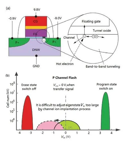
Fig. 3. (Color online) P-channel Flash. (a) Program(BTBTIHE). (b)Threshold voltage distribution and adjust.
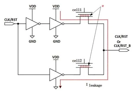
Fig. 4. (Color online) Signal selector MUX use P-channel Flash.
Band to band tunneling induced hot electron (BTBTIHE)effect is used in programming for P-channel Flash cell. The principle and programming voltage of each port are shown in Fig. 3(a). After erasing, the threshold voltage becomes low,and the switch is in the closed state. After programming, electrons enter the floating gate, the threshold voltage becomes high, and the switch is in the on-state, which is just opposite to the P-channel. When it works normally, it is in the state of transmitting signals, the CG terminal of Flash is 0 V, as shown in Fig. 3(b).
In Flash-based FPGA, CLK, RST and output signals of the logic unit are usually input to the next level as complementary signal as selection, as shown in Fig. 4. Whether N-channel or P-channel Flash-based FPGA, the intrinsic state of Flash may be in the on-state. In the manufacturing process of the chip in the wafer factory, the electron will be brought into the Flash cell floating gate to make it in a weak conduction state due to various ion implantation processes[5], which results in the formation of the leakage current from the power supply to the ground as shown in Fig. 4. The conduction state of the Flash cell in N-channel is just opposite to that in P-channel, because the holes enter the floating gate and place it in the conduction state. The difference is that more electrons enter into the floating gate of Flash cell than holes in the manufacturing process. Therefore, distribution range of eigenstate threshold voltage of P-channel Flash cell is wider than that of N-channel Flash cell, and electrons enter into the floating gate of Flash cell. The P-channel Flash cell tends to be enabled, whereas the N-channel Flash cell tends to be disenabled.
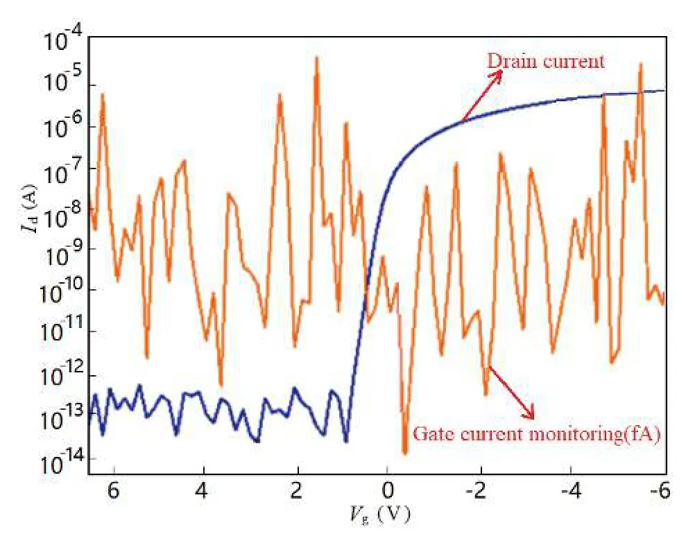
Fig. 5. (Color online) Measured eigenstate threshold voltage of the Flash switch.
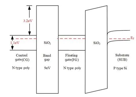
Fig. 6. (Color online) Energy band diagram of the Flash cell.
As mentioned earlier, the manufacturing process has different influences on the intrinsic threshold voltage of Flash cell in P-channel and N-channel. For the N-channel Flash cell, appropriate channel ion implantation can be used to adjust the threshold voltage of the eigenstate. In Fig. 2(b), the threshold voltage of the N-channel Flash eigenstate is adjusted to the right (toward the programming state). For P-channel Flash cell eigenstate, because the adjustment of the threshold voltage amplitude is large, if we use the same method to adjust the ion implantation, then the change of ion implantation concentration is relatively large and this may lead to changes in the breakdown voltage between the drain and the substrate. It may also lead to changes in the programming characteristics. Therefore, that the programming current becomes larger, which does not meet the requirements of high width data simultaneous programming, and needs to work closely with manufacturing process line. Thhis is difficult to operate, especially on standard Flash processes. In this paper we explore other aspects of the technology to solve the Flash-based FPGA eigenstate current problem.
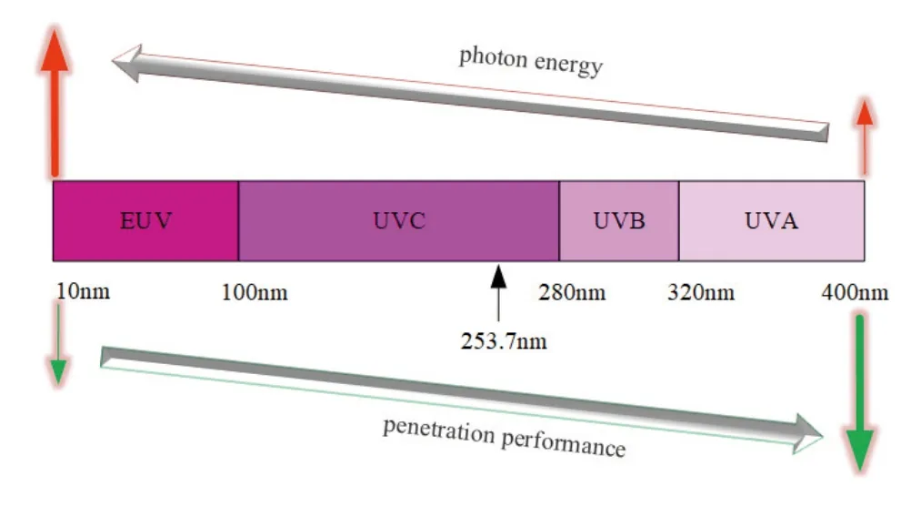
Fig. 7. (Color online) Spectrum of ultraviolet light.
The test results of eigenstate threshold voltage of Flash cell without erasing and programming after P-channel Flashbased FPGA chip returned from wafer factory are shown in Fig. 5. The initial threshold voltage is around 0 V, while the normal threshold voltage of erasing state (off state) is about-3.5 V.
3. Eigenstate current control technology
3.1. Ultraviolet light irradiation technology
Light is also a kind of wave with wave-particle duality[6],so light will also decay when it propagates in semiconductor materials; that is, light absorption is generated, and the material absorbs radiation energy, leading to electron transition from a low energy level to a higher energy level. When a certain wavelength of light hits a semiconductor material, the electrons absorb enough energy to transit from a low band to a higher band.
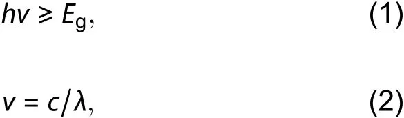
Electrons obtain energy from photons and undergo transition. The photon energy must be equal to or greater than the band gapEg. The photon energy can be obtained by Einstein-Planck photon energy formula[7,8]:
wherehis Planck's constant,vis the frequency of the photon, andcis the speed of light, as shown in Fig. 6,Egof Si is 1.1 eV, and the wavelength of the corresponding photon is about 1100 nm, which is in the visible region. The band gap between Si and SiO2isEg= 3.2 eV, and the corresponding photon wavelength is about 378 nm, which is in the ultraviolet region.
Ultraviolet light has a wavelength range from 10 to 400 nm, and ultraviolet light with a wavelength range of 100-280 nm is called UVC (C-band ultraviolet) light, as shown in Fig. 7. Ultraviolet light in this band has good penetration performance, and the photon energy is enough to excite electron transition to different semiconductor materials, which is usually used to erase ERPOM[9,10].
The corresponding photon energy in this band range is 3.45-4.97 eV, which is larger than the band gap of SiO2. Therefore, when the Flash cell is irradiated with UVC light, this part of UVC light will be absorbed by the electrons in the floating gate, making it escape from the substrate or excite to free space over the Si-SiO2interface barrier (as shown in Fig. 8). A typical method is to irradiate the chip for 45 min with a wavelength of 253.7 nm and the corresponding photon energy of 4.89 eV to complete the erasure of the Flash cell.
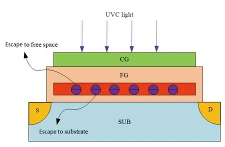
Fig. 8. (Color online) Ultraviolet light erasing.
However, in practical applications, there are some limitations in erasing Flash information with UVC light, mainly reflected in the reflection of UVC light on the metal layer and passivation layer of the chip. The metal layer is used to realize the signal transmission between logic, mainly composed of copper (Cu) or aluminum (Al). The function of the passivation layer is the electrical isolation between different metal layers and the isolation from the external environment, and the main component is silicon nitride[11]. The thickness, transmittance and reflection coefficient of the passivation layer are important parameters affecting the efficiency of UVC erasure.The thinner the thickness, the higher the transmittance and the lower the reflection coefficient, the more favorable the UVC radiation penetrates into the bottom layer of the chip and exchanges energy with the electrons in the Flash cell floating grid (FG). Because the passivation layer needs to isolate the electrical characteristics of the device, its compactness is relatively high, which is not conducive to the penetration of ultraviolet light. Meanwhile the metal layer is more reflective of ultraviolet light. Therefore, in the use of ultraviolet light erasing non-volatile storage, there are usually few metal wirings above the memory cells, and the whole chip using metal layers generally no more than 5 layers, to reduce the accumulation of the passivation layer thickness, reduce the influence of ultraviolet light erasing efficiency, and avoid residual electrons remaining in the floating gate due to insufficient UVC light intensity and time, resulting in chip failure.
As a highly integrated programmable logic device, FPGA usually leads the development of each generation of the most advanced integrated circuit technology, with more metal layers. For FPAG with 3.5 million equivalent gates, the process of 0.11μm 2P8M is adopted, and the metal layers are as high as 8 layers. Meanwhile, the Flash cells are covered with interconnect wires, as shown in Fig. 9, Flash cells are completely covered with M7 and M8 metal layers and 9 passivation layers. The thickness of the passivation layer reaches 15μm, and the UVC light cannot penetrate the Flash cell at the bottom. Even if the UVC light is irradiated for a longer time, the Flash cell cannot be erased.
Fig. 9. (Color online) Metal wiring of Flash-based FPGA.
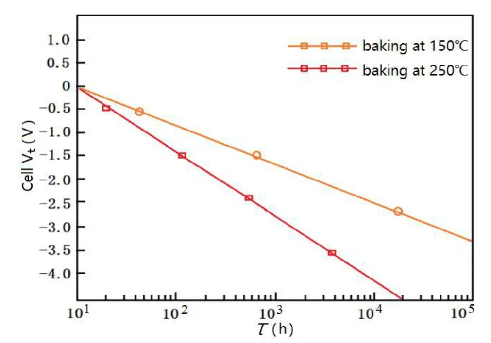
Fig. 10. (Color online) Relationship between threshold voltage drift and baking time.
3.2. High temperature baking technology
High-temperature baking was originally used to evaluate the data retention ability of Flash cell[12], and to test whether Flash cell data can be stored for a certain number of years(e.g., 10 years) at a certain temperature (e.g., 85 °C) by means of accelerated test.
Electrons in a Flash cell floating gate are wrapped by tunnel oxide (TO) and inter poly dielectric layer (IPD). Even at normal temperature, electron leakage occurs, and the number of electrons escaping is about 2-3[13]. In 1889, Arrhenius studied the influence of acidity on the conversion of sucrose into fructose and glucose at different temperatures, and many reactions follow such rules, based on which he proposed the famous Arrhenius formula[14]. The electrons in the Flash cell float grid also obey the Arrhenius law at high temperature and conform to the exponential model. In other words, the logarithm of data holding time at different temperatures is linear with the reciprocal of temperature. Therefore, the escape of electrons can be accelerated through high-temperature baking, and the Flash cell can be erased theoretically through high-temperature baking test.
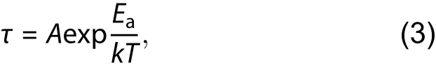
whereτis time,Ais constant,Eais thermal activation energy,kis Boltzmann constant andTis absolute temperature. The thermal activation energy of Flash cells varies widely from 0.3 to 1.9 eV, so the time required for Flash cells with different thermal activation energy to accelerate electron escape through high-temperature baking varies greatly, increasing exponentially.
(1) For thermal activation energyEa= 1.0 eV, baking time at different temperatures can be calculated:
The data retention time is 10 years at 85 °C and the baking time is 600 h at 150 °C;
The data retention time at 85 °C is 10 years, and the baking time is 3 h at 250 °C;
(2) For the thermal activation energyEa= 0.3 eV, the baking time at different temperatures can be calculated:
The data retention time is 10 years at 85 °C and the baking time is 3.8 years at 150 °C;
The data retention time at 85 °C is 10 years, and the baking time is 173 days at 250 °C.
Therefore, for the Flash cell with low thermal activation energy, it is unrealistic to erase the Flash cell by baking at high temperature to remove the electrons in the floating gate, so as to shift the threshold voltage of the Flash cell from the eigenstate of 0 V to the erased state of -3.5 V. For Flash cells with 0.3 eV thermal activation energy to bake at 250 °C at high temperature, the relationship between threshold voltage drift and time is shown in Fig. 10. It takes nearly 10 000 h to complete the erasure of Flash cells.
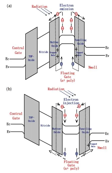
Fig. 11. (Color online) Energy band diagram of floating gate structure under X-ray radiation ionization. (a) Programming state. (b) Erasing state.
3.3. X-ray irradiation technology
Physical mechanisms for high-energy photons or ions to interact with target materials include Compton effect and photoelectric effect[15-20]. The X-ray radiation ionization effect is mainly the photoelectric effect of photons interacting with inner electrons. According to the principle of energy and momentum conservation, the photoelectric effect mainly occurs in layer K. The expressions of non-relativistic effect and relativistic effect are shown in Eqs. (4) and (5) respectively[15-20]:
whereσKis the photoelectric cross section of K layer;αis fine structure constant;m0c2is the rest energy of the electron;hvis the energy of X-ray photons;σThis 6.65 × 10⁻²⁵cm2.
During irradiation, the interaction of photons with electrons in the outer layers of atoms produces a large number of electron-hole pairs. In the uncompounded electron-hole pair, the electrons in the electron-hole pair are removed by the electric field, and the remaining holes affect the electrical properties of the system in the form of oxide charge and interfacial states. The photoelectric effect is considered from the types of elements and the energy of the irradiation source. For different types of elements, because the photoelectric cross section (σK) of the outer atom K layer is proportional to the fifth power of the atomic number (Z5), the probability of the atomic photoelectric effect is greater with the increase ofZ. When X-ray passes through the interface formed by highZmaterial and lowZmaterial, the absorption dose of highZmaterial is higher than that of lowZmaterial. The photoelectrons generated by highZmaterial will enter SiO2and generate electron-hole pair. The uncompounded electronhole pair will generate oxide charge and interface state under the electric field. At the same time, when X-ray passes through Si and SiO2, because the average atomic weight of Si and SiO2is not uniform, Si absorption is greater than SiO2, consequently, after electrons move to SiO2to deposit energy,dose enhancement will occur near the interface of the device. Because optical absorption is closely related to the atomic number, resulting in poor uniformity of optical absorption, X-ray radiation ionization effect will have a dose enhancement effect[15-20].
For a pFLASH type sense-switch device, its X-ray radiation ionization effect is related to its programmed or erased state. That is, its radiation mechanism is mainly manifested as: programmed state: electron emission and erased state: electron injection. The specific irradiation mechanism is shown in Fig. 11[20-24].
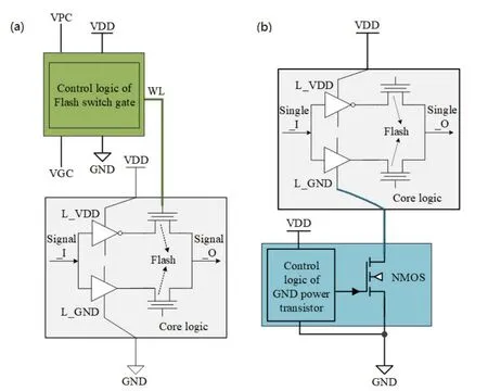
Fig. 12. (Color online) Two logic control schemes for the first poweron. (a) Control the Flash gate. (b) Control the GND of core logic.
Therefore, the change of threshold voltage (ΔVTH) mainly depends on the gain and loss of floating gate charge at T1 and T2 due to light emission, interface traps and electron/hole pairs caused by oxide between tunnel oxide and control gate/floating gate. ΔVTHcan be expressed in Eq.(6)[20,23,24].
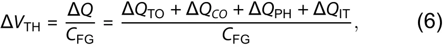
where ΔVTHis the change of threshold voltage, ΔQis the change of total charge of floating gate,CFGis the capacitance between floating gate and substrate (N-well), ΔQTOand ΔQCOare the charge loss in tunnel oxide and control gate oxide respectively, ΔQPHis the charge loss caused by light emission, ΔQITis the interface trap charge.
3.4. Circuit logic control technology
Circuit logic control is from the perspective of circuit design, adding the control logic for the first circuit power-on on the Flash-based FPGA chip to prevent the leakage flow from the power supply VDD to ground GND. In addition, the control logic has the memory function. After the Flash cells are erased and powered on again, the VDD power supply can be normally powered on. Therefore, the normal operation of the chip will not be affected.
There are two main schemes to control the formation of the chip's first power-on large current through circuit logic,as shown in Fig. 12. The first scheme is to increase the control logic in the Flash cell gate. When the chip is powered on for the first time, the Flash cell gates are supplied with high voltage and the Flash switch units are closed, thus preventing the formation of the power supply VDD to ground GND current. The second solution is to add ground power transistors in the path of GND to control ground GND when the chip is powered on for the first time and make it closed, which also prevents the formation of power supply VDD to ground GND current.
Next, according to the two schemes in Fig.12, specific circuits are designed to analyze and compare the feasibility. The circuit design for the first scheme to control the Flash cell gate voltage is shown in the upper right corner of Fig. 13,which is mainly composed of CTL and transistor P4. CTL is the control logic, VLS is the voltage level shift circuit, and P4 is the pull-up drive circuit of the PMOS transistor. The signal Fst_puc with high level VDD is generated during the first power-on test after chip return from the wafer factory, and signal ENB with high level VPC is output after level conversion through VLS module to shut down PMOS transistor P4. The purpose of converting the signal Fst_puc from the voltage range VDD-GND to the voltage range VPC-VGC to control the transistor P4, rather than directly control it, is to prevent collusion between power supplies in various states.
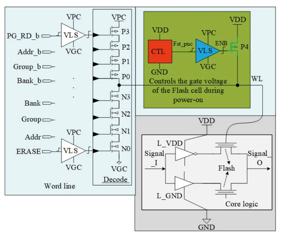
Fig. 13. (Color online) Voltage control of Flash cell gate.
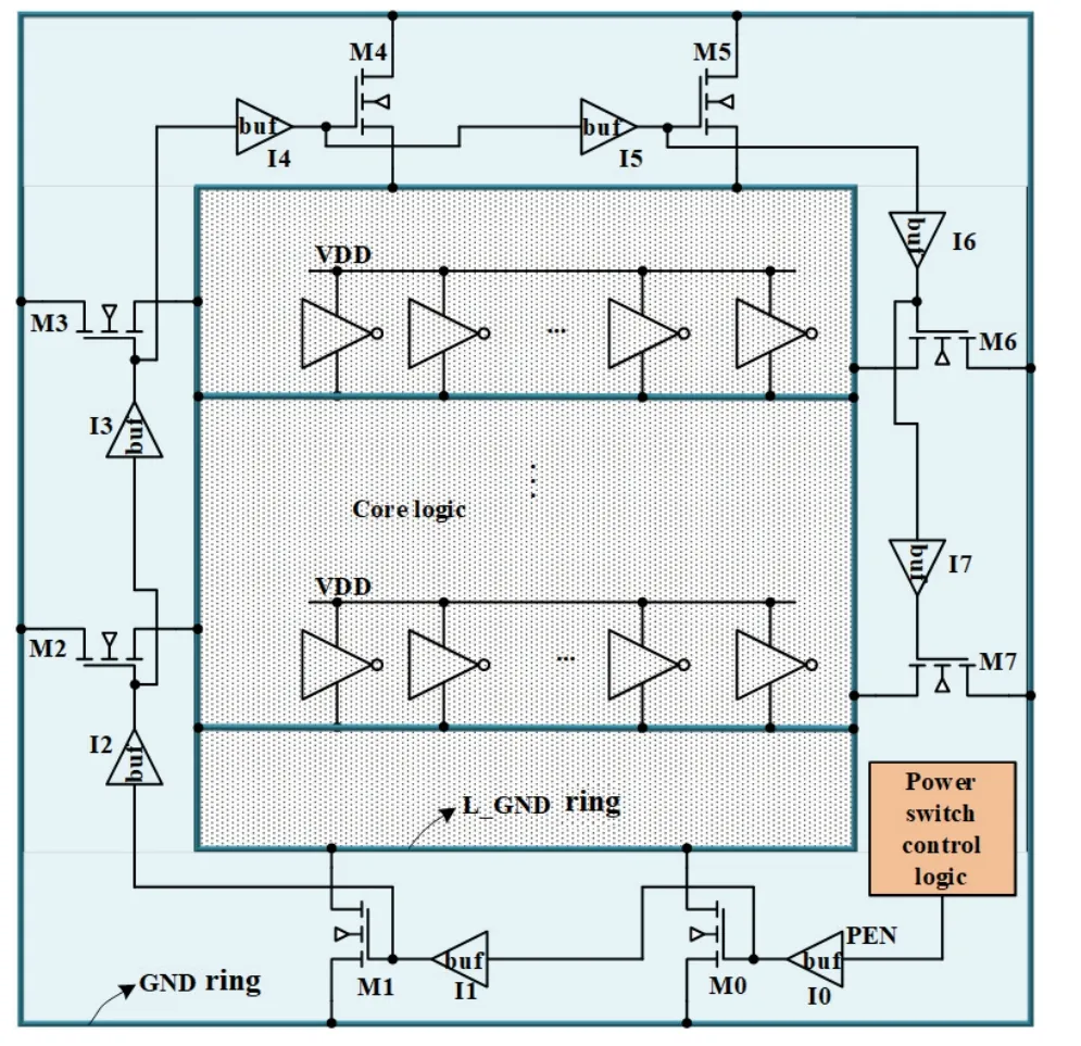
Fig. 14. (Color online) GND to L_GND channel.
The specific design of the second scheme is shown in Figs. 14 and 15. In Fig. 14, ground channels are formed around the chip, and NMOS transistors are added between external pin GND and core logic L_GND as the power transistors of ground. Fig. 15 is power transistors control logic composed of Flash cells (P0-P7) for memory function, which is a concrete implementation of the power switch control logic in Fig. 14. When the chip is powered on for the first time after the chip is returned from the wafer factory, the channel of core logic L_GND is closed to place it in the suspended state,thus preventing the generation of large core current.
After the circuit is successfully powered on, we first erase the Flash cells in the Flash-based FPGA, and then execute the special erase instruction to erase the Flash cells as the pulldown transistors in Fig. 15 through MP0 and MN0 input high voltage, and close the Flash cells of the pull-down transistors.When the chip is powered on again, we pull up point A to a high level through the pull-up resistor MP1. The output control signal PEN is at high level, and the core logic L_GND channel can be normally turned on. It should be noted that due to different batches, the eigenstate threshold voltage of Flash cells will be different, so the number of Flash cells in the pulldown circuit composed of Flash cells must be enough to ensure that point A in Fig. 15 can be pulled down to low level and the output control signal PEN is at low level.
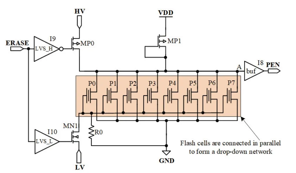
Fig. 15. (Color online) Control logic of L_GND channel switch.
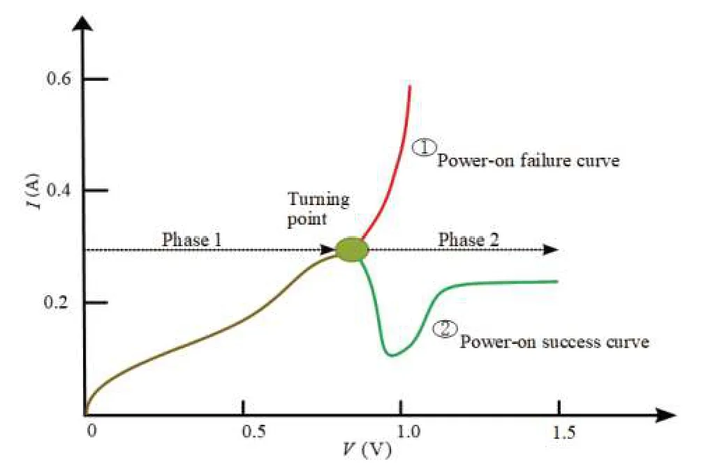
Fig. 16. (Color online) Competition between voltage and current during power-on.
In fact, voltage and current compete during VDD poweron (as shown in Fig. 16). At the beginning of the power-on process, due to the control signal in an uncertain state and signal transmission delay, the current increases at the same time when the VDD voltage increases, and this current will hinder the VDD voltage elevation. When the VDD voltage reaches a certain point, the control signal can turn off the current on the Flash cells. In this case, the up voltage drops sharply to further increase the voltage, and the circuit is powered on.
The disadvantages are obvious for the first option. As can be seen from the Fig. 13, CTL control logic and core logic is the same power VDD, which is the core power supply for the chip, the control signal need to be converted through voltage level shift module VLS[25], and the working voltage of voltage level shift module VPC and VGC on power-on moment cannot complete a reasonable offset, and the VLS will produce a lot of delay and even may not work normally. In addition, as Flash cells are distributed in the whole chip, the delay of the word line is also relatively large, so the pull up transistors P4 of the word line cannot be opened in time to set the word line to high level at the moment of power-on,and the Flash switching units are still on to form a large current, which ultimately leads to the failure of power-on, as shown in curve ① in Fig. 16. The second scheme has obvious advantages, the NMOS can be shut down in a relatively short time by using a large driver with relatively high driving capacity around the chip, as shown in curve ② in Fig. 16.
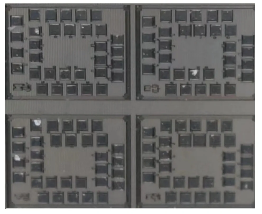
Fig. 17. Flash cell PCM.
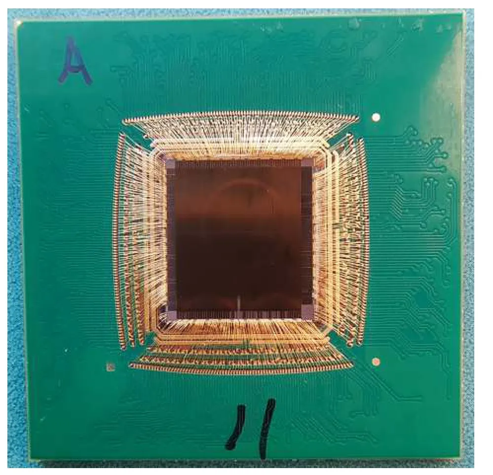
Fig. 18. (Color online) A 3.5 million Flash-based FPGA.
The circuit design control technology with controlling the path of power supply to solve the Flash-based FPGA eigenstate current problem as shown in Fig. 14 is adopted in 3.5 million Flash-based FPGA. To prove the effect of the proposed method, a Flash-based FPGA without the proposed method is also designed for comparison.
4. Experimental results and analysis
UVC irradiation, X-ray irradiation and high-temperature baking tests were carried out on Flash cells used for PCM monitoring (see Fig. 17) and 3.5 million Flash-based FPGA (see Fig. 18). Finally, the Flash-based FPGA that uses circuit design to control the eigenstate current is tested. Fig. 17 shows a single Flash switch, which is mainly used to test its performance in detail and is applied in 3.5 million Flash-based FPGA.
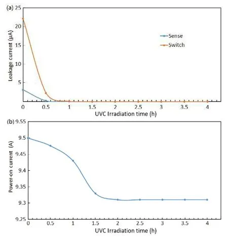
Fig. 19. (Color online) UVC irradiation test. (a) Flash cell PCM. (b) Flashbased FPGA.
There are four groups of circuits. The first three groups are the combination of Flash cell PCM and Flash-based FPGA,the fourth group is Flash-based FPGA without controlling the eigenstate current and five Flash-based FPGAs with circuit design to control the eigenstate current.
First, the first group of circuits (Flash cell PCM and Flashbased FPGA) was irradiated by ultraviolet light with a wavelength of 253.7 nm, and the photon intensity was about 30 mW/cm2.
For the Flash cell that is not covered by a metal layer, the effect of eraser can be achieved by UVC light irradiation. Initial 0.5 h irradiation can erase most electrons, and the saturation state is almost reached after 1 h. The results of 2 and 4 h of irradiation are basically the same, and the threshold values of sense transistor and switch transistor remain basically unchanged as shown in Fig. 19(a). The leakage level is mainly reflected in the switch transistor, about a few nA. However,for 3.5 million Flash-based FPGA, there is no significant change in the on-current after 4 h of UVC light exposure as shown in Fig. 19(b).
Second, the second group of circuits (Flash cell PCM and Flash-based FPGA) was irradiated by X-ray at a dose rate of 50 rad (Si)/s.
For the element with positive initial threshold and large leakage, X-ray irradiation can erase the element to a negative state to a certain extent and reduce leakage. With the increase of radiation dose, the threshold has a further negative drift and leakage is further reduced. At 150 krad, the leakage of Flash unit can be limited to less than 10μA as shown in Fig. 20(a). However, for 3.5 million Flash-type FPGA, the on-current still has no obvious change after X-ray irradiation, and remains above 8 A as shown in Fig. 20(b).
The third group of circuits (Flash cell PCM + Flash-based FPGA) were subjected to 168 h of superimposed high-temperature baking test at 150, 200 and 250 °C, respectively.
High-temperature baking can reduce initial state threshold and leakage level of Flash unit, but there is no order of magnitude change, the effect is far less than X-ray and UVC irradiation as shown in Fig. 21(a). For 3.5 million Flashbased FPGA, the on-current is almost unchanged after the high-temperature baking test as shown in Fig. 21(b).
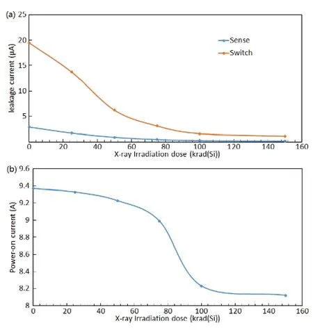
Fig. 20. (Color online) X-ray irradiation test. (a) Flash cell PCM. (b)Flash-based FPGA.
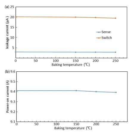
Fig. 21. (Color online) High temperature baking test. (a) Flash cell PCM. (b) Flash-based FPGA.
Finally, the first power-on waveform of the circuit without path control of power supply (shown in Fig. 22(a))was compared with the circuit with path control of power supply (shown in Fig. 22(b)) at 25 °C. The core current is 9.3794 A and the core voltage is 1.4993 V on the circuit without path control of power supply. The peak core current at first poweron of the circuit with path control of power supply is 136.1 and 77.8 mA after stabilization. At this time, the core voltage reaches the set value of 1.5002 V.
Five Flash-based FPGAs with path control of power supply to control the eigenstate current are tested and the statistical results at three temperatures (-55, 25, 125 °C) are shown in Fig. 23.
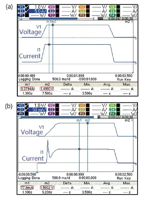
Fig. 22. (Color online) Power-on waveform. (a) Circuit without path control of power supply. (b) Circuit with path control of power supply.
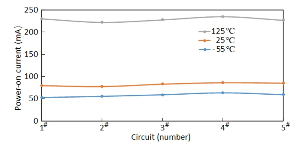
Fig. 23. (Color online) Power-on current of the circuit with path control of power supply at -55, 25 and 125 °C.
Through these test results, to remove the electrons in the Flash floating gate, it can be seen that the effect of hightemperature baking is the worst and it takes a long time. UVC irradiation can obviously remove the electrons in the floating gate of a single Flash cell, but the effect of UVC irradiation on Flash-based FPGA is also not obvious because the metal layers and passivation layers are covered on the Flashbased FPGA. X-ray irradiation can reduce the leakage current of Flash cell, but is not enough to reduce the power-on current of Flash-based FPGA to an acceptable range. Through the circuit logic control of the core L_GND channel to solve the power-on large current caused by Flash cell eigenstate achieved obvious effect. In addition, considering the cost, the circuit design to control the power-on current increases the chip area by about 10%, thus increasing the cost of the chip.A comparison of the above four methods in terms of leakage current of Flash cell, power-on current of Flash-based FPGA,time consumption, and cost is shown in Table 1.
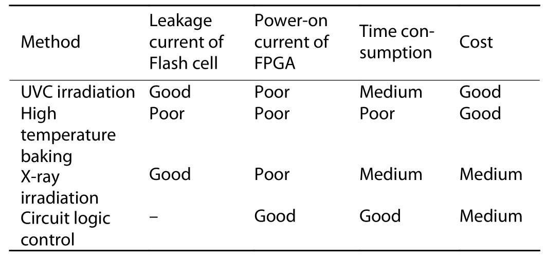
Table 1. Comparison of four methods.
5. Conclusion
In this paper four methods are used to solve the eigenstate current problem of Flash-based FPGA. Finally, the meth-od of circuit logic control power supply path is applied to 3.5 million Flash-based FPGA. Through the field measurement of the chip return from the wafer factory, 3.5 million Flash-based FPGA with path control of power supply can be successfully powered on, and the power current drops from the value nearly 10 A of the Flash-based FPGA without path control of power supply to below 0.3 A, which enables the Flash-based FPGA to smoothly enter the stage of function and performance evaluation. For further research on the eigenstate current control technology of P-channel Flash-based FPGA, on the one hand, it may be solved by circuit design, and on the other hand, it may be developed from the independent Flash process line. In the manufacturing process, ultraviolet light is irradiated many times to eliminate the electrons in the floating gate.
Acknowledgements
This work was supported by the National Natural Science Foundation of China (No.62174150) and the Natural Science Foundation of Jiangsu Province (No. BK20211040).
杂志排行

Journal of Semiconductors的其它文章
- Humidity sensor based on BiOBr synthesized under ambient condition
- Influence of architecture and temperature of alkali atom vapor cells on absorption spectra
- A 4H-SiC semi-super-junction shielded trench MOSFET: p-pillar is grounded to optimize the electric field characteristics
- Discrimination of dislocations in 4H-SiC by inclination angles of molten-alkali etched pits
- Emitter layer optimization in heterojunction bifacial silicon solar cells
- Highly stable Ga-doped ZnO/polystyrene nanocomposite film with narrow-band cyan emission