A new nano-scale surface marking technique for the deformation analysis of Mg-based alloys
2022-10-24HungXuTngNie
Y.H.Hung ,S.W.Xu ,W.N.Tng ,J.F.Nie,*
aDepartment of Materials Science and Engineering,Monash University,Victoria 3800,Australia
b Automotive Steel Research Institute,Research Institute (R&D Centre),Baowu Iron &Steel Co.Ltd.,Shanghai 201900,China
Abstract In this work a new nanoscale surface marking technique,namely electron beam damage induced surface marking (EBDISM),is developed and tested for the first time on a fine-grained pure Mg surface.This technique utilizes focused high-energy electron beam of a scanning electron microscope to “burn” dense arrays of nano-scale grid patterns on the sample surface,and it is proved to be very effective for identifying and measuring localised deformation behaviours.However,the surface marking deposited by EBDISM is not permanent and it tends to deteriorate overtime.Cheap,easy to use and versatile,the EBDISM technique has a huge potential for quantitative measurement of strain field and nano-scale deformation analysis.
Keywords: Magnesium alloy;Fine grain structure;Deformation analysis;Surface patterning;Deformation field.
1.Introduction
Although Mg and most of its alloys are considered to have poor room temperature ductility,recent discoveries have showed that Mg can also be super-formable when its grain size is sufficiently small (close to 1 μm),thanks to the significantly increased activities of grain boundary sliding and dynamic recrystallization [1].Considerable interests have grown recently in studying the deformation mechanisms of finegrained Mg-based alloys [2–8].However,it is very challenging to characterise the deformation mechanisms in the finegrained Mg alloys,because a great portion of deformation activities is highly localised at grain boundaries (e.g.grain boundary sliding) [9],which are difficult to identify,track and measure by conventional optical and scanning electron microscopy.It is also difficult to use conventional electron back-scattered diffraction (EBSD) to analyse the localised deformation,since EBSD mapping cannot obtain quality diffraction signal at grain boundaries and heavily deformed regions[10–12].
Surface marking is an important method for distinguishing localised deformation and measuring macroscopic in-plane displacement of a deformed sample surface [13,14].It is done by depositing highly distinguishable surface marks (random paint speckles,dots or patterns) on a flat sample surface before deformation,then based on the geometrical changes of the surface marking after the plastic deformation,the localised deformation on the sample surface can be distinguished and quantified[15].However,since the traditional surface marking method involves printing with inks,pigments or engraving the surface mechanically,the scale of the marking result is usually too large (from 1 mm to 100 μm) and not suitable for nanoscale deformation analysis [16].Very recently,advanced surface marking techniques such as gold nano particle sputtering and photo/e-beam lithography are developed for nano-scale deformation analysis,which can achieve a surface resolution of~10 nm [17–20].However,these techniques involve the use of specialised equipment and consumables to mark the sample surface,making it expensive,complicated and time consuming for sample preparation.Therefore,a cheap and easy nano-scale surface marking technique is much desired for the study of plastic deformation of fine-grained Mg alloys.
In this work,we have developed a new nano-scale surface marking technique: namelyelectron beam damage induced surface marking(EBDISM),which uses a focused electron beam in a scanning electron microscopy(SEM)to“burn”visible marks on the polished Mg sample surface.The working principle of this surface marking technique is inspired by a commonly seen phenomenon called “beam damage” in SEM operations,that the area of the observation tend to gradually change contrast (become darker or brighter) over time under continuous exposure to the high-energy electron beam.This new technique can quickly and cheaply create an extremely dense array of highly distinguishable marking points on polished Mg sample surface by only using a standard SEM and EBSD.
2.Materials and methods
The sample tested for surface marking in this work are cut from fine-grained pure-Mg sheets (grain size~4 μm) that are produced by severe plastic deformation (low-temperature extrusion and subsequent high strain-rate rolling).The thin sheets were cut into strips along the rolling direction (RD)with a dimension of 50 mm × 5 mm × 1 mm,the side(cross-section parallel to RD and ND) of these strips were then metallographically prepared using SiC papers and subsequently polished by 50 nm diameter silica suspension.
The marking and subsequent SEM characterisation was performed on JEOL 7001F scanning electron microscope equipped with EBSD detector of OXFORD instruments.Controlled by SEM operating software and the AZtec EBSD software by OXFORD instruments,the electron beam automatically marks an array of points (one point at a time).The electron beam accelerating voltage was set to be 30 kV,and the beam current~14 nA.For each marking point,the exposure time was set to be 20–50 ms to ensure sufficient beam damage for sharp marking result.After surface marking,10%of tensile strain was applied to the sample by a tensile test machine.
3.Results
3.1.Surface marking of EBDISM
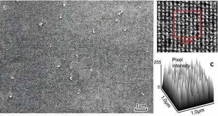
The marking result of the EBDISM is shown in Fig.1.The secondary electron(SE)image(Fig.1a)shows that dense arrays of bright marker points were deposited on the sample surface by EBDISM,and these marker points are sharp and much brighter than the surrounding area.When taking a closer look of each individual marker points (Fig.1b),it can be found that they are slightly elongated since the sample was tilted during the marking process (same as that needed for EBSD operation).The marking points are evenly distributed and have a uniform inter-spacing,forming a grid-like surface pattern.The distance between two adjacent marking points is less than 100 nm but still has plenty of inter-spacing for good point-to-point sharpness,which is enough for measuring localised deformation with nano-scale precision and accuracy.Fig.1c is the 3-dimensional graph showing the pixel intensity within the 1 μm × 1 μm sampled area,indicated by the redcolour square frame in Fig.1b.With proper image processing,the contrast of these marking points can be further enhanced for visual analysing.Since the image is an 8-bit Tiff image,there is a total of 256 level of intensity,at the centre of the marking points,the intensity can be as high as 255 while the surroundings as low as 0.Hence,this new surface marking technique yields very good special resolution and sharpness,which has great potential for applications involving computeraided digital image correlation and strain mapping.
3.2.Surface deformation analysis using EBDISM
After surface marking,10% of tensile strain was then applied to the fine-grained pure-Mg sample.Fig.2 shows a SE image of the deformed sample surface.From the SE image,deformation traces such as inter-granular cracks,twin bands,and grain boundary sliding are readily visible.With the distorted and mismatched arrays of surface marking points lying on these deformation traces,the localised surface displacement as well as tear and shear can be easily identified by visual observation.
To show how effective this new surface marking can distinguish even the tiniest localised deformation,In Fig.2b we highlighted two of the surface-marked guidelines running through the area from top to bottom.By close examination of this area,discontinuity of the guidelines can be found at the grain boundary,indicating sliding movement occurred at the grain boundary.Some slip traces can also be observed,and it is interesting to see the guidelines across through the slip traces gradually change its direction,which indicates an obvious shear deformation.In addition,a close-up of the SE image of twin band is shown in Fig.2c,and by drawing marked guidelines across through the twin band,it can be seen that the guidelines abruptly change their directions after they have entered the twin band and change back to their original directions when they exit the twin band.Such guideline direction change indicates the shear deformation are accommodated by the formation of twin band:the wider the twin band,the more shear strain can be accommodated,which explains why twin bands tend to grow wider as deformation continues.
3.3.Image quality deterioration of EBDISM

Fig.1.Electron beam damage induced surface marking on polished fine-grained pure-Mg surface.(a) Secondary electron (SE) image showing the surface marking grids (b) zoomed in SE image showing the array of each individual marking points.(c) The pixel intensity 3-dimensional chart within the square of 1 μm × 1 μm (marked by the red-colour square frame in (b)).
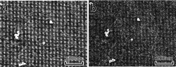
Although the newly developed EBDISM technique is a very effective method for surface marking and nano-scale deformation analysis,it has a drawback that the quality (sharpness of the marking point) of the EBDISM can gradually deteriorate over time.An example is shown in Fig.3 where a fresh surface marking and its two-day-old surface marking(same area in the same sample but after two days of exposure at room temperature) are put side-by-side for the purpose of comparison.After the two days storage,the surface marking turned blurry,and it is no longer easy to identify each individual marking points.Since fine-grained Mg samples tend to form oxidation layer much faster than coarse-grained samples[21],and it is also well known that a freshly polished Mg sample generally yields better quality SEM and EBSD results than an old sample [22],such surface marking deterioration originates from the formation of new oxidation layer at the surface marking spots when exposed to air in the atmosphere,which blocks the electronic beam from penetrating the sample surface,leading to weaker secondary electron signal generation during the SEM characterisation.Therefore,to avoid such surface marking image deterioration,preservation of EBDISM treated samples (storage in vacuum or an inert-gas environment) and/or immediate deformation and characterisation to minimize air exposure are recommended.
4.Discussion
4.1.Surface marking mechanism of EBDISM
We have shown that the EBDISM technique can create high-contrast surface marking points on Mg surface.However,the detailed mechanism about how these marking points are exactly created by electron beam is still not fully understood.These highly visible surface marks are thought to be generated by the “beam damage” [23]: the material on the sample surface gets damaged by the exposure to the high energy electron beam.Since metal itself is unlikely to be damaged by electron beam due to its strong metallic bond and high conductivity (both thermal and electrical),the beam damage is most likely to originate from the surface contamination and the oxidation layer on the Mg sample surface.

Fig.2.Deformed fine-grained pure-Mg sample surface with surface marking (sample was tilted to reveal more topographical details).(a) Overview of the sample surface with area of interest (red and green rectangle).(b) Zoomed area showing grain boundary sliding,cracks and slip traces (red rectangle area in picture a).(c) Zoomed area showing twin bands and twisted surface marking (grain rectangle area in picture a).

Fig.3.SE images showing the quality deterioration of EBDISM.(a) Marking points array right after EBDISM.(b) Marking points array after 2 days of room-temperature storage.
Surface contaminations(hydrocarbons such as ethanol,polishing solvent) are not easy to be completely cleaned after sample preparation,leaving a thin film attached to the metal surface.The electron beam could break apart the molecular structure of these contaminations,forming new compounds bonding with the sample surface [23],which usually results in a dark area when observed in SEM.However,in the case of our surface marked Mg-based samples,the marking point are far brighter than the surrounding areas in SE images,indicating that these marked points generate higher number of secondary electrons when scanned in SEM.Since surface carbonization,which darkens the image,and oxidation removal,which brightens the image,have completely opposite effects,it is recommended that no organic solvent to be used during sample preparation for best marking results (to avoid surface carbonization during SEM observation).
Therefore,we suspect that the “bright dots” deposited by the EBDISM technique on the Mg sample surface are created by the removal of oxidation layer.The original oxidation layer formed on the sample surface could be thinned down by the bombardment of high current density,high energy electron beam,thus resulting in “burnt” points on the Mg surface that are brighter in the SE image.
4.2.Potential applications of EBDISM
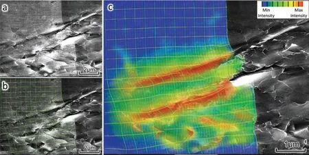
With a nano-scale pattern marking capability,the EBDISM technique can be a powerful tool for localised deformation quantification and strain field analysis.An example of utilizing the EBDISM technique for deformation analysis is presented in Fig.4,where the deformed marking pattern on a severely bent Mg sheet sample is mapped by reconstructed grid-lines (Fig.4b).Based on the distortion on each intersecting square,the extent and direction of shear,tension or compression can be intuitively obtained.Furthermore,by quantitatively measuring and calculating the distortion of each of these grids,a deformation strain field map can also be generated for more sophisticated study purposes (methods for measuring deformed grid and strain calculation are based on Ishikawa’s work [19]).

Fig.4.(a) SE image showing the cross-section of a EBDISM marked,fined-grained pure-Mg sheet sample after bending deformation,and (b) same image mapped with grid-line for easy measuring and analysis.(c) Strain filed colour map based on grid-line distortion calculation.
5.Conclusion
In summary,for the first time,a new nano-scale surface marking technique is developed by utilizing high energy electron beam in SEM and tested on fine-grained Mg samples.This technique is proved to be a very effective method for identifying and measuring subtle localised deformations (e.g.grain boundary sliding,slip traces,nano-twinning) in the study of Mg and its alloys.The sample preparation procedure for the EBDISM technique is easy (only requires simple polishing before surface marking),and the surface marking quality is surprisingly good,that a clear grid pattern consisting arrays of high-contrast marker points are deposited on the sample surface,which are highly visible in SEM observations.This new surface marking technique offers new possibilities in precise deformation quantifications (strain field analysis,slip identification and characterisation,etc.).However,it is also discovered that the surface marking created by this method is not permanent and tends to fade over time.Hence,immediate actions of deformation experiments and characterisation are highly recommended after the EBDISM.
Acknowledgements
The authors are grateful for support from the Australian Research Council (LP180100048) and Baosteel Company.Y.H.Huang wishes to acknowledge the Monash Postgraduate Award,International Postgraduate Research Scholarship,and the access of instruments and scientific and technical assistance at the Monash Centre for Electron Microscopy,a Node of Microscopy Australia.
杂志排行
Journal of Magnesium and Alloys的其它文章
- Microstructures and mechanical properties of titanium-reinforced magnesium matrix composites: Review and perspective
- Effects of deformation twins on microstructure evolution,mechanical properties and corrosion behaviors in magnesium alloys -A review
- A review of effective strides in amelioration of the biocompatibility of PEO coatings on Mg alloys
- The mechanisms of grain growth of Mg alloys: A review
- Additive friction stir deposition of AZ31B magnesium alloy
- Nonisothermal dissolution kinetics on Mg17Al12 intermetallic in Mg-Al alloys
