High-quality CdS quantum dots sensitized ZnO nanotube array films for superior photoelectrochemical performance
2022-09-24QianQianGong宫倩倩YunLongZhao赵云龙QiZhang张奇ChunYongHu胡春永TengFeiLiu刘腾飞HaiFengZhang张海峰GuangChaoYin尹广超andMeiLingSun孙美玲
Qian-Qian Gong(宫倩倩), Yun-Long Zhao(赵云龙), Qi Zhang(张奇), Chun-Yong Hu(胡春永), Teng-Fei Liu(刘腾飞),Hai-Feng Zhang(张海峰), Guang-Chao Yin(尹广超), and Mei-Ling Sun(孙美玲)
School of Physics and Optoelectronic Engineering,Shandong University of Technology,Zibo 255000,China
Keywords: ZnO nanotubes,W-doping,CdS quantum dots
1. Introduction
ZnO is a typical semiconductor material that has been widely applied in solar cells, photocatalysis, water splitting and other photoelectrochemical (PEC) fields[1-8]due to its advantages such as non-toxicity, low cost, suitable energy band position, good chemical stability and resistance to photocorrosion.[9-12]In spite of this, it must be pointed out that there are two inherent drawbacks of ZnO for its application in PEC devices. The first is the wide band gap of ZnO (Eg= 3.37 eV for wurtzite ZnO), which results in a low utilization efficiency of sunlight (only in the ultraviolet region).[13]The other problem is the relatively high recombination rate of photogenerated electron-hole pairs, which leads to a relatively low quantum efficiency.[14]Both the above drawbacks are disadvantageous for PEC performance. Therefore,ways to overcome the above drawbacks to effectively enhance the PEC performance of ZnO-based materials has always been an important research topic.
Up to now many strategies have been adopted to improve the PEC performance of ZnO-based materials, such as the nanostructure design (nanorods,[15,16]nanotubes,[17]nanofibers,[18]nanowires,[19]nanoflowers,[20]nanopowders,[21]etc.), element doping (C,[22,23]N,[24,25]Ni,[26]Na,[27]etc.),sensitization of quantum dots(QDs)with narrow band gap materials (PbS,[28]CdS,[29]CdSe,[30]etc.),and so on. Previous studies have proved that the nanostructure design and element doping can improve the PEC performance of ZnO-based materials by optimizing the light scattering paths and charge transmission paths, but these improvements are relatively limited due to the lack of any improvement in the light absorption ability.[31]Therefore, the further sensitization of QDs with narrow band gap materials is very necessary to significantly improve the PEC performance of ZnO-based materials. This is mainly due to the following points: (i) QDs with a narrow band gap can extend the light absorption range to the visible region and have better light absorption ability.(ii)The unique multiple exciton effect of QDs can effectively improve quantum efficiency. (iii) The establishment of a built-in electric field on the QD/ZnO interface can effectively promote the transport and separation of photogenerated electrons and holes. However,it is unfortunate that the PEC performance of QD/ZnO composites is still far lower than expected;this is mainly related to the poor loading quality of QDs on ZnO-based materials(low coverage ratio,local agglomeration and poor interface connection). Therefore,optimizing the loading quality of QDs on ZnO-based materials is vital for enhancing the PEC performance of QD/ZnO composites.
It is well known that the loading quality of QDs is deeply related to the surface characteristics of materials such as surface area,active sites and electronic structure.[32]Therefore,a variety of relevant strategies have been selected to optimize the surface characteristics of ZnO-based materials to improve the loading quality of QDs. For example,Vinothet al.designed a one-dimensional ZnO nanorod(NR)array to increase the surface area for the loading of QDs and effectively improved the PEC performance of ZnO-based solar cells.[33]Zhenget al.used three-dimensional TiO2/ZnO heterostructures for loading of CdS QDs, promoting the efficient conversion of solar energy.[34]Kimet al.increased the loading of QDs by introducing yttrium into the ZnO nanostructure,thus improving the PEC performance of QD-sensitized solar cells.[35]Previous investigations have indicated that structural design,surface treatment and element doping can all play important roles in the loading quality of QDs. However,until now the surface modification of ZnO materials has mainly focused on improving some or other aspects of QD loading, and there is a lack of studies on the synergistic optimization of surface characteristics and then improving the loading quality of QDs. By taking advantage of the synergistic effect of surface modifications to synthetically optimize the loading quality of QDs it is hoped that superior PEC performance of QD/ZnO composites can be obtained.
In this context,in the present work synergistic optimization research has been done by utilizing uniform ZnO NR array films as templates and CdS QDs as the sensitized material. The surface area, active sites and electronic structure of materials were simultaneously optimized by a selfdesigned simultaneous etching and W-doping hydrothermal method. Uniquely etched and W-doped ZnO NT array films with a rough surface were constructed;these exhibited an obviously enhanced PEC performance compared with ZnO NR array film. More importantly, benefiting from the better surface characteristics of the etched and W-doped ZnO NT array films, the CdS QDs were uniformly loaded onto ZnO NT array films with a good coverage ratio,loading distribution and interface connection. The CdS QD/ZnO NT array films exhibited significantly enhanced PEC performance. This work will shed light on improving the loading quality of QDs and then enhancing the PEC performance of semiconductor materials.
2. Experimental details
All reagents were of analytical grade and used without any further purification. The transparent conductive F-doped tin oxide(FTO)glass used as the substrate was ultrasonically cleaned in dilute hydrochloric acid, acetone and isopropanol for 30 min in turn,and then dried in nitrogen for the next step.A schematic illustration of the preparation process is shown in Fig.1,which is explained in detail in the following.

Fig. 1. Schematic illustration of the preparation process for CdS/EWZ composite films on an FTO substrate (EWZ, etched and W-doped ZnO;HMTA, hexamethylenetetramine; SILAR, successive ion-layer adsorption and reaction).
2.1. Preparation of ZnO NR array films on an FTO substrate
The ZnO NR array films were grown on an FTO substrate via a facile hydrothermal method assisted by a ZnO seed layer.Firstly,the ZnO seed layer was obtained by dip-coating.In detail, 0.21028 g diethanolamine and 0.439 g zinc acetate were added to 40 ml of anhydrous ethanol, and a transparent ZnO seed solution was obtained after 30 min of magnetic agitation. Then, the FTO substrate was immersed in and pulled out of the seed solution at the same rate of 0.8 mm·s-1using a puller. Subsequently, the FTO substrate with the seed solution was dried at room temperature for 2 h,and then calcined in a muffle furnace at 400°C for 10 min. The above steps were repeated twice to get a perfect ZnO seed layer. Next,the growth solution was prepared by using 40 ml of deionized water, 0.59498 g zinc nitrate and 0.308418 g hexamethylenetetramine. Afterwards, the FTO substrate with the seed layer and growth solution was transferred into a hydrothermal kettle and hydrothermally treated at 95°C for 6 h. Finally,the ZnO NR array films were obtained on the FTO substrate after repeatedly rinsing with deionized water and anhydrous ethanol,and then drying at 60°C for 2 h.
2.2. Simultaneous etching and W-doping treatment of ZnO NR array films
The as-prepared ZnO NR array films were further optimized by a self-designed simultaneous etching and W-doping hydrothermal method. Firstly, 0.18125 g hydroxylamine hydrochloride,0.3 g sodium sulfide hydrate and 0.463 g sodium tungstate were added to 30 ml of deionized water under stirring,respectively,and a faint yellow etching solution was obtained after 30 min of magnetic agitation. Then, the ZnO NR array films and the etching solution were transferred to a teflon-lined stainless steel autoclave and hydrothermally treated at 180°C for different times(10 min,20 min,30 min,40 min,50 min,and 60 min). Finally,the etched and W-doped ZnO(EWZ)array films were obtained after repeatedly rinsing with deionized water and ethanol and then drying in nitrogen.For simplicity, the as-prepared EWZ samples are denoted as EWZ-10, EWZ-20, EWZ-30, EWZ-40, EWZ-50, and EWZ-60 according to the reaction time.
2.3. Preparation of CdS QD-sensitized EWZ (CdS/EWZ)composite films
Based on the optimal EWZ array films, the CdS QDs were sensitized onto EWZ array films via a successive ionlayer adsorption and reaction(SILAR)method. Typically,the as-prepared EWZ array films were immersed into methanol cadmium nitrate mixed solution and sodium sulfide solution for 5 min in turn. After the respective immersions, the sample was rinsed with anhydrous ethanol and deionized water,respectively, and then dried in nitrogen. Each of the above processes is regarded as one SILAR cycle, and the SILAR cycles were repeated 1, 3, 5, 7, 9, and 11 times, respectively. Finally, the obtained CdS/EWZ composite films were annealed at 300°C for 2 h in a muffle furnace. For simplicity, the as-prepared CdS/EWZ composite films are denoted as CdS/EWZ-1,CdS/EWZ-3,CdS/EWZ-5,CdS/EWZ-7,CdS/EWZ-9,and CdS/EWZ-11 according to the number of SILAR cycles.
2.4. Characterization
The morphology,microstructure,phase characterizations and optical properties of the samples were characterized by field emission scanning electron microscopy (FESEM;SU8010), high-resolution transmission electron microscopy(HRTEM; Jeoljem-2200fs), x-ray power diffraction (XRD;Bruker AXS D8 Advance) and double-beam spectrophotometry (Shimadzu UV-3600 Plus), respectively. The chemical composition and valence status of samples were examined by x-ray photoelectron spectroscopy (XPS; AXIS Ultra DLD). Electrochemical impedance spectroscopy (EIS) tests were conducted using an electrochemical workstation (CH Instruments, model CHI760E) in the frequency range from 106Hz to 10-2Hz at open circuit potential(0.5 V).
2.5. PEC measurements
The PEC experiments were performed using a CHI760E electrochemical workstation with a standard three-electrode system under simulated sunlight at room temperature. In the test,the samples,Pt wire and Ag/AgCl electrode were used as the working electrode, counter electrode and reference electrode,respectively. A mixed aqueous solution of 0.25 M Na2S and 0.35 M Na2SO3was used as the electrolyte. The PEC measurements were performed under a solar simulator with a photocurrent intensity of 100 mW·cm-2.
3. Results and discussion
3.1. Characteristics of ZnO NR array films
The characteristics of as-prepared ZnO NR array films(morphology, crystal phase and microstructure) are shown in Fig. 2. It is clear from the SEM image (Fig. 2(a)) that the ZnO NRs are arranged in an orderly manner on the FTO substrate,with an average length and diameter of about 2µm and 100 nm, respectively. In the XRD patterns (Fig. 2(b)), besides the identified peaks of the FTO substrate,all the observed peaks can be well indexed to hexagonal wurtzite ZnO(JCPDS card No. 36-1451), which indicates that the as-prepared ZnO NRs have a hexagonal wurtzite phase. Moreover, the prominent(002)diffraction peak implies that the growth orientation of the ZnO NRs is along the(002)direction.[36]The TEM and HRTEM images (Figs. 2(c) and 2(d)) indicate that the ZnO NRs have good crystallization, and the observed lattice spacing of 0.281 nm is well consistent with the{100}lattice plane of wurtzite ZnO. The uniform distribution, high aspect ratio and good crystallization of ZnO NRs are very conducive to PEC reactions and further design optimization.[37]

Fig. 2. Cross-sectional SEM image (a), XRD patterns (b), TEM image (c)and HRTEM image(d)of ZnO NR array films.
3.2. Effect of simultaneous etching and W-doping on ZnO NR array films
Based on the as-prepared ZnO NR array films,a simultaneous etching and W-doping treatment was performed to synthetically optimize the surface characteristics. Figure 3 shows cross-sectional SEM images of EWZ array films obtained under different reaction times(10 min,20 min,30 min,40 min,50 min,and 60 min). Obviously,with continuous etching,the surface of ZnO NRs gradually becomes rough, and more and more nanoparticles emerge on the surface of the ZnO NRs.This can be attributed to the fact that the etching process is accompanied by a regrowth process (see Fig. S1), resulting in the regrowth of a number of ZnO nanoparticles. When the reaction time reaches 40 min, the surface roughness of EWZ reaches the highest level while maintaining the original morphology and distribution. More notably, the etching effect causes the original ZnO NRs to become top-blocked ZnO NTs; this can be directly demonstrated by further TEM measurements. The reason for this is likely to be related to the structural stability of the different faces of ZnO NRs.A hexagonal wurtzite ZnO NR is composed of two polar faces and six side faces. The two polar faces are active because they are in a metastable state, while the non-polar surfaces are stable and chemically inert.[38]Therefore,the top faces of ZnO NRs are preferentially etched during the etching process, and topblocked EWZ NTs gradually form with the continuous etching and final accumulation of regrowing nanoparticles. According to previous studies,[39]the NTs will be more beneficial for electron transport than the NRs due to the formation of directional electron transport channels with a proper thickness. However, as the reaction time is prolonged to 50 min or 60 min, the morphology of EWZ array films is obviously damaged; in particular the walls of EWZ NTs are etched too thinly,resulting in the cracking or even collapse of NTs as well as the blocking of the internal space between NTs. This will not only affect the light scattering but will also increase the recombination of electrons with the electrolyte, which has a negative impact on PEC performance.
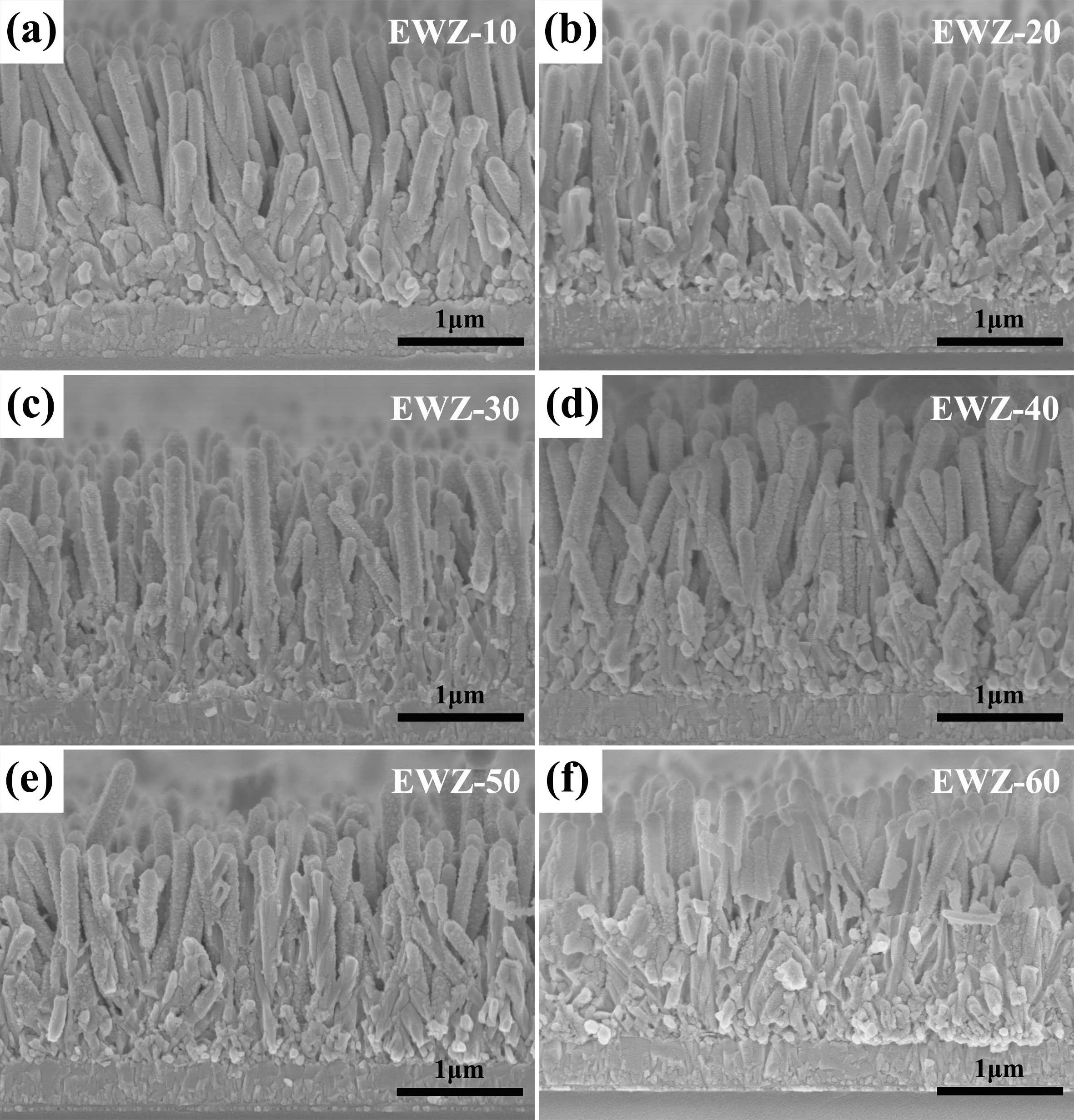
Fig.3. (a)-(f)Cross-sectional SEM images of EWZ array films obtained under different reaction times (10 min, 20 min, 30 min, 40 min, 50 min, and 60 min).
To further explore the effect of simultaneous etching and W-doping on the microstructure, TEM, HRTEM and EDSmapping investigations were performed,as shown in Fig.4.In the TEM image (Fig. 4(a)), it is obvious that EWZ NTs with a rough surface are formed after the simultaneous etching and W-doping treatment,which is consistent with the SEM results.In the HRTEM image(Fig.4(b)),the observed lattice spacing of 0.309 nm can be well indexed to the(100)crystal plane of wurtzite ZnO,but is slightly larger than the original spacing of the(100)crystal plane of wurtzite ZnO.This can be attributed to the influence of W-doping in the form of substitution and interstitial introduction.[40]In detail,the ionic radius(62 pm)of the W6+ion is similar to that(74 pm)of the Zn2+ion,which can thus either substitute for or be interstitially introduced into the ZnO lattice structure.[41]But general substitutional doping cannot induce an obvious lattice expansion, so should be accompanied by interstitial doping. In addition, the EDS mapping of EWZ nanotubes is shown in Fig.4(c): Zn, O,and W elements are observed and are uniformly distributed, helped by the etching and regrowth process.
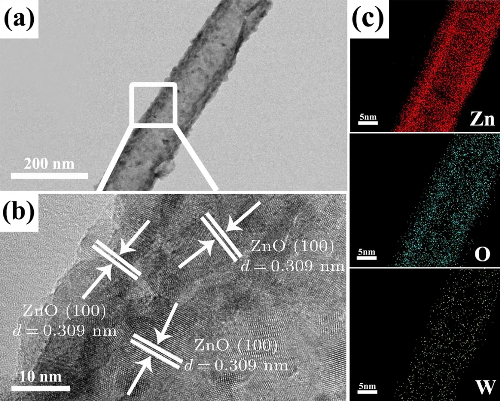
Fig.4. TEM image(a),HETEM image(b)and energy dispersive x-ray spectroscopy elemental mapping(c)of EWZ-40 array films.
The chemical composition and element valence state of EWZ array films were analyzed by XPS spectroscopy, as shown in Fig.5.From the whole XPS spectrum(Fig.5(a))Zn,O,and W elements are observed besides C in air. In detail,for the Zn 2p region (Fig. 5(b)), two standard peaks of Zn 2p3/2and Zn 2p1/2were detected at 1022.2 eV and 1045.2 eV, respectively,which indicates that the valence state of elemental Zn in EWZ array films is+2(Zn2+).[42]For the W 4f region(Fig. 5(c)), two peaks corresponding to W 4f7/2and W 4f5/2are positioned at 35.6 eV and 37.7 eV,respectively,indicating that the corresponding valence state of W in EWZ array films is +6 (W6+).[43]It is worth noting that the valence state of W6+ions is higher than that of Zn2+ions, so more electrons will be introduced by the W-doping process,further resulting in an increase in internal electron density. Therefore,the electrical conductivity of EWZ array films will be significantly increased by W-doping. In addition, the O 1s spectrum can be divided into two peaks centered at 530.4 eV and 531.8 eV after Gauss fitting(Fig.5(d)),which corresponds to the O2-ions of Zn-O and O-H bonds,respectively.[40]

Fig.5. XPS spectra of EWZ-40 array films.
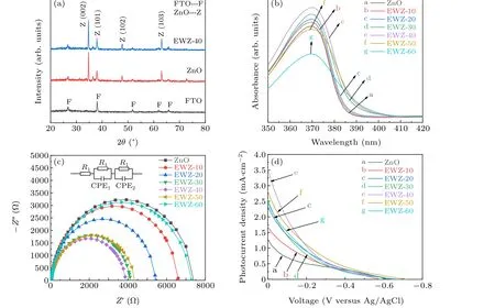
Fig. 6. XRD patterns (a), UV-vis absorption spectra (b), EIS (c) and photocurrent-voltage (J-V) curves (d) of ZnO NR array films and EWZ array films obtained under different reaction times. In the equivalent circuit diagram, R1 and R2 represent the charge transfer resistances of the electrolyte/electrode interface and photoanode/electrolyte interface,respectively. CPE1 and CPE2 represent the capacitors corresponding to R1 and R2,respectively.
Additionally, the effects of simultaneous etching and W-doping on the crystal structure, optical properties, electron transport and PEC performance were further investigated with XRD patterns, UV-vis absorption spectra, EIS andJ-Vcurves, as shown in Fig. 6. In the XRD patterns (Fig. 6(a)),no new diffraction peaks were observed in EWZ array films in contrast to the ZnO NR array films,which implies that the synchronous etching and W-doping treatment does not change the crystal structure of ZnO,consistent with the TEM results.
In the UV-vis spectra (Fig. 6(b)), a typical absorption peak of ZnO is observed at~370 nm owing to its wide band gap (3.37 eV). After the simultaneous etching and W-doping treatment, the absorption edge of EWZ array films shows a slight red shift, which should be attributed to the W-doping that can form proper lattice defects,gap states and intermediate levels to reduce the band gap of ZnO.[40]Furthermore,the light absorption intensity of EWZ array films first enhances and then decreases that of ZnO NR array films with increasing reaction time. This is mainly related to the following factors. Firstly, the rough etched surface can provide more scattering paths to improve the utilization efficiency of incident light.Secondly,the W-doping can reduce the band gap of ZnO and optimize the electron transition mode to improve the lightharvesting ability.[40]However, as the reaction time exceeds 40 min, the blocking of the space between etched nanotubes and the cracking or collapsing of etched nanotubes will result in a significant reduction in light-harvesting ability. Therefore,the light absorption intensity of EWZ array films exhibits the above trend,and the EWZ-40 array films show the highest light absorption intensity.
Similar to the optical properties, the electron transport characteristics of EWZ array films were also effectively improved after the simultaneous etching and W-doping treatment, as shown in Fig. 6(c). In comparison with ZnO NR array films,all EWZ array films display smaller electron transport resistances. As the reaction time is less than 40 min,the electron transport resistance of EWZ array films gradually decreases with increasing reaction time, mainly for the following three reasons. Firstly,the NT structure obtained by etching can provide more direct electron transmission channels than the initial NRs.[40]Secondly, the intermediate levels introduced by W-doping can promote charge transport and separation.[40]Thirdly, the internal electron density of EWZ array films is effectively increased due to the different valence states of W6+and Zn2+ions.[40]However,when the reaction time exceeds 40 min,the etched NTs are cracked or collapsed and the space between etched NTs is blocked;polymerization centers are also formed by excessive W-doping. As a result,the electron transfer resistances of EWZ array films gradually increase due to the reduced surface areas and the increased number of recombination centers. Therefore,the EWZ-40 array films exhibit the smallest electron transport owing to their morphology and W-doping level.
Further investigations of the PEC performance of ZnO NR array films and EWZ array films were conducted with the traditional three-electrode system under simulated sunlight(AM 1.5G 100 mW·cm-2) and theJ-Vcurves are shown in Fig.6(d).It is clear that the photocurrent density of EWZ array films is significantly higher than that of ZnO NR array films,a benefit of the synergistic effect of etching and W-doping.In detail, the etching effect results in a rough surface and the generation of NT structure,which contributes to an improved utilization efficiency of incident light and the quick transportation of electrons. Simultaneously, the uniform W-doping can introduce an intermediate level and more electrons as well as a narrow band gap,thereby improving the light-harvesting ability,promoting charge transportation and separation as well as increasing the internal electron density. Therefore, the photocurrent density of EWZ array films is significantly enhanced.However, the photocurrent density of EWZ array films also tends to decrease as the reaction time exceeds 40 min, consistent with the above optical properties and electron transport characteristics. This behavior is primarily ascribed to the destroyed morphology and the formation of W-doping polymerization centers with the increased reaction time. In conclusion, the optimal reaction time for the simultaneous etching and W-doping treatment is 40 min. The photocurrent density of EWZ-40 array films is 3.5 mA·cm-2,which is~2.8 times higher than that of ZnO NR array films.
3.3. Characteristics of CdS/EWZ composite films
Based on the synchronous etching and W-doping treatment, CdS QDs with a narrow band gap were sensitized on the optimal EWZ-40 array films to further improve PEC performance. Figure 7 shows the cross-sectional SEM images,TEM image,HETEM image and EDS mapping of CdS/EWZ composite films. In the SEM images(Figs.7(a)and 7(b)),it is clear that the CdS QDs densely and uniformly cover the EWZ NRs, giving a rough etched surface that can provide a larger surface area and more active sites for the loading of CdS QDs.The TEM and HRTEM images(Figs.7(c)and 7(d))imply that good heterojunction interfaces are formed between CdS QDs and EWZ,which will be very favorable for the transportation and separation of photogenerated charges. The observed lattice spacings with a value of 0.309 nm and 0.358 nm correspond well to the (100) crystal plane of ZnO and the (100)crystal plane of CdS,[40]respectively. Additionally, the EDS mapping(Fig.7(e))indicates that the elements(Zn, O,W,S,and Cd)comprising CdS/EWZ composite films are evenly distributed.
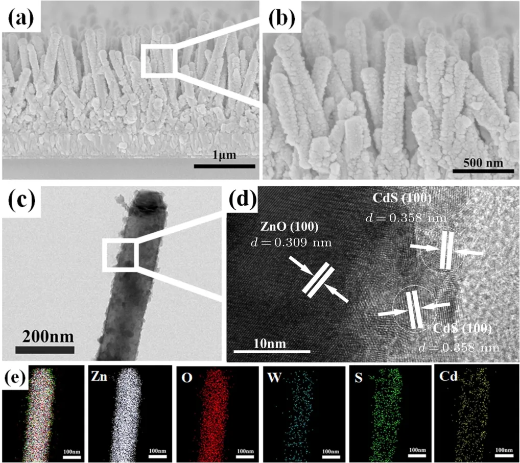
Fig.7. Cross-sectional SEM images[(a),(b)],TEM image(c),HETEM image(d)and EDS mapping(e)of CdS/EWZ composite films.
The XRD patterns, UV-vis absorption spectra,J-Vcurves and EIS spectra of CdS/EWZ composite films are displayed in Fig. 8. From the XRD patterns (Fig. 8(a)), a weak diffraction peak (24.8°) corresponding to the (100) plane of CdS is observed in CdS/EWZ composite films as well as the diffraction peaks of the FTO substrate and EWZ array films,directly proving the existence of CdS QDs. In the UV-vis absorption spectra(Fig.8(b))it is clear that the light absorption edge of the CdS/EWZ composite films displays an obvious red shift and extends to the visible light region, in contrast to the EWZ array films (Fig. 6(b)), due to the introduction of CdS QDs with a narrow band gap.[40]In addition, as the number of SILAR cycles increases, the light absorption edge of the CdS/EWZ composite films appears red-shifted. This is because the size of the QDs will affect the band gap of CdS due to the quantum confinement effect. When the size of the CdS QDs is smaller than the Bohr radius,there will be a strong blue shift phenomenon.[44]This is because the near-continuous energy band will be transformed into discrete energy levels,causing the band gap to widen, and the wide band gap will shift the absorption range to the short wavelength band. However, the gradual increase in the size of CdS QDs will cause the blue shift phenomenon to weaken and disappear.[45]Therefore,as the number of SILAR cycles increases,the size of the CdS QDs also gradually increases,[46]and the light absorption edges of the CdS/EWZ composite films gradually appear to red shift. Simultaneously, the light absorption intensities of CdS/EWZ composite films also display obvious enhancement benefitting from the excellent light-harvesting ability of CdS QDs.
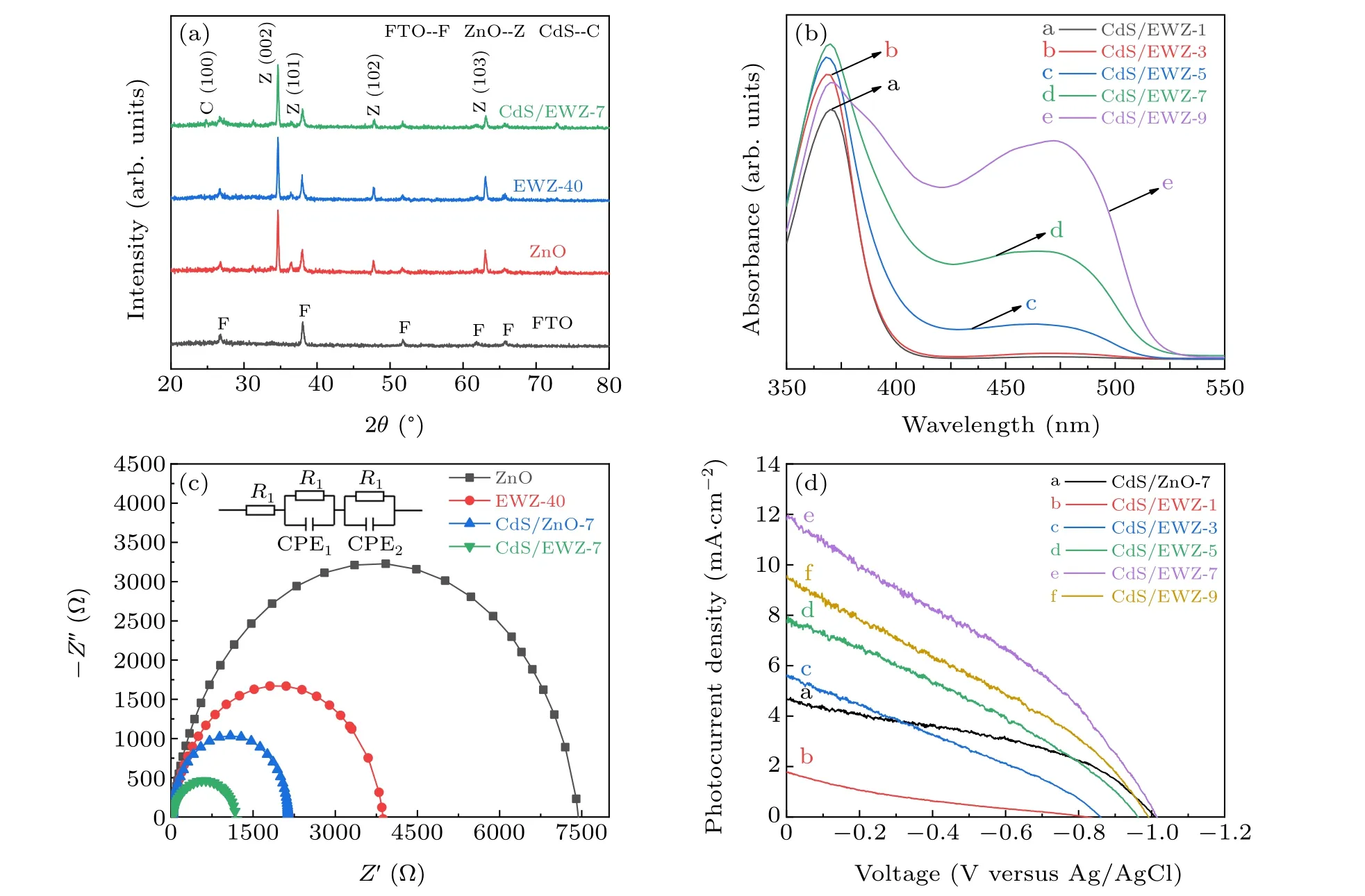
Fig.8. XRD patterns(a),UV-vis absorption spectra(b),EIS(c)and J-V curves(d)of CdS/EWZ composite films with different numbers of SILAR cycles(1,3,5,7,9).
As shown in Fig. 8(c), the charge transfer resistances of CdS/EWZ-7 and CdS/ZnO-7 composite films are better than that of EWZ-40 film. This is because CdS/EWZ and CdS/ZnO heterojunctions are formed after compounding CdS QDs,which is not only conducive to increasing the number of charges but also to improving the separation and transport performance of electron-hole pairs. Furthermore,the CdS/EWZ-7 composite film has better electron transport performance than the CdS/ZnO-7 composite film. This is because the surface area of the EWZ NTs is increased compared with the ZnO NRs. Therefore, the heterojunction area of the CdS/EWZ-7 film is larger than that of the CdS/ZnO-7 film,which is more conducive to the separation and transmission of photogenerated charges.
Based on the better light utilization efficiency and charge transport performance,the CdS/EWZ composite films exhibit remarkably enhanced photocurrent densities compared with the EWZ array films,as shown in Fig.8(d).Moreover,with increase in the number of SILAR cycles,the photocurrent densities and voltages of CdS/EWZ composite films display a firstly increased and then decreased trend. When the number of SILAR cycles is less than 7,the photocurrent density and voltage of the CdS/EWZ composite films increase with increase in the number of SILAR cycles.This is because as the number of cycles increases,the number of CdS QDs gradually increases,thereby increasing the CdS/EWZ heterojunction area and improving the light absorption performance. The CdS/EWZ-7 composite film exhibits the highest photocurrent density and voltage. The maximum photocurrent density at 0 V versus Ag/AgCl is 12 mA·cm-2,which is 3.4 times higher than that of the EWZ-40 array film. The maximum voltage at a photocurrent density of zero is 1.014 V,which is also higher than that of the EWZ-40 array film. The remarkable enhancement of photocurrent density and voltage is mainly related to the high-quality loading of CdS QDs on EWZ-40 array film and the improved light utilization efficiency. In comparison with ZnO NR array films, EWZ array films can provide a larger surface area and more active sites for CdS QDs to effectively increase the loading of CdS QDs. Furthermore, the uniform distribution of CdS QDs and the good interface connect between CdS QDs and EWZ-40 array films (see Figs. 7(c) and 7(d)) can effectively promote the separation of electron-hole pairs and avoid the recontact of electrons with the electrolyte.Therefore,the CdS/EWZ-7 composite films exhibit a 2.5 times higher photocurrent density and 2.2 times lower electron transport resistance than the CdS/ZnO-7 composite films for the same number of SILAR cycles(see Figs.8(c)and 8(d)). However,when the number of SILAR cycles is more than 7,excess CdS QDs will aggregate to form larger particles. The aggregation of CdS QDs not only results in the loss of the quantum constraint effect but can also prevent the effective transportation and separation of photogenerated charges,thereby leading to an obvious reduction in photocurrent density and voltage.
The mechanism of further enhancement of the PEC performance of CdS/EWZ composite films is analyzed in Fig.9.Typically, a heterostructure can be formed between CdS and ZnO owing to the different level positions, and then a builtin electric field is established to provide the driving force for charge transportation and separation. Therefore, the photogenerated electrons in the conduction band (CB) of CdS will transfer to the CB of ZnO,while the photogenerated holes in the valence band(VB)of ZnO will transfer to the VB of CdS,thereby realizing the effective transportation and separation of photogenerated electron-hole pairs. Compared with the common CdS/ZnO composite films,the CdS/EWZ composite films have the following advantages for enhancing PEC performance. Firstly, the etching treatment can introduce larger surface areas and more active sites for high-quality loading of CdS QDs. The increased number of CdS QDs can elevate the utilization efficiency of light, while the uniform distribution and good heterojunction interface can elevate the injection efficiency of photogenerated electrons from CdS to EWZ by preventing the electrons from recontacting the electrolyte. Secondly, the etched NT structure can provide more direct electron transmission channels to promote the quick transportation and separation of photogenerated charges. Thirdly,W-doping can introduce the proper intermediate levels to optimize the electron transmission mode and further promote charge transportation and separation by providing a stronger driving force.Fourthly, the W-doping can introduce more electrons to increase the internal electron density owing to the different valence states of the W6+and Zn2+ions,and thus enhance photocurrent density. Therefore, the CdS/EWZ composite films exhibit a significantly enhanced PEC performance compared with the common CdS/ZnO composite films.
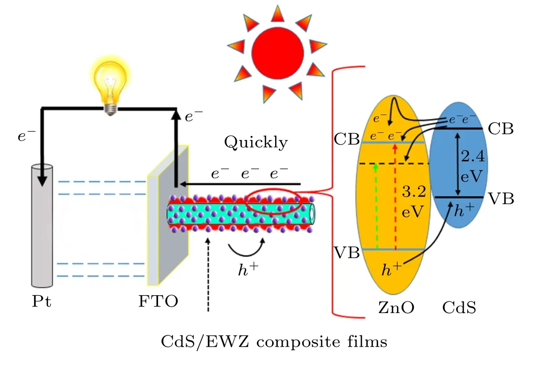
Fig.9. Schematic illustration of band structure and the photogenerated carrier transportation and separation process of CdS/EWZ composite films(CB,conduction band;VB,valence band).
4. Conclusion
In summary,the surface characteristics(surface area,active sites and electronic structure)of ZnO NR array films were synthetically optimized by a self-designed simultaneous etching and W-doping treatment. In contrast to ZnO NR array films, the etched and W-doped ZnO NT array films have a larger surface area, more active sites and better energy band structure for PEC reactions. More importantly,they are more advantageous for the high-quality loading of CdS QDs.Therefore,a high performance was obtained for CdS/EWZ composite films due to the remarkable improvement in their opticalelectrical characteristics. The optimal photocurrent density of CdS/EWZ composite (12 mA·cm-2)is 9.6 times higher than that of ZnO NR array films. This study provides an effective strategy for significantly improving the PEC performance of ZnO-based materials.
Acknowledgments
Project supported by the National Natural Science Foundation of China (Grant Nos. 61904098 and 11904209), the Natural Science Foundation of Shandong Province, China(Grant No. ZR2019QF018), and Higher Education Research and Development Program of Shandong Province, China(Grant No.J18KA242).
猜你喜欢
杂志排行
Chinese Physics B的其它文章
- Erratum to“Accurate determination of film thickness by low-angle x-ray reflection”
- Anionic redox reaction mechanism in Na-ion batteries
- X-ray phase-sensitive microscope imaging with a grating interferometer: Theory and simulation
- Regulation of the intermittent release of giant unilamellar vesicles under osmotic pressure
- Bioinspired tactile perception platform with information encryption function
- Quantum oscillations in a hexagonal boron nitride-supported single crystalline InSb nanosheet
