Characterization of a nano line width reference material based on metrological scanning electron microscope
2022-05-16FangWang王芳YushuShi施玉书WeiLi李伟XiaoDeng邓晓XinbinCheng程鑫彬ShuZhang张树andXixiYu余茜茜
Fang Wang(王芳) Yushu Shi(施玉书) Wei Li(李伟) Xiao Deng(邓晓)Xinbin Cheng(程鑫彬) Shu Zhang(张树) and Xixi Yu(余茜茜)
1National Institute of Metrology,Beijing 100029,China
2Tongji University,Shanghai 200092,China
3Shenzhen Institute Technology Innovation,National Institute of Metrology,Shenzhen 518038,China
Keywords: critical dimension,line width,metrological scanning electron microscopy,traceability
1. Introduction
Accurate measurements of nanostructures (e.g., pitch,height,and width)are crucial to manufacturing at the nanometre scale. Discussions regarding CD have dominated research in recent years due to its importance. As described in the International Technology Roadmap for Semiconductors(ITRS),the measurement uncertainty of the physical CD needs to be reduced to 0.7 nm in the year 2024.[1,2]The CD structure generally consists of top CD(TCD), middle CD(MCD),bottom CD (BCD), circular angle, and sidewall angle, as shown in Fig. 1. Restricted by the level of the manufacturing process,most of the CD structure is trapezoidal. Because of variety of TCD and BCD, we usually define MCD as the feature value of CD.Currently, a multitude of techniques have been developed for the CD measurement,for instance,atomic force microscopy (AFM), transmission electron microscopy (TEM),and scanning electron microscopy (SEM). AFM can generate three-dimensional (3D) images of material surfaces with a high spatial resolution near the atomic scale.[3–5]Its image is a combination of the actual surface topography and the tip geometry used during scanning. Normally, the tip geometry should be estimated first, including the detailed parameters,such as tip diameter, vertical edge height, and tip radius.[6–8]Then one can reconstruct the true specimen shape from the distorted image by the morphological operations of dilation and erosion. However,the accurate estimation of the tip geometry is arduous because the AFM scanning can easily result in tip damage. Daiet al.[9]described the standard deviations limited to approximately±5 nm based on the AFM methods.

Fig.1. Key parameters of a nano line width.
TEM is a distinguished CD measurement method recently, especially after the entry of the Si{220}lattice parameter (d220=192.0155714×10⁻¹²m,uc=0.0000032×10⁻¹²m)into the mise en pratique at the 2018 meeting of the Consultative Committee for Length(CCL).[10]If the CD sample contains monocrystalline silicon,the line features and the periodical silicon crystal lattice planes can be clearly visible in an image with the mode of high-resolution transmission electron microscopy(HRTEM)or scanning transmission electron microscopy (STEM).[11]For the internal CD structure made of monocrystalline silicon, its value is the number of crystal planes multiplied by the lattice constant(see Fig. 2(a)). Otherwise, the CD needs to be calculated by the lattice constant and the pixel span of the crystal planes and the line width(see Fig. 2(b)).[1,12]The TEM method is traced to the metre definition of the International System of Units(SI)via the lattice constant and has superior measurement accuracy. However,its measurement needs the sample milled to a lamella with a thickness of approximately 50 nm by a dual-beam FIB instrument or an ion beam thinner,[12]as illustrated in Fig.3. Consequently,the TEM is a destructive measurement that demonstrates inconvenience in terms of the quantity value transfer.
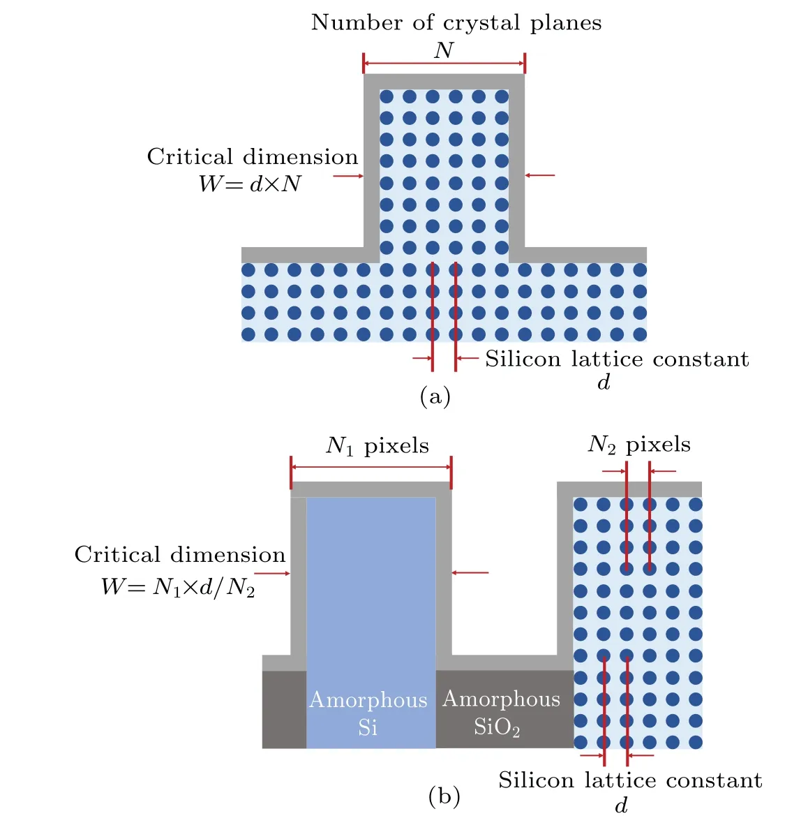
Fig.2. CD measurement principle based on TEM for monocrystalline silicon(a)within the CD structure and(b)outside the CD structure.

Fig.3. Sample preparation of the TEM method.
SEM, based on the secondary electron (SE), is also widely applied to the CD measurement for its high resolution and efficiency.[13–15]Since the SEM method can only obtain the two-dimensional top view of the CD structure,the estimation of the MCD is the distance between the two half intensity points in a line scan.[13]Therefore, an appropriate algorithm is indispensable to extract the widths from the intensity profile after obtaining the SEM images. Currently, the model-based library(MBL)for the CD determination,which was written as an international standard (ISO/DIS 21466.1) in 2019,[16]is a mainstream method. It can be divided into two phases:
MBL generation The MBL is a set of simulated SE linescan profiles,which is produced by the Monte Carlo(MC)simulation with the experimental and specimen geometric parameters. First,one needs to establish an MBL simulator and a specimen model. The MBL simulator consists of the electron probe model described by a gaussian beam model or a focusing beam model, the SE signal generation model, and the SE signal detection model. The specimen model is generated based on the constructive solid geometry(CSG)method[17]or the finite element triangle mesh (FETM) method[18]with the parameters of its material property and geometry,for instance,top CD,middle CD,bottom CD,height, and sidewall angles.Second,the MBL database can be generated based on the MC simulation.[19]Then the process is repeated for the designed inputs parameters to form the library.
CD determination After acquisition of an SEM image,one should find the best fit of the measured image of lines with the simulated SE linescan profiles according to the least square method.[15]Within the range of the library data,the CD values can be obtained.
The results indicate the usefulness of the MBL method for the CD precise extraction from the SEM image. However,for each sample material and CD value, a corresponding library needs to be produced,which is a huge project and inflexible in the actual measurement. As an example,the existing MBL in our laboratory is only suitable for the CD structure manufactured by Au and the CD value greater than 200 nm.
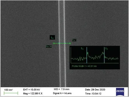
Fig.4. Manual measurement of the line width.
In fact,the actual measurement is manual using the SEM integrated software. That is, the profile is obtained by manually pulling a straight line across the two edges on the image,as the green line L0shown in Fig.4. Then one can manually move the two vertical lines L1and L2on the profile to the half intensity position of the two edges. The value of profile widthl=43.61 nm displayed in the image is the measurement result.However,this manual operation method greatly relies upon the experience of the engineers and would inevitably introduce measurement errors. For instance, is the pulled straight line really straight? How does one know whether the junction of two straight lines (L1, L2) and the two edges is the half intensity position? Furthermore, the more detailed process is a black box to us, which would be not conducive to evaluating the reasonableness of the measurement results.
To solve these problems, this paper presents a more detailed study on the nano line width reference material including its traceability, measurement method and results evaluation based on the metrological SEM.Section 2 introduces the sample,instrument,and measurement algorithm. In section 3,we have evaluated the measurement results in detail from the errors introduced by the sample homogeneity and stability,instrument, algorithm, and repeatability. The limitations of the traceability by the laser wavelength are discussed.Finally,this paper is summarized and concluded in Section 4.
2. Metrological SEM imaging and image processing
2.1. Sample and metrological SEM
The sample TJNIM-160-80-40 prepared at Tongji University was applied in this study (see Fig. 5(a)). The sample has a size of 2.5 mm×2.5 mm×2 mm and consists of three nominal CD values 160 nm,80 nm,and 40 nm.The nanostructure is converted through the thickness of the deposition layer based on the multilayer method.[1]A group of 500 nm SiO2layers,on 160 nm,80 nm and 40 nm Si layers,were deposited on Si(111)wafer surface by radio frequency magnetron sputtering technology. Then the fabrication of the nanostructure is completed by bonding,cutting,grinding,polishing,and selective etching. The thermocompression bonding method is adopted to improve the bonding quality and eliminate the side effect.[20]Figure 5(b)illustrates the layout nanostructure. An SEM image(see Fig.5(c))gives a close view of the line features.
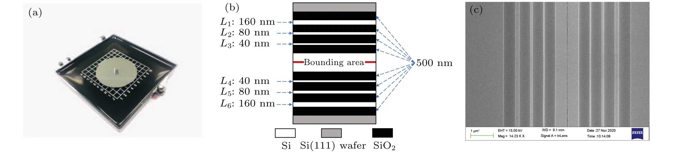
Fig.5. Photos of the CD sample fabricated at Tongji University: (a)photograph of the sample investigated in this study,(b)schematic diagram showing the layout of the nanostructure,(c)an SEM image showing the measured line feature.
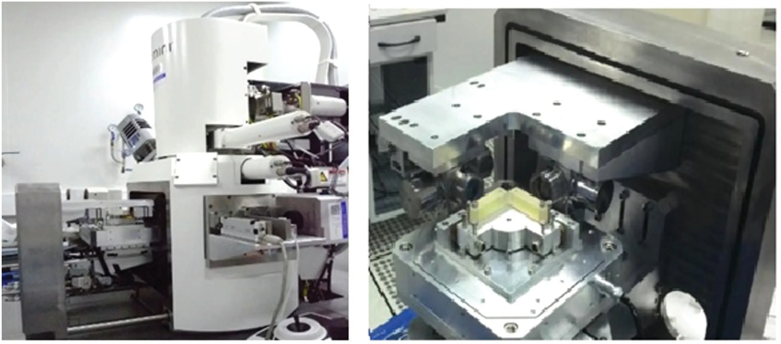
Fig.6. Photo of the metrological SEM developed by NIM in China.
In order to realize the precise measurement of the nanostructures by SEM, National Institute of Metrology (NIM) in China has developed a metrological SEM(see Fig.6). As one of the highest measurement standard devices for nanometrology in China,this instrument has integrated a laser interferometer displacement measurement module. The module is based on the Agilent 10706BV high-stability planar interferometer and uses the L-shaped double-reflecting plane mirror as the measuring mirror,which is fixed together with the sample on the nano-stage. Thex,ypositions of the nanopositioning stage are recorded in real time by VC++ and LabVIEW8.5. Consequently, the image scale of the metrological SEM can be traceable to the SI metre definition.
Hence, samples are all measured by the metrological SEM to ensure the traceability and accuracy of the results in this study.
2.2. Measurement of the nano line width
2.2.1. Top, bottom and middle location
With an e-beam energy of 15 kV and 768 pixels×1024 pixels in the metrological SEM, 160 nm, 80 nm, and 40 nm lines were imaged at the magnification of 110.74×103,125.46×103,and 122.88×10³(see Fig.7),respectively. The averaged intensity profiles of the marked area in Figs. 7(a),7(c), and 7(e)are shown in Figs.7(b), 7(d), and 7(f). For the sake of simplicity,we introduce the averaged intensity profile given in Fig. 7(f) as an example. By zooming in the profile(see Fig.8),one can clearly see two important issues concerning the accurate measurement results.

Fig.7. Measured metrological SEM image and the averaged intensity profile of the marked area: (a)metrological SEM image of 160 nm CD,(b)averaged intensity profile of the marked area in(a),(c)metrological SEM image of 80 nm CD,(d)averaged intensity profile of the marked area in(c),(e)metrological SEM image of 40 nm CD,(f)averaged intensity profile of the marked area in(e).
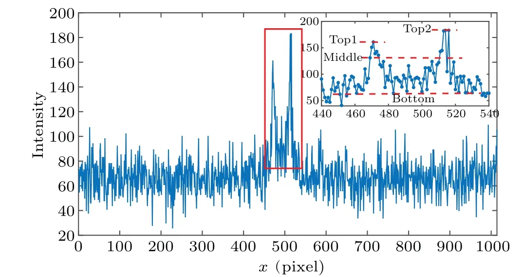
Fig. 8. A zoom-in view of the profile marked in the red rectangular window.
First,there is a significant difference in intensity between the peaks of the left and right edges of the line, leading to questionable top location areas and consequently the top location becomes a major error source. Usually, the background noise is a factor affecting the top location. In our study, the wavelet transform is applied to reject noise. The wavelet basis function is Daubechies 4 wavelet(DB 4)and the decomposition level is 2. In addition,since the sample needs to be fixed on the sample stage by carbon double-sided tape(see Fig.9),the uneven force of the tape on the sample will cause an invisible sample tilt to the naked eyes. Thus, the sample tilt is another factor that may influence the top location. To level the intensity profile,the bottom plane of the profile is linearly fitted. According to the slope of the fitted curve, the incline angleθcan be estimated. Then based on Eq.(1),the profile is rotated clockwise byθaround the point(xc,yc),which can be randomly selected from the matrix.

Second, at the half intensity position, there may not be two corresponding sampling points at the two edges of the line,which can easily lead to large errors in the measurement results. In order to address this issue, we have established a function modely=F(x)of the intensity profile,and solve the variablex=F-1(Ihalf)at the half intensity.
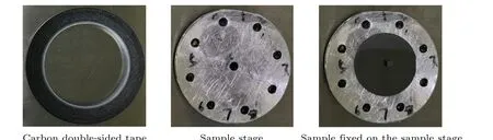
Fig.9. Photos of fixing the sample on the sample stage.
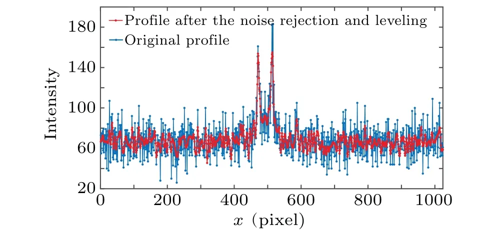
Fig. 10. Comparison of the intensity profile before and after noise rejection and leveling.
According to the features of the line width and the intensity profile, Gaussian and Lorentz functions are utilized for characterization:

whereLscaleis the distance of the scale in the metrological SEM image, Δxis the pixel span of the scale, andKis the scaling factor.

Fig.11. Comparison of the original and model profiles.
2.2.2. Automatic measurement
As described in the introduction, there is a lot of uncertainty in the manual extraction of the CD value from the SEM images. Hence,this paper further studies the automatic implementation of the CD measurement.
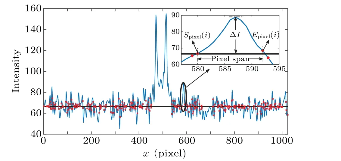
Fig.12. Decomposition of the intensity profile.
The intensity profile can be decomposed into sub-profiles based on the mean-crossing points. Figure 12 is the decomposition of the intensity profile (see Fig. 10), where- is the mean boundary,*is the start and end pixel of the sub-profile,Spixel(i)is the start pixel of theith sub-profile,Epixel(i)is the end pixel of theith sub-profile, ΔIand pixel span are the attributes of the sub-profile. As can be seen, the two edges are included in the same sub-profile. That is due to the fact that their intensity is significantly higher than the background and they can be regarded as anomaly. Hence, we can adopt machine learning methods to identify those anomalies in the intensity profiles. Due to the limitation of sample size, thekmeans algorithm,the most studied and widely used method in unsupervised learning,is applied to anomaly identification.
According to the decomposition of the intensity profile,each sub-profile can be described by the feature vectorpi,

The intensity profile (see Fig. 10) is decomposed into 150 sub-profiles. Each sub-profile has a 1×2 feature vector. Hence,Dis a 150×2 matrix. The initial mean vectorμ1=p1,μ2=p2. The mean vectorsμ1andμ2are not updated in the twelfth iteration. Then the iteration stops. Figure 13 shows the result of cluster division in part of the iteration process. Finally,the cluster division is
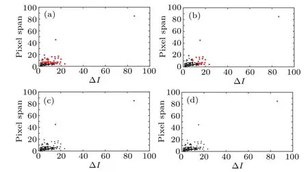
Fig.13.The result of the k-means algorithm(k=2)after each iteration:(a) 1st iteration, (b) 5th iteration, (c) 10th iteration, (d) 11th iteration.Noise sample points and CD sample points are represented by black dots and red dots,respectively.
The sub-profile corresponding top75is given in Fig.14.It shows thatp75is exactly the CD we need to identify. The start pixelSpixel(75)and end pixelEpixel(75)of the sub-profilep75can be easily obtained by indexing because the pixel information of each sub-profile has been stored during profile decomposition.
After accurately identifying the two edges of the CD,the intensity profile is divided into two segments and characterized based on Eq.(3):

Then,Itop,IbottomandIhalfare estimated according to the top,bottom and middle location method.Finally,the CD valueWis calculated by Eq. (5). The process of CD estimation is given in the flow chart(see Fig.15).

Fig.14. The sub-profile corresponding to p75.
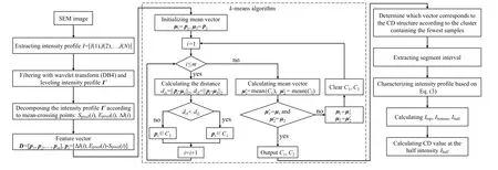
Fig.15. Flow chart of CD estimation.
3. Experimental investigations
Based on the proposed method,researchers A and B have measured the TJNIM-160-80-40 sample six times with the metrological SEM separately, and take the average value as the standard value of the line width,as listed in Table 1. During the experiments, the parameters of the metrological SEM were set to 15 kV e-beam energy and 768 pixels×1024 pixels. For the setup of magnification,it should ensure that there is a complete line width in the field of view. The environmental conditions of the instrument are temperature(20±0.5)°C,and relative humidity≥60%.
3.1. Evaluation of measurement results
Standard deviation is the basic issue in evaluating the measurement results. Measurement errors mainly come from the sample, instrument, algorithm, and repeatability. Their corresponding uncertainty is denoted asu1,u2,u3andu4.Therefore,the combined standard uncertainty is wherec1,c2,c3, andc4are the sensitivity coefficients.According to “Guide to the Expression of Uncertainty in Measurement”,[21]these uncertainties are analyzed as follows.
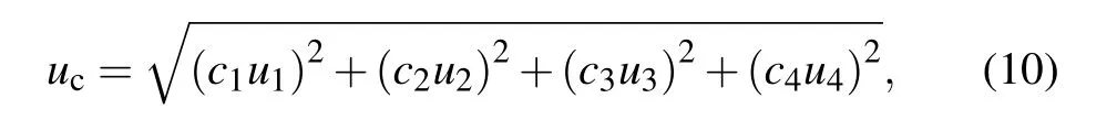
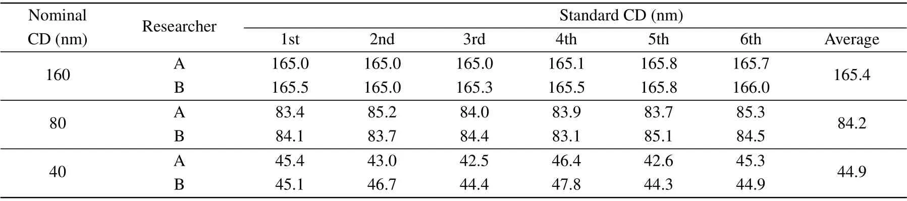
Table 1. Measurement results of the line width sample.
(1) Sample The uncertaintyu1of the sample is mainly composed of homogeneity and stability:
wherem=6 andn=10.The sum of squares of the within-unit is
whereν1=m-1=5 andν2=m(n-1)=54. Therefore,the homogeneity uncertaintiesshfor the 160 nm, 80 nm, and 40 nm CDs are 0.39 nm,0.37 nm,and 0.46 nm,respectively.
Stability is used to describe the time distribution characteristics of the CD value and can be evaluated by the variation of multiple measurements for different time intervals at the same position in the sample. Fitting the obtained data points to a linear functionW=b1t+b0,wheretis the time andWis the CD value,we can get the stability uncertainty

In this study,the time period is one year,respectively,in July 2020, August 2020, September 2020, November 2020,January 2021, March 2021, and June 2021. Hence,t=[0,1,2,4,8,12] andT=12. The stability uncertaintiesstof the 160 nm, 80 nm, and 40 nm CDs are 0.24 nm, 0.60 nm,and 0.60 nm,respectively. Their uncertaintiesu1are 0.46 nm,0.71 nm,and 0.76 nm according to Eq.(11).

Fig.16. Measurement position for homogeneity test.
(2)Instrument The sample to be measured is magnified and imaged by the metrological SEM. The basic unit of the digital image is the pixel,and the actual size represented by a pixel is closely related to the magnification of the microscope and the resolution of the image analysis system.Therefore,the measurement system needs to be calibrated during the measurement process. The uncertainty introduced by the calibration of the instrument is evaluated by the type-B evaluation.The “Certificate for Examination of Measurement Standard”of the metrological SEM shows the relative expanded uncertainty isUrel=3%,k=2. Then the uncertaintyu2is
whereWnis the nominal CD value.Thus the instrument uncertaintiesu2of the 160 nm,80 nm,and 40 nm CDs are 2.40 nm,1.20 nm,and 0.60 nm.
(3) Algorithm In the algorithm, we define the top locationItopas half of the peak intensity of the two edges,as displayed in Eq. (2). The inconsistency of the peak intensity of the left and right edges causes the uncertainty ofItop. The bottom locationIbottomis the mean value of the baseline intensity. The connection between the edge and the baseline is not abrupt, but there is a smooth transition area. The uncertainty of whereIbottomtakes the transition area will affect the measurement result. Therefore, the uncertainty of the algorithm needs to be considered.
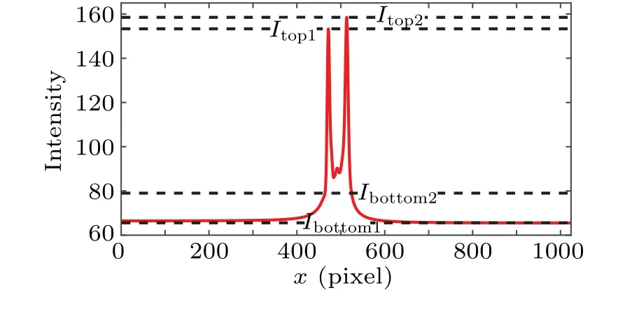
Fig.17. Measurement position for homogeneity test.
Figure 17 is a schematic diagram of the variation range ofItopandIbottom. The maximum relative measurement error
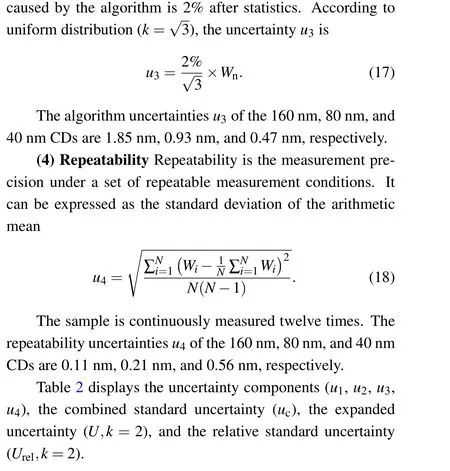
Table 2. Measurement uncertainty evaluation.
3.2. Discussion
The method proposed in this article can meet the measurement requirements of a CD value≥40 nm. However,because the method defined by the laser wavelength traceability to the SI metre definition is limited by interference fringe subdivision and nonlinearity,its measurement uncertainty cannot be further reduced. The traceability method may no longer be applicable with the CD value decreasing.For example,the CD below 32 nm in the integrated circuit requires a measurement uncertainty of less than 10%, in which the proposed method would not guarantee to meet. At present, the TEM method based on the crystal lattice has excellent performance at the atomic scale. However, enough attention needs to be paid to its limitations,such as the destructive measurement and the location of the structure edges which are influenced by the contrast, oxygen layers, and the surface roughness, to improve measurement accuracy. Therefore,the following work will focus on the research of atomic scale nanometrology based on TEM.
4. Conclusion
This paper introduces a nano line width reference material with the 160 nm,80 nm,and 40 nm nominal CD values that are measured by a metrological scanning electron microscope and are traceable to the SI metre definition by the laser wavelength.The proposed method adopts noise rejection,leveling profile,half intensity, model characterization, and other ways to improve the CD measurement accuracy. The automatic identification and measurement of the CD are realized based on the intensity profile decomposition and thek-means algorithm. We experimentally analyze the uncertainty caused by the sample,instrument,algorithm,and repeatability. The relative standard uncertaintiesUrel(k=2)of the 160 nm,80 nm,and 40 nm CDs are 3.9%,4.3%, and 6.5%, respectively. Therefore, the reference material can be applied to calibrating the length value of the scanning electron microscope and other nanometer measurement equipment.
Acknowledgements
This work was supported by the National Key Research and Development Program of China (Grant No.2020YFF0218403)and the Basic Scientific Research Operating Fund of NIM(Grant No.AKYZD2007-1).
猜你喜欢
杂志排行

Chinese Physics B的其它文章
- Erratum to“Boundary layer flow and heat transfer of a Casson fluid past a symmetric porous wedge with surface heat flux”
- Erratum to“Accurate GW0 band gaps and their phonon-induced renormalization in solids”
- A novel method for identifying influential nodes in complex networks based on gravity model
- Voter model on adaptive networks
- A novel car-following model by sharing cooperative information transmission delayed effect under V2X environment and its additional energy consumption
- GeSn(0.524 eV)single-junction thermophotovoltaic cells based on the device transport model