Thermionic electron emission in the 1D edge-to-edge limit
2022-05-16TongyaoZhang张桐耀HanwenWang王汉文XiuxinXia夏秀鑫ChengbingQin秦成兵andXiaoxiLi李小茜
Tongyao Zhang(张桐耀) Hanwen Wang(王汉文) Xiuxin Xia(夏秀鑫)Chengbing Qin(秦成兵) and Xiaoxi Li(李小茜)
1State Key Laboratory of Quantum Optics and Quantum Optics Devices,Institute of Opto-Electronics,Shanxi University,Taiyuan 030006,China
2Collaborative Innovation Center of Extreme Optics,Shanxi University,Taiyuan 030006,China
3Shenyang National Laboratory for Materials Science,Institute of Metal Research,Chinese Academy of Sciences,Shenyang 110016,China
4State Key Laboratory of Quantum Optics and Quantum Optics Devices,Institute of Laser Spectroscopy,S
hanxi University,Taiyuan 030006,China
Keywords: vacuum microelectronics,thermionic emission,graphene,electronic transport in nanoscale materials and structures
1. Introduction
Due to the power-hungry nature and difficulty for circuit integration, vacuum tubes had to give their way to solid-state electronic transistors even though they were glowing and popular for several decades in the modern history of electronics.In a vacuum tube, a thermionic emission current can be collected between the electrically isolated anode and the heatedcathode when a voltage is applied in the anode electrode.Compared with traditional silicon devices,vacuum tubes have several compensating beneficial effects despite their defects.[1]For example,the maximum transmission rate of an electron in a vacuum tube is very high, and they have excellent durability upon radiation bombardments. Up to now, vacuum tubes have been demonstrated in various applications,such as x-ray tubes,[2,3]vacuum sensors,[4,5]and display.[6,7]
To date, thanks to the state-of-the-art nano fabrication technology,vacuum tubes with nanoscale can be successfully fabricated, which opens the door of a new research field,i.e., vacuum nanoelectronics.[8–10]Early attempts to fabricate miniaturized vacuum tubes mainly used on the diamond,silicon, molybdenum, and other multilayered Si-based thin films as emitters, which showed considerably high emission currents.[11–15]However,they often suffer from fragility of dielectric breakdown, and stringent requirements of high vacuum.
Beyond these traditional materials, graphene and other two-dimensional(2D)materials have attracted a great deal of attention for their excellent properties, such as high electrical and thermal conductivities, good chemical stability, high melting point.[16,17]Furthermore,several works have demonstrated that 2D materials, such as graphene and MoS2, are capable to serve as resistive channels carrying large electrical current densities,[18–21]making them suitable candidates for nanoscaled filaments in thermionic electron emitters. Recently,different configurations of vacuum tubes using graphene as the electron emitter were studied,[22–25]high ONOFF ratio,[23]fast temporal response, and controllable electron emission[24]were obtained. A monolayer WSe2vertical field emission transistor has also been fabricated,[26]the emission current exhibited good stability with a W-tip hung up at a distance of a few hundreds of micrometers. However,a stand-alone vacuum tube device fully made of van der Waals(vdW) heterostructures, especially down to the 1D edge-toedge emission limit,has not been studied.
Here, we report a 1D edge-to-edge thermionic emission vacuum tube with nano-sized vacuum gaps(~200 nm)using graphene with/without hexagonal boron nitride(h-BN)encapsulation. One-dimensional edge-to-edge thermionic emission is realized when the emitter graphene is Joule-heated by exerting a current density of about 1 mA/μm in it. The acceptor current from vacuum tunneling exhibits a rectifying behavior,which pushes the thermionic emission to the single atomic 1D limit. The maximum emission current in our 1D edge-to-edge configuration can reach 200 pA. We also find that the maximum emission current is increased with the layers of graphene.
2. Results and discussion
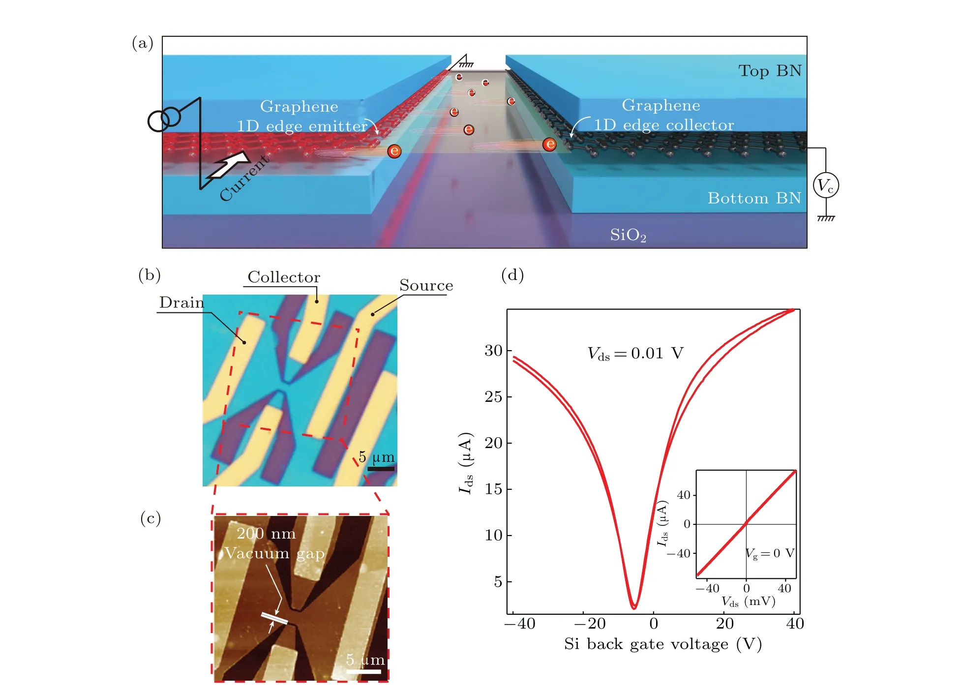
We first demonstrate an architecture of a vacuum tube in the 1D single-atom-edge limit with graphene sandwiched by h-BN,as depicted in the illustration in Fig.1(a). When the encapsulated graphene is Joule heated as a hot filament,electrons are escaping from the 1D edge under a collector tension due to much lowered work function, and shoot through the vacuum gap onto the 1D collector,thus forming an edge-to-edge thermionic emission transistor. As seen in the optical image of a typical device in Fig.1(b),by introducing a 200 nm vacuum gap in the h-BN/monolayered-graphene/h-BN sandwich,the emitter and the collector are electrically isolated,with the nano gap defining the 1D edge-to-edge vacuum channel, as seen the atomic force microscopy (AFM) image in Fig. 1(c).Meanwhile,1×1 μm2of the area of hot filament was designed in order to rapid heating. Before the test of thermal emission,we first characterize the basic electrical transport properties of the device at room temperature. A typical bipolar transport with an obvious Dirac point was obtained from the transfer curve, i.e., the source-drain currentIdsdependent on the Si back gate in the range of±40 V, as shown in Fig. 1(d). Inset image of Fig.1(d)shows theI–Vcurve with Si back gateVg=0 V, source-drain voltageVds=±50 mV, a near-linear ohmic characteristic was observed.
For typical devices,monolayer graphene starts to act like a bright bulb when the current density is about 1.2 mA/μm,with thermionic emission taking place at a source–drain voltageVdslarger than 15 V. As shown in Fig. 2(a), the typical emission current versus collector voltage(Iemission–Vcollector)of monolayer graphene with h-BN encapsulation at differentVdsis illustrated in aVcollectorrange of±40 V.It can be seen that theIemissionbecomes measurable at a source-drain voltageVdslarger than 15 V and the curve ofIemission–Vcollectorshows a diode rectifying behavior above this emission threshold. The emission current increases with the source–drain voltage,i.e.,current density in the graphene emitter,and a maximum emission current of 6.5 pA was obtained before graphene broke down atVds=18.3 V due to extreme thermal and/or electrical stress. Interestingly, a small loop occurs in theIemission–Vcollectorcurve in the small-bias regime. This phenomenon is also seen in non-encapsulated monolayer graphene emitters,as will be discussed in the coming Fig.3(a). We attribute it to a possible electro-chemical reaction of such as water molecules captured at the edge of graphene edges,further investigations on this matter however need to be carried out.
To better understand the thermionic emission taking place in this system, we measured the black body radiation (BBR)spectra for variousVds. As shown in Fig. 2(b), the intensity of emission spectra monotonically increases asVdsincreases, and the central wavelengths of the spectra are distributed around~760 nm. In our optical system,the quantum yield of CCD (DCCD(λ)), the reflection efficiency of optics coating (DRef(λ)), and the diffraction efficiency of the grating(DGra(λ))were considered during our estimation,thus the total detection efficiency of our optical system,D(λ), can be expressed asD(λ)=DCCD(λ)×DRef(λ)×DGra(λ). Thus,the calibrated BBR can be expressed asI′(λ)=I(λ)/D(λ),whose central wavelength can be determined precisely. After that, we estimate the radiation temperature of graphene with an h-BN encapsulated emitter by comparing the central wavelength ofI′(λ)with that of the Planck radiation formulaλ-3[ehc/λkT-1]-1,whereλis the frequency of thermal radiation,cis the speed of light in vacuum,Tis the temperature,handkare Planck’s constant and Boltzmann’s constant,respectively. As shown in Fig. 2(b), BBR spectra were well fitted,and a levitation of temperature from about 2580 K to 2880 K,withVdsranging from 10 V to 16 V, was obtained. A similar result has been reported in Ref. [18], such high temperature also agrees with a mechanism of field-assisted thermionic emission.
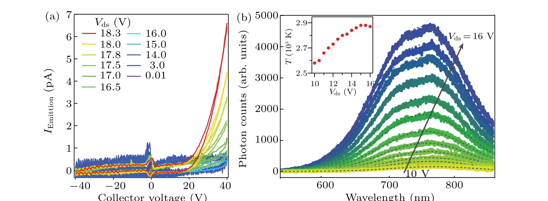
Fig. 2. Thermionic emission characteristics of 1D edge-to-edge emitter with h-BN encapsulated graphene. (a) Iemission–Vcollector curves in a Vcollector range of±40 V.Traces and retraces are recorded. (b)Black body radiation spectra as a function of radiation wavelength at different Vds. Black dashed lines are fitted curves. Inset: temperatures dependent on source–drain voltage Vds estimated from(b).
In the following, we study the graphene without h-BN encapsulated vacuum tubes using the same framework as the h-BN encapsulated graphene above. Firstly, a vacuum tube based on monolayer graphene was fabricated, as seen in Fig. 3(a). The characteristic of thermionic electron emission is basically the same as h-BN encapsulated graphene. Typical rectifying behavior can be observed in theIemission–Vcollectorcurves as well,and the maximum emission current was about 8 pA at 40 V collector voltage. The small hysteresis loop below the emission threshold also appears,in agreement with the samples encapsulated by h-BN.In order to improve the maximum emission current,we increased the number of layers of graphene.Figure 3(b)illustrates the thermionic emission characteristics of the vacuum tube based on 15 layers of graphene without h-BN encapsulation. The maximum emission current was raised to 130 pA and the ON-OFF ratio was reaching 103(shown in the inset in Fig.3(b)).
For comparison, we fabricated multiple in-plane graphene (with different layers) nano-vacuum-gapped emitter devices without h-BN encapsulation, and similar rectifying behaviors are found in them. Clearly, with the increasing number of layers, the thermionic electron emission current is enhanced up to 200 pA (for 40 layers of graphene),along with the enhancement of the power and breakdown current of the emitters, as shown in Figs. 3(c)–3(e). The enhancement of maximum emission current with the increasing thickness of graphene can be well explained by the simplified Richardson–Dushman model,[27]which is expressed asIemission=AT2e-w/kT. In our 1D edge-to-edge graphene vacuum tubes,the work functionWis constant.Assuming that the temperature of the emitter would be the same in the thermionic emission regime, theIemissionwill be proportional to the constantA,which has a positive relationship with the surface area of the emitter,in qualitative agreement with the experimental observations.
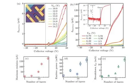
Fig.3. Thermionic emission characteristics of 1D edge-to-edge emitters without h-BN encapsulated graphene. (a)Iemission–Vcollector curves in a Vcollector range of±40 V of monolayer graphene vacuum tube. Traces and retraces are recorded. Inset: Optical image of the device,red dashed region and black dashed region are emitter and collector of the vacuum tube, respectively. (b)Iemission–Vcollector curves in a Vcollector range of±40 V of 15 layers graphene vacuum tube. Traces and retraces are recorded. Inset:same data in(b)is plotted in a log scale at Vds=6.69 V.For the scenario of non-encapsulated graphene emitter,the number of graphene layer dependences are plotted for(c)maximum emission current(before the breakdown of emitter channel), (d) power, and (e) breakdown current of the emitter channel, respectively. Data was obtained at 300 K in a vacuum chamber of about 10-2 mbar.
3. Conclusions
To summarize, we have successfully fabricated a nanoscale vacuum tube in the 1D edge-to-edge limit using graphene with/without h-BN encapsulated as a thermionic emitter. The as-prepared devices exhibit thermionic emission current up to 200 pA,with a characteristic rectifying behavior.An ON-OFF ratio of 103is achieved in the edge-to-edge emission. Optical spectroscopy analyses suggest the black body temperature of about 2580–2880 K in the emitter. Our results push the thermionic emission to the single atomic 1D limit using the vdW assemblies as a platform,and may pave a way for future nano-electronic systems based on it.
4. Method
In this work,graphene(monolayer and multilayer)as well as encapsulating h-BN flakes were directly mechanically exfoliated onto a SiO2/Si substrate from the high-quality single crystal. A Bruker Dimension Icon AFM was used for thicknesses and morphology tests. The BN-encapsulated graphene stacks were fabricated under ambient conditions, using the dry-transfer method.[28]The final stack on the SiO2/Si substrate was annealed in a chemical vapor deposition furnace in argon and hydrogen atmosphere (40:4) at 320°C for 30 min to completely remove the residual polymer. Metal electrodes(Ti/Au=5/50 nm)were fabricated by standard electron beam lithography using a Zeiss Sigma 300 SEM with a Raith Elphy Quantum graphic writer and electron beam evaporation. After lift-off, graphical processing should be performed to isolate the emitter and collector using the reactive ion etching. The high precision of current measurements of the devices was measured using a LakeShore vacuum probe station at room temperature and about 10-2mbar, with an Agilent B1500A semiconductor device parameter analyzer. The spectroscopy of black body radiation was detected at room temperature under ambient conditions using a spectrometer (Andor, Shamrock, SR-303i) and a cooled charge-coupled device (CCD,iVac 316), while the DC voltage was applied by a Keithley 2400. The detection efficiency of the optical system as a function of wavelength was calibrated before testing.
Acknowledgements
This work was supported by the National Natural Science Foundation of China (Grant Nos. 12004389, 12004288,and 12104462) and the China Postdoctoral Science Foundation (Grant Nos. 2020M68036 and 2021T140430). Xiaoxi Li acknowledges the support from the Joint Research Fund of Liaoning-Shenyang National Laboratory for Materials Science (Grant No. 2019JH3/30100031). Hanwen Wang acknowledges the support from the IMR Innovation Fund(Grant No.2021-PY17).
杂志排行

Chinese Physics B的其它文章
- Erratum to“Boundary layer flow and heat transfer of a Casson fluid past a symmetric porous wedge with surface heat flux”
- Erratum to“Accurate GW0 band gaps and their phonon-induced renormalization in solids”
- A novel method for identifying influential nodes in complex networks based on gravity model
- Voter model on adaptive networks
- A novel car-following model by sharing cooperative information transmission delayed effect under V2X environment and its additional energy consumption
- GeSn(0.524 eV)single-junction thermophotovoltaic cells based on the device transport model