Photon number resolvability of multi-pixel superconducting nanowire single photon detectors using a single flux quantum circuit
2022-05-16HouRongZhou周后荣KunJieCheng程昆杰JieRen任洁LiXingYou尤立星LiLiangYing应利良XiaoYanYang杨晓燕HaoLi李浩andZhenWang王镇
Hou-Rong Zhou(周后荣) Kun-Jie Cheng(程昆杰) Jie Ren(任洁) Li-Xing You(尤立星)Li-Liang Ying(应利良) Xiao-Yan Yang(杨晓燕) Hao Li(李浩) and Zhen Wang(王镇)
1State Key Laboratory of Functional Material for Informatics,Shanghai Institute of Microsystem and Information Technology,Chinese Academy of Sciences,Shanghai 200050,China
2Center of Materials Science and Optoelectronics Engineering,University of Chinese Academy of Sciences,Beijing 100049,China
3CAS Center for Excellence in Superconducting Electronics,Shanghai 200050,China
Keywords: superconducting nanowire,single-flux quantum circuit,photon number resolution
1. Introduction
Superconducting nanowire singlephoton detectors(SNSPDs) have exhibited superior performance over other singlephoton detectors(SPDs)in terms of high detection efficiency,low dark count rate,low time jitter,and wide response band. They have been widely used in quantum information processing,[1,2]deep-space laser communication,[3]satellite laser ranging,[4,5]mid-infrared emission spectrometry,[6]and other applications. In SNSPDs, a detection event is triggered by the hotspotinduced biascurrent redistribution in the readout circuit, and the pulse amplitude of SNSPDs is typically determined by the bias current and the subsequent amplifiers, regardless of the number of photons. As a result, it is generally believed that intrinsic photon number resolvability(PNR) in SNSPDs is absent, although some efforts on PNR in SNSPDs have been reported.[7]However, SPDs with photon number resolvability are essential for several applications,such as linear photon quantum computation and near-infrared spectroscopy.[8,9]Aiming at implementing PNR in SNSPDs,multi-pixel SNSPDs or SNSPD arrays have been proposed to resolve the number of incident photons.[10,11]Recording the detection signal of anN×NSNSPD array requires at least 2Nbias-tees and amplifiers.[12]Furthermore, the large number of operating hot cables in a large SNSPD array requires a compact and efficient cooling system.
To minimize the thermal power introduced by the readout circuit,a single-flux quantum(SFQ)circuit has been proposed. This circuit has demonstrated its ability to convert and register the signals obtained from SNSPD arrays into SFQ digital pulses. In 2009, Teraiet al.first used SFQ circuits to convert the signals obtained from SNSPD arrays into SFQ pulses by employing an interface circuit named as “magneticfield coupled DC-to-SFQ (MC-DC/SFQ) converter”.[13–15]Later, SFQ read-out circuits based on the MC-DC/SFQ converter were further developed to determine the origin of the detection pulse from SNSPD arrays.[16–19]Moreover,such SFQ read-out circuits can be integrated on the same chip as the SNSPD array, which further improves the integration level at low temperatures and makes practical applications feasible.
To determine the number of detected photons, the SFQ read-out circuits need to either resolve the amplitude of detection pulses or directly record each pixel. Myorenet al.employed a multi-stage MC-DC/SFQ module with six different response thresholds to achieve a six-photon resolution.[16]This method requires careful design of the coupling response threshold current of each MC-DC/SFQ converter coil, and the number of DC/SFQ modules increases linearly with the number of resolved photons. Myorenet al.also used multiple MC-DC/SFQ to directly connect each pixel in an SNSPD array.[20]Using the output terminal of a multi-level doubleflux-quantum amplifier connected in series with the MCDC/SFQ module,the response signals from the SNSPD arrays can be converted into the output voltage amplitude, which is proportional to the number of response pixels. This design requires an extremely large chip area,which is costly for counting a dozen of photons.
In this work, a method employing a multi-input magneticfield coupled DC-to-SFQ converter (MMD2Q) circuit is proposed as a read-out circuit in multi-pixel SNSPD devices.This MMD2Q circuit provides PNR through signal combining and amplitude discrimination. The successful operation of an SNSPD array integrated with the MMD2Q converter circuit in a compacted Gifford–McMahon (GM) cryocooler is also demonstrated. The results confirm that the MMD2Q circuit can be applied to achieve PNR in multi-pixel SNSPDs.
2. Circuit simulation and measurement
Compared with conventional MC-DC/SFQ circuits, the proposed MMD2Q circuit can be used for signal combination and amplitude resolution in multi-input SNSPD arrays and provides a simple way of recording signals obtained from SNSPD arrays with PNR.In this section,the MMD2Q circuit is initially designed. Subsequently, its operation is simulated and tested. Finally, an SNSPD array device coupled with the MMD2Q circuit is installed in a compact GM cryocooler,and PNR is verified.
2.1. Circuit design
The circuit design is based on the cell library of the SIMIT Nb/Al-AlOx/Nb SFQ process. The critical current intensity of the Josephson junctions is 6 kA/cm2.[21]Figure 1 presents a schematic diagram of the designed MMD2Q,which consists ofn50 Ω resistors connected in parallel, a transformer, 2 Josephson junctions, a Josephson transmission line(JTL), and an SFQ/DC converter (Q2D). Each SNSPD is in series with a 50 Ω on-chip resistor, and the SNSPDs are in parallel with each other, which are connected in series withL1.L1combines each signal from the SNSPD pixels and couples the combined signal to the transformer coil. To avoid the SNSPD signal crosstalk caused by different pixels, the transformer impedance is intentionally designed to be small compared with the impedance of the SNSPD pixels. The transformer consists of two coils (L0andL1) and two junctions(J0andJ1). TheL0andL1inductances are 13.6 pH and 1.8 nH,respectively,and they are coupled by a mutual inductanceM=105 pH.The junctionsJ0andJ1transform the input SNSPD pulses into SFQ pulses,in which the critical current is 92.5 μA. The transformer bias current (I0) inJ0,J1, andL1adjusts the threshold input amplitude currentIth. Owing to the highly integrated MMD2Q circuit, the chip size is approximately 5 mm×5 mm, which is significantly smaller than the half-wavelength of the SNSPD GHz-frequency signal. Therefore, the MMD2Q circuit can be simplified to a lumped circuit model. The signal transmission path lengths of the pixels are almost equal (length difference<1 cm). Therefore,the time difference among the superimposed signals of each pixel is limited below the SNSPD geometric jitter time level(typically~12 ps for an NbN SNSPD with an active area of 10×10 μm).[22]The amplitude of the superimposed signals atL1has a linear relationship with the number of detected photons.
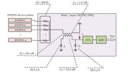
Fig.1. Schematic diagram of the MMD2Q circuit.
Regarding the MMD2Q circuit operation,the SNSPD signal is initially coupled and amplified by the transformer,which in turn triggersJ0, and an SFQ pulse is, therefore, generated.The number of SFQ pulses generated can be expressed as follows:

whereΦ0is a single magnetic flux quantum,Icis the critical current ofJ0andJ1,Il1is the current flow inL1,Ithis the threshold current ofL1that generates one SFQ pulse inJ0,andI0is the bias current ofJ0. Then,the SFQ pulse is transmitted to the output converter (SFQ/DC: Q2D) through the JTL. Finally, the Q2D converts the output SFQ pulse into an edge-jump signal, i.e., the signals from the detected photons are transformed into a series of edge-jump signals.
2.2. Simulation of the MMD2Q circuit
To validate the performance of the designed MMD2Q circuit, an open-source PSCAN2[23]simulator was used to simulate the transmission and conversion of the input signals before fabricating the circuit. In the simulation, one channel is adopted for the signal input. By tuning the input current amplitude,Ithis obtained when the SFQ pulse appears atJ. The current amplitude resolution ΔI=Φ0/M, which is the amplitude difference of the input current between two converted pulses, determines the lowest current value of the SNSPD’s output signal. In the simulation,ΔIis 19.55 μA.In Fig.2(a),the simulated SNSPD input signal amplitudes are shown in black, and the converted SFQ pulses are shown in red. Four triangular signals with rising and falling edges of 1 ns and different amplitudes were input. Since the MMD2Q circuit could only convert the rising edge of input signals,their falling edges were ignored. For a practical SNSPD pulse,the falling edge is typically an exponential decay with a time constant ofLk/Rl,whereRlis the external load of the read-out circuit(typically 50 Ω). In the MMD2Q circuit, as the input signal amplitude increases,J0is triggered multiple times,proportionally to the input signal amplitude. For example, by inputting signal amplitudes of 37.5/75/150/750 μA to the 50 Ω load resistor,2/4/8/40 SFQ pulses,respectively,are eventually generated by the MMD2Q circuit,as illustrated in Fig.2(a). Figure 2(b)illustrates the simulatedIthof the input signal as a function of the bias currentI0ofJ0andJ1. It can be observed that asI0increases in the Josephson junction,Iththat needs be biased on the SNSPDs decreases. The difference in theIthvalues for different slew rate input signals may result in errors regarding the resulting number of photons.
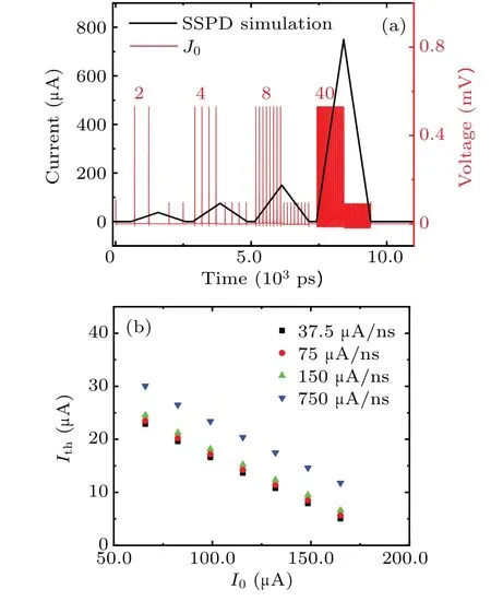
Fig. 2. (a) Simulated input signals with different amplitudes and the corresponding signals converted by the SFQ circuit.The number of the SFQ pulses is marked upon the pulses. (b) Simulated current threshold Ith for different amplitude input signals as a function of the bias current in the transformer module.
2.3. MMD2Q circuit fabrication and testing
The SIMIT Nb/Al-AlOx/Nb SFQ process was employed to fabricate the MMD2Q circuit.[24]For simplicity, four parallel input channels were selected for demonstration. These channels can combine up to four SNSPD signals and then send the combined signal to the transformer. The layout of the fabricated chip is illustrated in Fig.3.
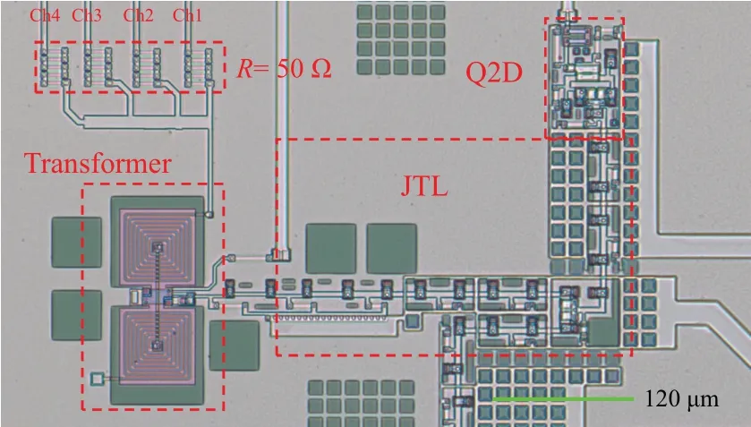
Fig.3.Layout of the fabricated MMD2Q circuit,including four parallel input channels.
The circuit function was verified by first testing the chip using simulated SNSPD signals as inputs. A signal generator(Keysight M8190A)was employed to generate SNSPD signals with different amplitudes. Seven SNSPD analog waveforms with amplitudes ranging from-9.7 mV to-87 mV and a 30 ns pulse width were generated and then sent to the MMD2Q circuit. Owing to the limited amplifier bandwidth, the rising edge of the positive signal was too narrow to be recorded.Therefore, negative signals were employed, which turned a slow recovery edge into a rising edge for recording. The SFQ circuit was mounted on a GM-cryocooler system with a double μ-metal shielding at a 2.5 K base temperature. The ambient magnetic field was measured to be less than 150 nT.The generated signals were attenuated by 24 dB at 2.5 K before being sent to the SFQ circuit(top black waveforms in Fig.4(a)).The output signal from the Q2D module was amplified by the AM-1431 amplifier (bandwidth: 1 kHz to 1 GHz; gain: 40 dB)at room temperature and then registered by the oscilloscope.The red waveforms in the bottom of Fig. 4(a) are the output waveforms of the flipped edges forI0=55 μA. The number of flipped edges denotes the number of photons. Pulse amplitudes of 2.20/2.88/3.43/4.12/4.67/5.35 mV were transformed into a Q2D output signal with 1/2/2/3/3/4 flipped edges, respectively. Owing to the limited amplifier bandwidth,the four flipped edges were not clearly registered in the measurement.Figure 4(b) shows the input signal current amplitude versus the output edge-flip count. An edge-flip count corresponding to 0–4 photons was distinguished from the pulse amplitudes.
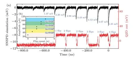
Fig.4. (a)Input-pulse signals and the corresponding output waveforms with flipped edges for a 55 μA bias current. (b)Input signal amplitude versus output edge-flip count. The same color block of amplitude range outputs the same flip count.
2.4. SFQ circuit integrated with SNSPDs
The PNR of the SNSPDs with the MMD2Q circuit was experimentally demonstrated by fabricating a four-pixel SNSPD array withIc= 28 μA. Fabrication details can be found in a previous report.[25]The SNSPD array and the MMD2Q circuit were mounted on the same level with the compact GM cryocooler at 2.5 K(see Fig.5(a)). A schematic diagram of the system is shown in Fig.5(b). Since one of the MMD2Q circuit input channels is reserved for the function verification, three pixels were connected to the MMD2Q circuit using a 15-cm-long semi-flexible coaxial cable. Voltage sources connected in series with 100 kΩ resistors were applied to each SNSPD pixel.
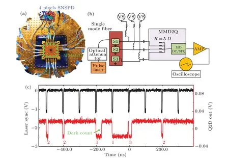
Fig. 5. (a) Layout of the SNSPD array and SFQ circuit installed in the cryocooler. (b) Schematic diagram of the SNSPD array with the MMD2Q converter circuit. (c)Laser input sync signals(black line)with a 10 MHz frequency and corresponding output flipped signals(red line). All three pixels were biased at-25 μA.
To reduce the arrival time difference of different SNSPD signals,the cable length difference for different channels was within a maximum value of 1 cm,corresponding to a less than 50-ps time delay. The input 532 nm laser pulses were generated by PDL 800-B with a pulse half-height width of 55 ps.Three SNSPD pixels were individually biased at-25 μA.To reduce the MMD2QIth,Iwas set to 100 μA, which resulted inIth=22 μA.The laser input sync pulses(black line)with a 10 MHz frequency and a-66 dBm optical power are shown in Fig.5(c). The corresponding output flipped signals with 0, 1, 2, and 3 flips at most can be observed (see the red curve in Fig. 5(c)). The number of flips denotes the number of the SNSPD pixels triggered by the incoming photons,thus demonstrating the PNR of the SNSPD array with the MMD2Q circuit. Note that the gaps between two flips for one inputpulse response in Figs.4(a)and 5(c)are different and related to the decay time, pulse-waveform amplitude, and flip-count threshold.
3. Discussion and conclusion
The PNR of the MMD2Q circuit mainly depends on the maximum sampling ratefand the sampling accuracy ΔIof the circuit. The maximum sampling rate in the proposed circuit,which is determined by the SFQ circuit process parameters,is approximately 50 GHz, and ΔI=Φ/M. For anIinput amplitude signal, the number of photons that can be resolved is equal toI/ΔI.For an SNSPD response pulse with a rising edge of approximately timet1, the maximum PNR of the circuit is equal tot1×f.For example,fort1=1 ns,the theoretical maximum PNR is 50. However,the actual PNR can be reduced by the inconsistency of the SNSPDs and the current redistribution in different SNSPD pixels when one SNSPD is triggered.[12]
Another practical issue affecting the PNR is the amplifier bandwidth in the proposed circuit,which limits the Q2D flipping ability. This problem can be overcome by using a pulse counter based on the SFQ circuit, which directly transforms the combined signals into binary data.
In summary, an MMD2Q circuit employed as a readout circuit in multi-pixel SNSPD arrays, which can implement PNR, is proposed in this work. A four-input MMD2Q circuit and a four-pixel SNSPD array have been fabricated, and a PNR of 3 is successfully demonstrated using three channels.Consequently, this method is effective in implementing PNR in SNSPD arrays.
Acknowledgements
This work was supported by the SELF process platform of the Center for Excellence in Superconductivity Electronics,Chinese Academy of Sciences,and the circuit design and test support provided by the SFQ circuit research group. Thanks to Yongliang Wang, Lingyun Li, Xingyu Zhang and Xiaofu Zhang for fruitful discussions and manuscript preparation.
This work was also supported by the National Key R&D Program of China(Grant No.2017YFA0304000), the Strategic Priority Research Program of Chinese Academy of Sciences(Grant No.XDA18000000),and the Science and Technology Commission of Shanghai Municipality, China (Grant No.18511110200).
猜你喜欢
杂志排行
Chinese Physics B的其它文章
- Erratum to“Boundary layer flow and heat transfer of a Casson fluid past a symmetric porous wedge with surface heat flux”
- Erratum to“Accurate GW0 band gaps and their phonon-induced renormalization in solids”
- A novel method for identifying influential nodes in complex networks based on gravity model
- Voter model on adaptive networks
- A novel car-following model by sharing cooperative information transmission delayed effect under V2X environment and its additional energy consumption
- GeSn(0.524 eV)single-junction thermophotovoltaic cells based on the device transport model
