Study on electrostatic discharge (ESD)characteristics of ultra-thin dielectric film
2022-05-05RonggangWANG王荣刚YurongSUN孙玉荣LiuliangHE贺柳良andJitingOUYANG欧阳吉庭
Ronggang WANG(王荣刚),Yurong SUN(孙玉荣),Liuliang HE(贺柳良) and Jiting OUYANG (欧阳吉庭)
1 Suzhou TA&A Ultra Clean Technology Co.Ltd., Suzhou 215121, People’s Republic of China
2 Beijing Institute of Technology, Beijing 100081, People’s Republic of China
3 College of Science, Beijing University of Civil Engineering and Architecture, Beijing 102616, People’s Republic of China
Abstract Electrostatic discharge (ESD)event usually destroys the electrical properties of dielectric films,resulting in product failure.In this work,the breakdown characteristic of machine mode(MM)ESD on three different nano size films of head gimble assemble are obtained experimentally.The breakdown voltage and thickness parameters show a positive proportional relationship,but they are generally very low and have large discrete characteristics (~30%).The maximum and minimum breakdown voltages of the tested samples are 1.08 V and 0.46 V, which are far lower than the requirement of the current standard(25 V).In addition,the judgment criterion of product damage is given, and the relationship between discharge voltage polarity, initial resistance and breakdown voltage is studied.Finally,the theoretical analysis of the breakdown characteristic law has been given.
Keywords: ultra-thin dielectric film, electrostatic discharge (ESD), machine model
1.Introduction
In the past few decades, there has been a great amount of interest in the breakdown phenomena in micro-scale and the scholars have made a lot of explorations.Micro gap discharge is the breakdown discharge of gas or dielectric film under the micron and nano gap.The study of micro gap discharge comes from the conventional macro-scale gas breakdown discharge.At first, the research on the discharge law of macro-scale(greater than mm)dielectric system was the main research direction.Its electrical breakdown characteristics and discharge law were widely discussed and studied,and a relatively mature theory was formed.Generally, the breakdown voltage of air gap generally meets the classical Paschen’s law [1].
In the 1950s,W Boyle and L H Germer found that when the air gap decreased to a certain critical value,Paschen’s law was no longer applicable, and the micro gap breakdown characteristics began to attract the attention of researchers[2,3].The researchers completed the experimental study on air and vacuum breakdown characteristics in the range of 0.25-100 μm, and studied the influence mechanism and discharge law of different air pressure, different electrode materials and different electrode shapes (needle electrode, ball electrode,cylindrical electrode,flat electrode,etc).J M Torres et al also noticed the differences of micro discharge in the experiment, so conducted a series of studies on the discharge breakdown voltage of the gap below 10 μm [4, 5].After that,the importance of micro discharge-related problems was gradually recognized, and a large number of related basic and applied researches were carried out.P G Slade and E D Taylor had a good discussion on the breakdown of 0.2-40 μm micro gap space discharge, it is pointed out that the breakdown law under the condition of micro gap does not meet the classical breakdown theory under the condition of the uniform electric field, and its mechanism may be more similar to vacuum discharge [6].T Ono et al studied the breakdown characteristics of a micro gap electrostatic actuator.Its electrode is placed on the silicon surface.It is found that the electrode material, gap and dielectric surface state have a great impact on the breakdown voltage.Micro discharge may occur even when it is lower than the average breakdown limit field strength and speculated that this may be caused by the influence of electron emission on the surface of the metal electrode[7].Radmilovic-radjenovic carried out a large number of experiments and simulations.The results showed that field emission cannot be ignored in micro discharge, and the breakdown voltage seriously deviated from the Paschen relationship curve[8,9].J T Ouyang’s team,come from BIT,also studied the needle plate structure and found the relevant laws and mechanisms of discharge curve under micro gap[10,11].
With the further improvement of device integration,experimental research on the structure of nano gap and the breakdown characteristics of devices has been carried out gradually.On one hand, scholars, including Y Hirata, N S Rajput, Y Cheng and V Ziemann, have built nano scale dielectric systems and conducted relatively in-depth research on breakdown law and mechanism.On the other hand, the electronic industry practitioners represented by hard disk heads and integrated circuits have also conducted in-depth research on the DC breakdown characteristics and ESD model breakdown characteristics of various products at the nano scale, confirming the breakdown characteristics of ultra-thin dielectric films.The main research scholars include A Wallash of Maituo company and Z Y Teng of TDK company[12-14].They found that the breakdown mechanism of semiconductor devices with nano gap scale is dominated by field emission, and the breakdown voltage has a great correlation with electrode surface roughness and defects.Although so many research results have been obtained, the breakdown characteristics and mechanism of ultra-thin dielectric films with thickness of 1 nm and below in MM ESD are still not well known.
In this work, we investigate the discharge characteristics in electrode-dielectric film-electrode geometry at 1 nm or less scale.The aim is to understand the breakdown features of the MM ESD breakdown voltage of different test samples and try to obtain the breakdown threshold.
2.Samples and test method
The damage of head gimble assemble (HGA)products is mainly characterized by the change of internal magnetic tunnel junction resistance [15-17].The magnetic tunnel junction is a sandwich structure that is composed of a very thin dielectric film sandwiched between two ferromagnetic sheets.Its structural diagram is shown in figure 1.The dielectric film in the middle is made of AlOx.The size characterization of this dielectric film has three parameters:thickness(MRT),depth(MRH)and width(MRW).When the material is fixed,the test resistance area(TRA)product value can be used to characterize the insulation layer thickness parameter, and unit is Ω·μm2.The insulation layer thickness(MRT)of the samples of three specifications are about 2.2 nm,1.3 nm and 0.9 nm,and the corresponding TRA value is 2.2,1.28 and 0.86 Ω·μm2,respectively.The insulation layer depth (MRH)is about 78 nm, 60 nm and 40 nm.
ESD events can cause soft or hard damage of the device during the assembly processes.Due to the variety of manufacturing processes and application of devices, there are models such as charged human body model (HBM), charged device model (CDM)and the machine model (MM)to evaluate the damage influence of ESD events [18, 19].HBM is used to simulate the discharge of the human body to electrostatic sensitive devices after charging.CDM is used to describe the discharge of ESD-sensitive devices to grounding conductors after charging.Machine model (MM)is used to simulate the ESD events of charged conductors on the machine.The circuit schematic diagram of the machine model is shown in figure 2.
In general, MM has been commonly used to evaluate ESD sensitivity of MR heads at the slider and the HGA level because the waveform is well-defined and easy to generate.When testing,the ESD discharge voltage is usually applied to the two reader pins (R+ and R-).This tester model is QST2002-PLUS Universal Quasi-Static tester.The bias voltage setting is 0.1 V and the scanning magnetic field intensity is+/-300 Oe.The voltage applied to samples starts from 0.3 V and increases in the step of 0.02 V/time until the sample breaks down.The voltage and resistance parameters before and after discharge can be directly recorded by the tester.Twenty samples were tested for each specification.
3.Results and discussion
3.1.Judgment benchmark of breakdown voltage
With the gradual increase of the applied voltage between the positive and negative electrodes, the ultra-thin dielectric film is gradually damaged,which is reflected in the change of MR resistance(MRR)directly.In order to find a suitable judgment benchmark for breakdown, we observed the applied voltage that caused MRR change rate over 5%, 10% and 50%, as shown in figures 3-5, respectively.
It can be seen that with the increase of applied voltage,the samples with a change rate over 5% increase gradually.The voltage of samples is discrete, and the voltage is relatively low.The minimum voltage of samples with TRA = 1.28 Ω·μm2is only 0.46 V, which is lower than that of samples with TRA = 0.86 Ω·μm2(0.52 V).In addition,the voltage points of samples with different parameters are crossed.For samples with TRA = 2.2 Ω·μm2, the voltage causing resistance change is significantly higher than the other two specifications.
Compared with the result with MRR change rate over 5%, the samples with TRA = 1.28 Ω·μm2and TRA = 0.86 Ω·μm2still have the cross point, but they are gradually separated.The applied voltage of the sample with TRA = 2.2 Ω·μm2is still relatively high.
When MRR change rate is over 50%, the voltages with the different dielectric films are further separated,and they are not crossed.Therefore, it is reasonable to define the applied voltage with MRR change rate over 50% as the ‘breakdown voltage’.
3.2.Influence of the thickness of film
When the discharge voltage is applied to the electrodes on both sides,the ultra-thin dielectric film is broken down along the thickness direction.As mentioned above, TRA is usually used to characterize the thickness parameters.In this section,statistics are made on the breakdown voltage of 20 samples of three specifications with an initial resistance change of more than 50%.Figure 6 shows the maximum, minimum and average breakdown voltage of samples of different specifications for comparative observation.
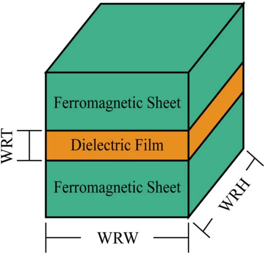
Figure 1.Structure of magnetic tunnel junction.
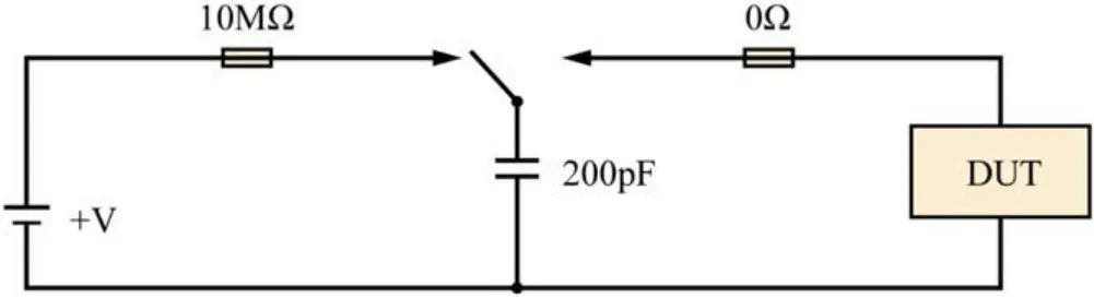
Figure 2.Schematic diagram of MM ESD.
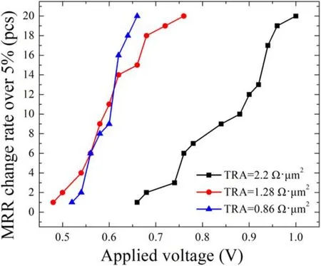
Figure 3.MRR change rate with applied voltage (≥5%).
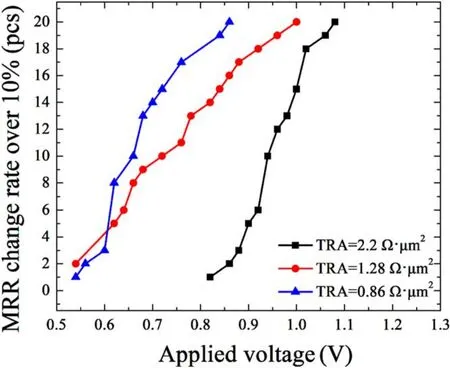
Figure 4.MRR change rate with applied voltage (≥10%).
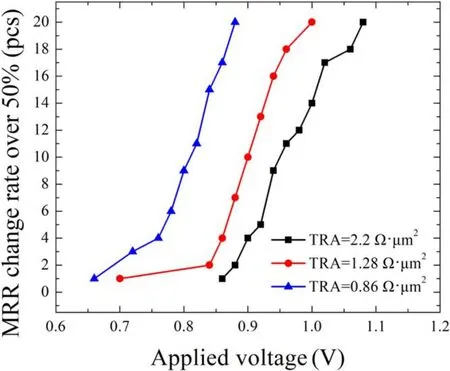
Figure 5.MRR change rate with applied voltage (≥50%).
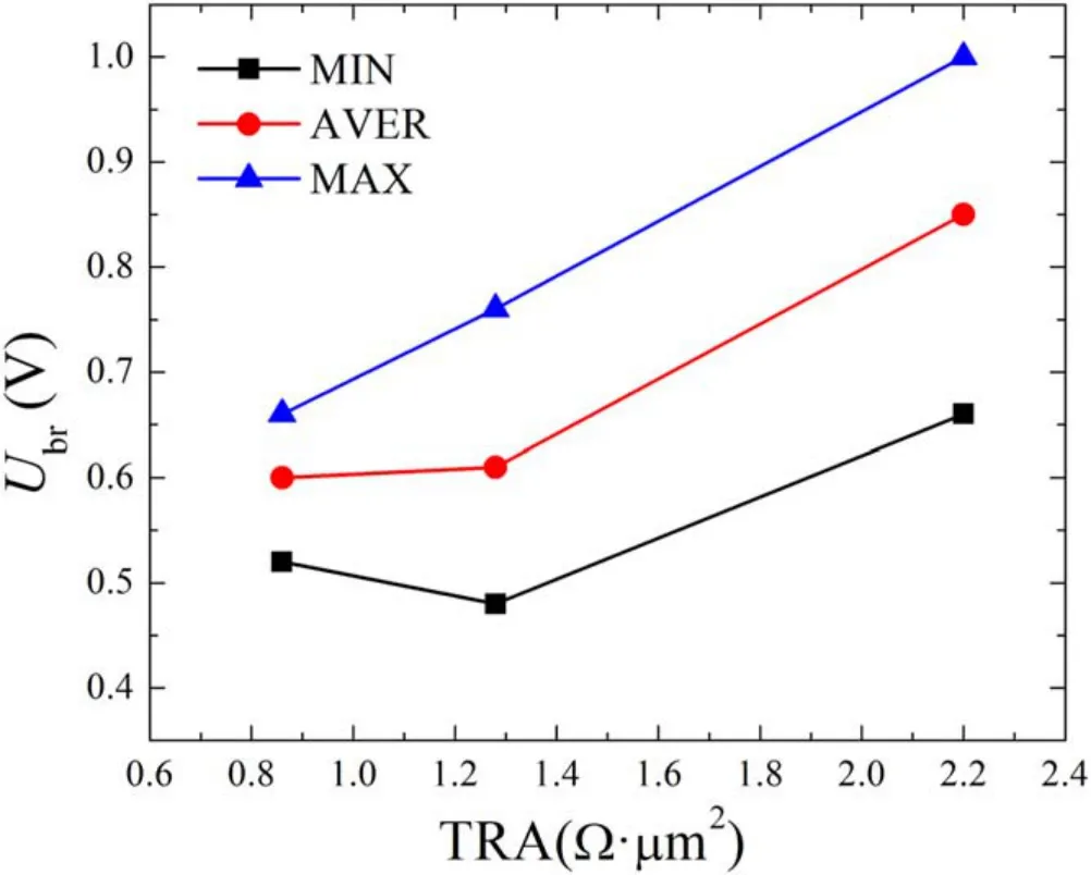
Figure 6.Breakdown voltage of samples varies with the TRA.
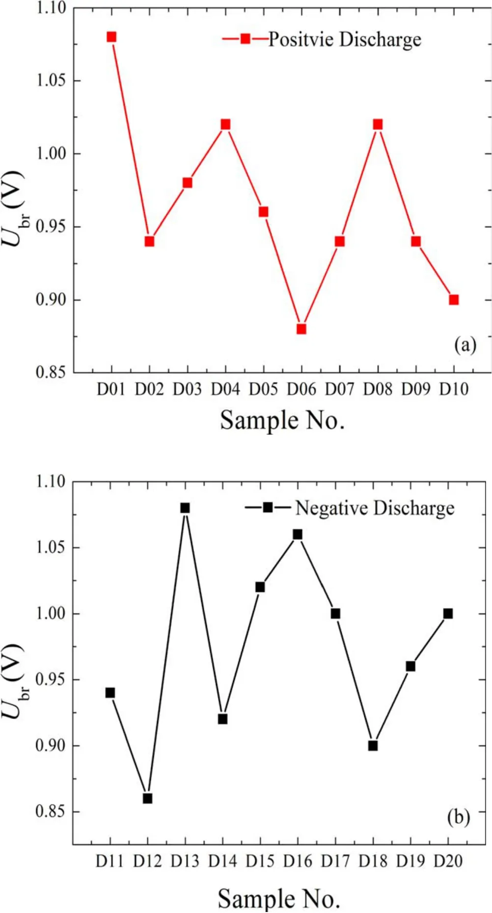
Figure 7.Breakdown voltage distribution of samples with different polarity MM ESD.(a)Positive discharge, (b)negative discharge.
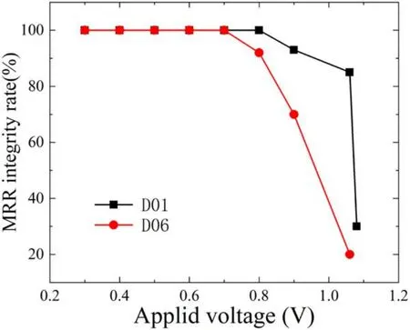
Figure 8.MRR integrity rate with applied voltage.
It can be seen that the breakdown voltage decreases with the insulation film thickness (TRA parameter decreases),whether it is the maximum value, minimum value or average value.Specifically, when TRA = 2.2 Ω·μm2, the maximum,average and minimum breakdown voltages are 1.08 V,0.97 V and 0.86 V respectively.When TRA = 0.86 Ω·μm2, the corresponding three voltages are 0.88 V, 0.66 V and 0.81 V respectively, and the breakdown voltage decreases by nearly 20%, indicating that the breakdown voltage will further decrease with the continuous decrease of dielectric film thickness.
Comparing the breakdown voltages of different samples of the same specification, it can be found that the breakdown voltages have great discreteness.Taking the sample with TRA = 1.28 Ω·μm2as an example, the difference between the maximum and minimum breakdown voltage is 0.3 V,and the dispersion rate is close to 34%compared with the average value of 0.9 V.Such a large discrete characteristic cannot be simply explained by the uneven thickness of the dielectric film.This may be caused by defects in the film.
Further, it can be found that the maximum breakdown voltage is only 1.08 V and the minimum voltage is 0.66 V.The protection requirements of such products will be very strict.
3.3.Influence of discharge polarity and initial resistance
In this part, we divided the samples of each dielectric thickness into two groups and tested the forward discharge and reverse discharge respectively.Taking the sample with TRA = 2.2 Ω·μm2as an example, figure 7 shows the status of breakdown voltage.
It can be seen that the breakdown voltage of MM ESD is distributed between 0.86 V and 1.08 V, and there is no sharp difference between positive and negative.The discrete characteristics of breakdown voltage in the two cases are basically the same.Furthermore, we compare the relationship between breakdown voltage and initial resistance.Table 1 shows the initial resistance of the sample.
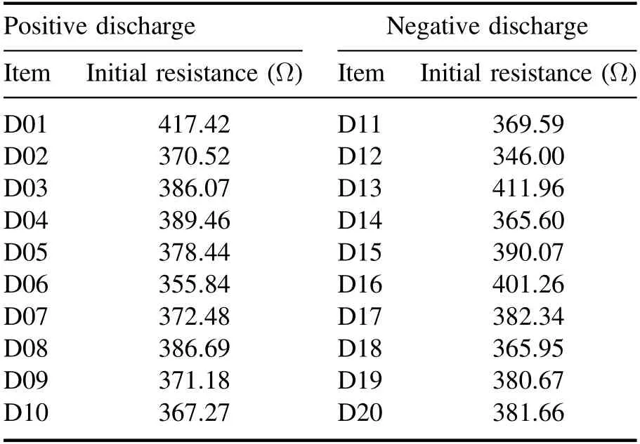
Table 1.Initial resistance of HGA samples.
Compared with the breakdown voltage of each sample,it can be found that the higher the initial resistance is, the greater the breakdown voltage is.Specifically,the breakdown voltages of D01 and D13 are the largest,reaching 1.08 V,and their initial resistances are the largest, 417.42 Ω and 411.96 Ω,respectively.The breakdown voltages of D06 and D12 are relatively small, 0.88 V and 0.86 V, respectively.Correspondingly,the initial resistances are relatively small, 355.84 Ω and 346 Ω respectively.This is because the thicker the ultra-thin dielectric film, the greater the initial resistance and the greater the breakdown voltage.
3.4.Variation law of resistance with applied voltage
In order to better understand the gradual damage caused by the applied voltage to the sample, take two samples D01 and D06 in the specification of TRA = 2.2 Ω·μm2for observation, as shown in figure 8.
It can be seen that once mild damage (soft damage)occurs to the sample, serious damage (hard damage)will occur very quickly.Specifically, when the applied voltage of D06 sample was 0.78 V, its initial resistance decreased by 8%.Then,when 1.08 V,its resistance decreased to 20%, and the sample was broken down and damaged.The performance of D01 is more obvious.When the applied voltage is 0.9 V,its resistance decreases by 7%.When 1.06 V, the resistance decreased by about 15%, and finally, it was completely broken down at 1.08 V.Once the ultra-thin dielectric film is damaged, it will form defects, and the resistance of defect location shows a downward trend.According to the mode parameters of MM ESD, if the breakdown voltage is converted into breakdown energy, samples D06 and D01 are 116.64 pJ,but the energy causing soft damage is 60.84 pJ and 81 pJ respectively.At this time, the resistance is the parallel resistance of the defect location resistance (R1)and other surface area resistance (R2), which is mainly affected by R1.In the subsequent testing, the defect location has low resistance and large passing current,resulting in local heating,and finally expands the area of the defect location, resulting in overall breakdown and damage.This can also well explain the large dispersion of breakdown voltage in the same specification sample.
4.Breakdown mechanism
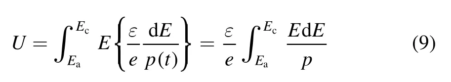
Under the action of the applied electric field, electrons are injected into the dielectric film.With the injection of electrons, the density of trapped holes increases with time [20].The variation law with time can be expressed as:
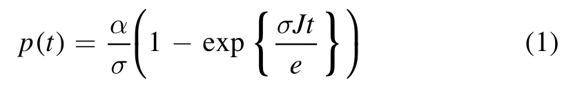
J is the current density, e is the electronic quantity, α is the number of trapped holes generated by collision ionization, σ is the composite number of trapped holes on the composite section.The latter two terms are general functions of the electric field.
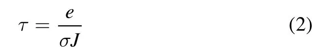
According to the above formula, the maximum hole density can be close to α/σ, which is an equilibrium value.With the development of time, the number of holes increases continuously to reach this equilibrium value.At this time,the resulting holes are balanced by recombination.The time to reach this equilibrium value is:
If the saturation equilibrium level of holes is equal to or greater than the charge breakdown density of the medium,breakdown will occur.
Assume that the capture cross-section is a constant, α depending on the value of the electric field E:

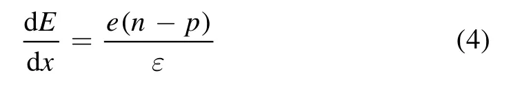
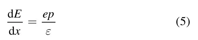
Where H is the avalanche height, which is equal to the exponent of the product of ionization rate and electrode spacing.According to Gauss law, in the one-dimensional case, the derivative of the electric field is equal to the charge in the dielectric film divided by the dielectric constant.
Considering that the hole density in the film is significantly higher than the electron density, the above formula can be simplified as:
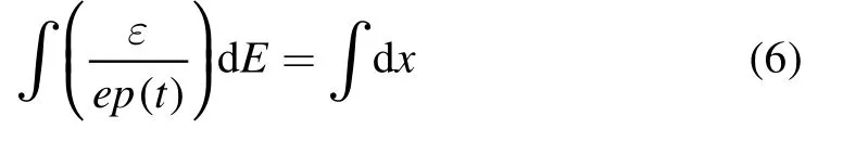
Separating variables, Gauss law is transformed into:
Combined with the expression of Gauss law and hole density, the above formula can integrate along the thickness direction (Tox)of the dielectric film.In order to complete the integration, the electric field and the spatial term need to be separated.We can obtain:
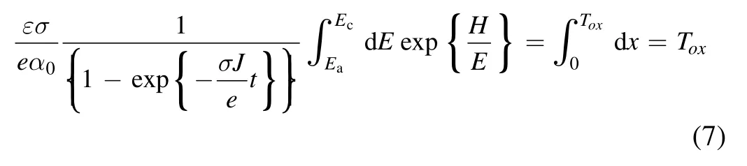
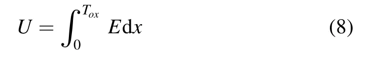
Where,the integral formula is carried out in the film area,and the integral of the electric field boundary is from the positive electrode (Ea)to the negative electrode (Ec).Therefore, the applied voltage on the film can be expressed as the integral of the electric field in this area, that is:
Substituting Gauss law, we can get:
The dimensionless variables defining time,field strength,thickness and voltage are:
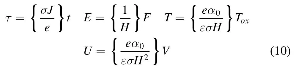
Thus, the voltage of the film can be expressed in a dimensionless formula, that is:
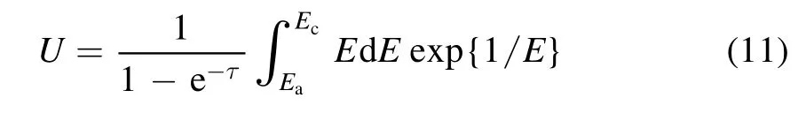
The hole number in the initial film is zero, and the voltage on the film increases with time.If the hole equilibrium value is lower than the breakdown value,the amount of charge in the film will be close to the equilibrium value.When the dielectric breakdown value is exceeded,breakdown occurs.For holes,the breakdown charge can be expressed as:
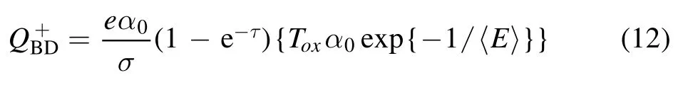
The first part is related to the equilibrium value and the time to reach the equilibrium value.It is not the breakdown condition, but the relationship between ionization and recombination.The latter part is related to ionization and spatial position, which is equivalent to the derivation of breakdown, thus:
The above deformation finishing can be expressed as:
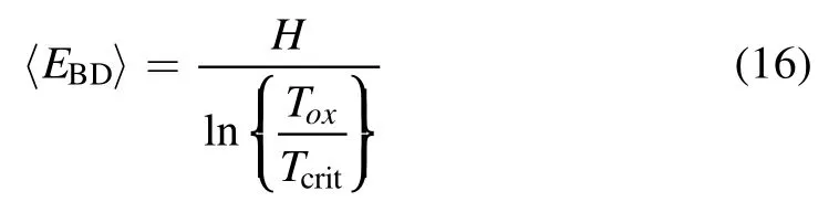
For constant breakdown charge and breakdown time,the above formula can be expressed as the breakdown condition of the average breakdown electric field, i.e.
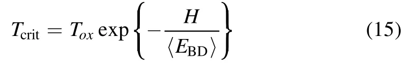
The average breakdown field strength can be calculated as:
In case:
The relationship is:
It can be seen that the breakdown voltage is closely related to the thickness, which is in line with the previous research law, and the breakdown is in line with the field emission-dominated breakdown mechanism.It is the theoretical analysis of the experimental chapter.Further,according to the theoretical formula, the theoretical values are different from the actual experimental values, but they are all in one order of magnitude.This difference is mainly caused by defects and imbalance in the actual samples.In addition, the significance of this theory is to guide researchers to select dielectric materials and estimate theoretical dimensions in design.
5.Conclusions
With the decrease of film thickness, the value of breakdown voltage shows a downward trend, that is, the breakdown voltage is positively correlated with dielectric film thickness and has no relationship with the discharge direction.Whether it is a forward breakdown or reverse breakdown, the ESD breakdown voltage of the film is very low and has great dispersion.The maximum electrostatic breakdown voltage of samples is only 1.08 V, and the minimum voltage is only 0.66 V.The minimum voltage causing soft damage is lower than 0.5 V, which is far lower than the standard requirement of M1 < 25 V.Excellent control measures are required to avoid device damage.In addition,special attention should be paid to the defect points of the dielectric film.The discrete characteristic of breakdown voltage is mainly related to the defects of the dielectric film.
ORCID iDs
杂志排行
Plasma Science and Technology的其它文章
- Numerical analysis on the effect of process parameters on deposition geometry in wire arc additive manufacturing
- Investigation of the gas bubble dynamics induced by an electric arc in insulation oil
- The influence of charge characteristics of suspension droplets on the ion flow field in different temperatures and humidity
- Characteristic studies on positive and negative streamers of double-sided pulsed surface dielectric barrier discharge
- Hydrophobicity changes of polluted silicone rubber introduced by spatial and dose distribution of plasma jet
- Characteristics of water volatilization and oxides generation by using positive and negative corona