2D arsenenes
2022-03-24YiHuJunchuanLiangLixiuZhangZhongJinandLimingDing
Yi Hu, Junchuan Liang, Lixiu Zhang, Zhong Jin,†, and Liming Ding,†
1Key Laboratory of Mesoscopic Chemistry (MOE), School of Chemistry and Chemical Engineering, Nanjing University, Nanjing 210023, China
2Shenzhen Research Institute of Nanjing University, Shenzhen 518063, China
3Center for Excellence in Nanoscience (CAS), Key Laboratory of Nanosystem and Hierarchical Fabrication (CAS), National Center for
Nanoscience and Technology, Beijing 100190, China
Graphene has raised a huge wave in 2D materials field,breeding lots of graphene analogs with applications in optical and electrical devices, energy conversion and storage, biology, etc.[1,2]. Graphene presents superior carrier mobility,while its zero-bandgap restricts its transistor application. To make up this shortcoming, new 2D materials with certain bandgaps and high carrier mobility are being developed.Two typical materials are transition metal dichalcogenides(TMDs) and black phosphorus, which exhibit layered structure, layer-dependent band structure and strong quantum constraints[3−5]. As a congener of phosphorus, arsenic can complement the bandgap of existed 2D materials[6−18]. Arsenic has several allotropes, i.e. semimetal gray arsenic, semiconductive black arsenic and insulating yellow arsenic. 2D arsenic, i.e.arsenenes, were developed.
In 2015, arsenene came into sights after a number of reports on theoretical predictions[6−8]. Monolayer arsenenes with buckled and puckered honeycomb structures were fabricated, and corresponding phonon spectra and electrical band structures were calculated based on density functional theory (DFT) (Fig. 1(a) and 1(b))[6,7]. Both puckered and buckled arsenenes are dynamically stable with an indirect bandgap(Fig. 1(a) and 1(b))[6,7]. Zenget al. calculated the band structures of monolayer, bilayer and trilayer arsenenes, revealing metal-to-semiconductor transition of buckled arsenene(Fig. 1(c))[7]. The bandgap of arsenene can be adjusted by applying external strains or external electric fields, leading to a transition from indirect bandgap to direct bandgap[6,7]. The calculated room-temperature carrier mobilities for puckered and buckled arsenenes suggested that they can compete with polysilicon, single-layer TMDs and graphene[8]. Buckled arsenene was calculated to have a high mobility up to 104cm2/(V·s)[8].The metal–oxide–semiconductor field effect transistor (MOSFET) was simulated based on monolayer arsenene (Fig. 1(d))[9],presenting channel lengths below 10 nm. Then, Luet al. investigated the electrical contacts, many-body effect, carrier mobility, and device performance of monolayer arsenene[10,11]. By introducing 2D graphene between arsenene and metal, the Fermi level pinning effect can be effectively suppressed[10]. Besides, arsenene FETs with ultra-short channel (<10 nm) can satisfy the low-power and high-performance requirements in International Technology Roadmap for Semiconductors[11].
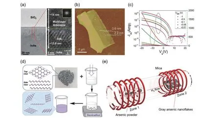
Scientists have been trying to prepare high quality arsenic crystal by using “top-down” exfoliation or to develop techniques to prepare arsenenes[12−14,17,18]. Tsaiet al. first reported multilayer arsenene nanoribbons on InAs substrate by using a plasma assisted processing (Fig. 2(a))[12]. The arsenene nanoribbons showed photoluminescence (PL)[9]. After that,Chenet al. and Zhonget al. discovered natural minerals of arsenic (orthorhombic crystal), which can be exfoliated into 2D arsenene nanoflakes (Fig. 2(b))[13,14]. Black arsenene shows anisotropy and semiconductive features (Fig. 2(c))[13,14]. However, obtaining gray arsenene by using mechanical exfoliation is difficult because of strong interlayer force. Qiet al. studied the interaction between arsenene and 14 solvents to find the optimal solvent for exfoliation (Fig. 2(d))[15]. Wanget al. exfoliated bulk arsenic crystals into nanoflakes by using DMSO as the solvent[16]. The arsenene nanosheets showed therapeutic effect to acute promyelocytic leukemia (APL)[16]. Huet al. prepared gray arsenene single-crystal nanoflakes on mica substrate (Fig. 2(e))[17]. Gray arsenene nanoflakes were transformed into vitreous arseneneviaa simple wet chemistry method[18]. The completely vitrified arsenene nanoflakes keep hexagonal shape, showing amorphous characteristic[18].The two-terminal device based on completely vitrified arsenene presented electrical field-controlled drain current[18].
安化集团公司将以此次表彰为契机,认真学习借鉴全国设备管理优秀单位先进经验,不断夯实设备管理基础,规范设备管理流程,积极推广应用先进的设备监测技术和装备,提升设备管理水平,为公司更好更快发展奠定坚实基础。
欺诈风险交易:本模型选取手机银行的历史安全事件积累的5000 条报文作为业务欺诈报文作为基于异常序列的潜在业务欺诈智能预警模型中异常交易的测试集。
In short, arsenene is an interesting material with anisotropy, considerable carrier mobility and obvious PL. It may find applications in functional devices.

Fig. 1. (Color online) Crystal structures, Brillouin zones, phonon spectra and electrical band structures of (a) puckered and (b) buckled arsenenes.Reproduced with permission[6], Copyright 2015, American Physical Society. (c) Electrical band structures of buckled arsenene with different layer numbers. Reproduced with permission[7], Copyright 2015, Wiley-VCH. (d) Schematic illustration for double-gated MOSFET of arsenene. Reproduced with permission[9], Copyright 2016, Springer Nature.

Fig. 2. (Color online) (a) Cross-sectional image of arsenene grown on InAs substrate. Reproduced with permission[12], Copyright 2016, American Physical Society. (b) AFM image of black arsenene exfoliated from natural minerals. Reproduced with permission[13], Copyright 2018, Wiley-VCH.(c) Transfer characteristic of a monolayer black arsenene device. Reproduced with permission[14], Copyright 2018, Wiley-VCH. (d) Schematic illustration for liquid-phase exfoliation of arsenene from bulk gray arsenic crystals. Reproduced with permission[15], Copyright 2016, Royal Society of Chemistry. (e) Schematic illustration for growth of gray arsenene nanoflakes on mica. Reproduced with permission[17], Copyright 2019, American Chemical Society.
Acknowledgements
This work was supported by the National Key Research and Development Program of China (2017YFA0208200), the Fundamental Research Funds for the Central Universities of China (0205-14380266), the National Natural Science Foundation of China (22022505 and 21872069), the Natural Science Foundation of Jiangsu Province (BK20180008), and the Shenzhen Fundamental Research Program of Science, Technology and Innovation (JCYJ20180307155007589). L. Ding thanks the National Key Research and Development Program of China(2017YFA0206600) and the National Natural Science Foundation of China (51773045, 21772030, 51922032, 21961160720)for financial support.
猜你喜欢
杂志排行
Journal of Semiconductors的其它文章
- T unable crystal structure of Cu–Zn–Sn–S nanocrystals for improving photocatalytic hydrogen evolution enabled by copper element regulation
- I nstability of parasitic capacitance in T-shape-gate enhancementmode AlGaN/GaN MIS-HEMTs
- Structural, optical and antimicrobial properties of pure and Agdoped ZnO nanostructures
- Performance enhancement of solution-processed InZnO thin-film transistors by Al doping and surface passivation
- T he origin and evolution of Y6 structure
- Star perovskite materials
