Ultra wideband CMOS digital T-type attenuator with low phase errors
2022-03-24ChaoFanYahuaRanandLiqunYe
Chao Fan, Yahua Ran, and Liqun Ye
Chengdu CORPRO technology Co., Ltd., Chengdu 610000, China
Abstract: A proposed inductive-phase-compensation ultra wideband CMOS digital T-type attenuator design based on an analysis of minimising phase errors is presented in this letter. In a standard CMOS technology, the proposed attenuator is analytically demonstrated to have low phase errors due to the inductive-phase-compensation network. A design equation is inferred and a wide-band 4dB attenuation bit digital attenuator with low phase errors is designed as a test vehicle for the proposed approach.
Key words: ultra-wideband; digital T-type attenuator; low phase error; inductive-phase-compensation; CMOS
1.Introduction
Digital attenuators are widely used in phased-array radars, modern wireless communications systems[1], temperature compensation and the automatic gain control scheme for transmitter/receiver systems. Previously, various digital attenuators are realized by employing several circuit structure with different circuit devices for switching[2−9], the T-type attenuator is investigated here, as it has advantage of compact footprint and low insertion loss of a reduced number of series switches. In Ref. [2], a low-pass filter that made up of one series inductor or shunt capacitor and two resistors are adopted in the typical switched T attenuator to minimize phase errors. But an extra filter increases the chip area and degrades the insertion loss. In Refs. [4–8], a phase-compensated capacitorCcis parallel/serial connected with a shunt resistorRpfrom the attenuating path, the T-type attenuator achieves low phase errors between the reference state and attenuating state, while maintaining the insertion loss. However, these capacitive-phase-compensation T-type digital attenuator designs commonly have poor design accuracy, since the manufacturing tolerance of capacitors is normally 5%–10% in a standard CMOS technology[10]. A novel ultra wideband CMOS digital T-type attenuator with low phase errors is presented in this paper. The proposed CMOS digital attenuator adopting a novel inductive-phase-compensation network which is designed in the attenuating path is introduced in the typical switched T attenuator topology to correct the phase errors without compromising the chip footprint and the insertion loss. And the inductive-phase-compensation T-type digital attenuator designs have satisfying design accuracy, since the inductorsLsare better modeled using electromagnetic simulation software.
2.Circuit design
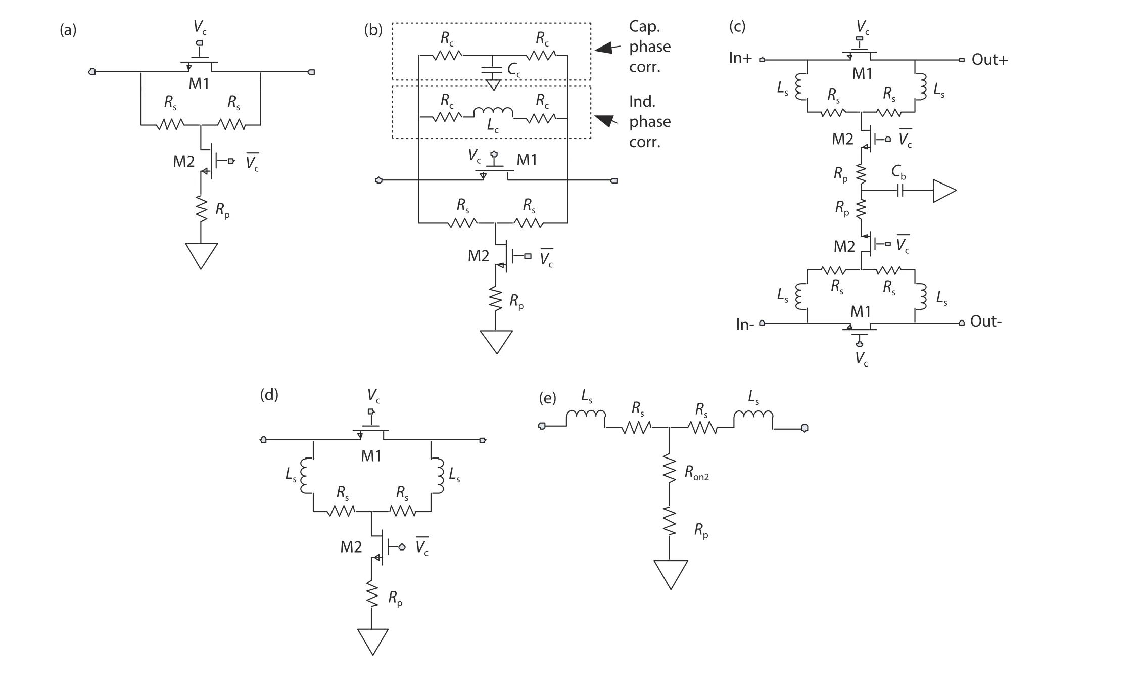
Fig. 1 shows several different structures of switched T digital attenuator. Fig. 1(a) shows that the typical switched Ttype attenuator use switches to transform the signal path between the reference state (switch M1 is on and M2 off) and attenuating state (switch M1 is off and M2 on). By analyzing the circuits in Fig. 1(a), it is easy to deduce that a phase error occurs between the reference states and the attenuation states which is produced by turn-off capacitanceCoff1of the switches. As this unwanted phase errors are significant in phased-array radars, it is necessary to reduce the phase error.In Fig. 1(b), a low-pass filter that made up of one series inductor or shunt capacitor and two resistors is adopted in the typical switched T attenuator to minimize phase errors. But an extra filter increases the chip area and degrades the insertion loss.
Fig. 1(c) illustrates a proposed inductive-phase-compensation CMOS differential T-type attenuator. By serial connecting a phase-compensated inductorLswith a resistorRsfrom the signal attenuating path, the proposed attenuator achieve a low phase errors between the reference state and attenuating state, while maintaining the insertion loss. As shown in Fig. 1(d), inductive-phase-compensation CMOS single-ended attenuator is half of the differential attenuator. The switch circuit model approximately equivalent to a on-state resistorRonand off-state capacitorCoffbecause of neglecting the parasitic parameters by using a simple analysis. By changing a pair of the opposite voltages on the gate of the MOS device,the reference state and the attenuating state can be obtained respectively. In the attenuating state, two inductorsLsare added in the attenuating path for phase compensation network. And the network can be illuminated using a T-type low-pass filter, as shown in Fig. 1(e).Thus, the insertion loss phase difference between the reference state and attenuating state can be effectively reduced by using the phase-lag characteristic of a low-pass filter.
By analyzing the circuits in Fig. 1(e), the equation of transmission phase of the compensation network can be derived as:


Fig. 1. Structures of switched T digital attenuator. (a) Typical switched T attenuator. (b) Capacitance/Inductive-phase-compensation T-type attenuator. (c) Structures of the proposed T-type digital differential attenuator. (d) Structures of the proposed T-type digital single-ended attenuator.(e) Phase compensation network.

Fig. 2. (a) (Color online) The die of the proposed switched T attenuator. (b) Simulated and measured insertion loss phases of reference and attenuating states and phase errors of proposed switched T attenuator. (c) Simulated and measured IL of reference and attenuating states and relative attenuation of proposed switched T attenuator

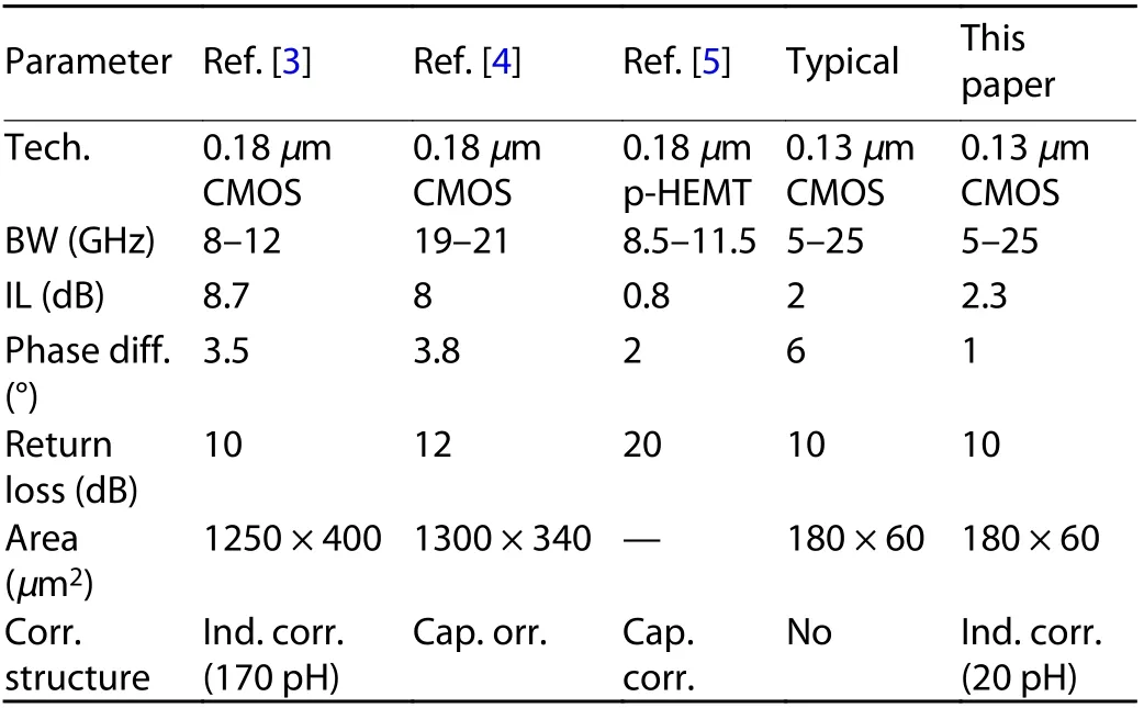
Table 1. Comparison of attenuation 4 dB bit attenuators.
whereωis the working frequency of the proposed T-type attenuator.
As Eq. (1) shows, the proposed inductive-phase-compensation network has a low-pass characteristic. Therefore, the insertion loss phase errors of the T-type attenuator between the reference state and attenuating state can be effectively reduced by optimising the design of low pass filter units, while maintaining the attenuation.
The proposed ultra wideband CMOS digital T-type attenuator was measured using an on-wafer probing system. It was measured with an Agilent N5242A PNA-X Vector Network Analyzer to a Cascade Microtech probe station. The proposed inductive-phase-compensation CMOS 4 dB bit digital T-type attenuator is shown in Fig. 2(a), which was employing the 0.13-μm CMOS process.
Fig. 2(b) shows the simulated and measured insertion loss phases results of the proposed attenuator, the simulated phase errors is only 0° to +0.8° ranging from 5 to 25 GHz. And the measured phase errors are only –1° to 0° during the 5–25 GHz operating range, which is close to the simulation results.Table 1 gives a comparison of several different compensated 4 dB bit attenuator cell performance. Compared to the design in Ref. [5], the proposed designs generally have satisfying design accuracy that the phase variation is only 1°, as the inductorsLsare better modeled using electromagnetic simulators. And the proposed design has a more compact footprint than the design in Ref. [3], because of the corr. structure inductor (Ls≈ 20 pH) is about one-eighth of in Ref. [3].
Fig. 2(c) shows simulated and measured insertion loss of reference and attenuating states and relative attenuation of proposed attenuator. And its’ insertion loss can maintain the<2.3 dB over a frequency of 5–25 GHz. The input 1 dB compression point and the return loss are better than 18 dBm and 10 dB ranging from 5 to 25 GHz, respectively.
3.Conclusion
In summary, A novel ultra wideband CMOS digital T-type attenuator with low phase errors is presented in this paper. A novel inductive-phase-compensation network is designed in the attenuating path of the typical switched T attenuator topology, to correct the phase errors without compromising the chip footprint and the insertion loss. And the proposed Ttype CMOS attenuator with a compact footprint design indicates a satisfying accuracy, as the inductors (Ls≈ 20 pH) are better modeled using electromagnetic simulators. The proposed T-type CMOS attenuator can maintain <2.3 dB insertion loss while achieving a 1° of phase errors over 5–25 GHz, which support the theoretical analysis.
杂志排行
Journal of Semiconductors的其它文章
- T unable crystal structure of Cu–Zn–Sn–S nanocrystals for improving photocatalytic hydrogen evolution enabled by copper element regulation
- I nstability of parasitic capacitance in T-shape-gate enhancementmode AlGaN/GaN MIS-HEMTs
- Structural, optical and antimicrobial properties of pure and Agdoped ZnO nanostructures
- Performance enhancement of solution-processed InZnO thin-film transistors by Al doping and surface passivation
- T he origin and evolution of Y6 structure
- Star perovskite materials
