Van der Waals two-color infrared photodetector
2022-03-15PeisongWuLeiYeLeiTongPengWangYangWangHailuWangHaonanGeZhenWangYueGuKunZhangYiyeYuMengPengFangWangMinHuangPengZhouandWeidaHu
Peisong Wu,Lei Ye ,Lei Tong,Peng Wang,Yang Wang,Hailu Wang,Haonan Ge,Zhen Wang,Yue Gu,Kun Zhang,Yiye Yu,,Meng Peng,,Fang Wang,Min Huang,Peng Zhouand Weida Hu ✉
1State Key Laboratory of Infrared Physics,Shanghai Institute of Technical Physics,Chinese Academy of Sciences,Shanghai 200083,China
2University of Chinese Academy of Sciences,Beijing 100049,China
These authors contributed equally:Peisong Wu,Lei Ye,Lei Tong
Abstract With the increasing demand for multispectral information acquisition,infrared multispectral imaging technology that is inexpensive and can be miniaturized and integrated into other devices has received extensive attention.However,the widespread usage of such photodetectors is still limited by the high cost of epitaxial semiconductors and complex cryogenic cooling systems.Here,we demonstrate a noncooled two-color infrared photodetector that can provide temporal-spatial coexisting spectral blackbody detection at both near-infrared and mid-infrared wavelengths.This photodetector consists of vertically stacked back-to-back diode structures.The two-color signals can be effectively separated to achieve ultralow crosstalk of ~0.05% by controlling the built-in electric field depending on the intermediate layer,which acts as an electron-collecting layer and hole-blocking barrier.The impressive performance of the two-color photodetector is verified by the specific detectivity(D*)of 6.4×109 cm Hz1/2 W-1 at 3.5 μm and room temperature,as well as the promising NIR/MWIR two-color infrared imaging and absolute temperature detection.
Introduction
Two-color infrared(IR)technology can identify targets in a complex environment by using the multispectral features of targets,and this technique has been widely used in information technology,life sciences,aerospace,and other fields1-5.As this technology has been developed,the main research direction has become the integration of two-color detection into single pixels without complex optical components6while solving the core problem of separating and detecting dual spectral information independently7.Early techniques for obtaining the information from two bands involved a photodetector unit composed of multiple pixels with different response spectra in the plane,but poor spatial consistency led to aberrations in imaging.In 1980,a structure based on a back-to-back concept with three electrodes was designed8to solve the problem of spatial coexcitation,but this strategy results in poor temporal coherence during sequential detection,which makes it very difficult to detect a moving target9.Since then,the simultaneous temporal-spatial mode of two-color IR photodetectors has been a popular research topic and has been successfully implemented in HgCdTe(MCT)10,quantum wells11,type II superlattices12and so on.However,these conventional two-color IR photodetectors require complex cryogenic cooling systems to reduce dark current13,and their activelayer materials are more or less facing lattice mismatch at the interface in the process of multilayer heteroepitaxy,against the requirement of low-crosstalk and miniaturization applications7.Therefore,there is much interest in new IR materials and structures that fill gaps in the existing field.
Two-dimensional(2D)materials have shown infinite potential for use in future IR photodetectors14-17.Different from conventional thin-film materials,layered 2D materials exhibit van der Waals(vdWs)bonding18and can therefore be stacked in any number of layers regardless of lattice mismatching19,the deposition temperature and dangling surface bonds20,which makes them promising for integration with mature 3D material systems21-26.Therefore,the band at the interface of the vdWs heterojunction can change abruptly with sharp band edges,which makes it possible to assemble devices with well-designed bands27,28.More importantly,layered 2D materials do not incur defects induced by internal stress29;therefore,the dark current induced by crystal surface defects and thermal ionization is reduced,indicating high potential for use in IR photodetection at room temperature30-34.Here,we designed a vertically stacked back-to-back 2D/3D hybrid photodetector with a black phosphorus(bP)/molybdenum sulfide(MoS2)/silicon(Si)vdWs heterostructure for use in temporal-spatial coexisting NIR/MWIR two-color blackbody sensitive photodetectors with ultralow crosstalk of ~0.05%at room temperature.Two built-in electric fields with opposite directions were successfully introduced by constructing a p-n-p-junction with a back-to-back structure,achieving the separation and detection of photogenerated carriers in two bands.Finite-element simulation was also utilized to optimize the band structure to reduce optical and electrical crosstalk.We demonstrated absolute temperature detection and IR imaging in two colors,indicating the reliability and application prospects of vdWs heterojunctions based on silicon technology in two-color photodetection.
Results
Design of the van der Waals two-color infrared photodetector
A diagram of a two-color photodetector with a p-n-p structure is shown in Fig.1a.P-type bP was combined with n-type MoS2to form a bP/MoS2p-n junction for MWIR detection;the bP/MoS2p-n junction was transferred onto the etched window of p-type thin-film Si to form a MoS2/Si n-p junction for NIR detection,resulting in a vertical vdWs heterostructure of bP/MoS2/Si.The vdWs heterostructures were built by the dry transfer method35with mechanical stripping and stacking.More details of the fabrication can be found in the Methods section and Supplementary Information.Operating under back irradiation conditions,the photodetector performance was measured by using the circuit configuration shown in Fig.1b.In its vertical structure,n-type MoS2plays the role of electron collection and hole barrier layer,while p-type Si and bP are used to absorb NIR and MWIR radiation,respectively,resulting in spatially consistent two-color detection.Under NIR illumination,photogenerated electron-hole pairs are separated by the built-in electric field(E1)of the MoS2/Si heterojunction,pushing electrons to flow through the electrode via MoS2and holes to flow through the electrode via p-Si,while the same processes occur at the bP/MoS2heterojunction under MWIR radiation.Figure 1e shows the simulated band diagram of bP/MoS2/Si with p-Si applied at a negative voltage,suggesting that its key advantage is generating and collecting photogenerated holes in the NIR and MWIR bands independently at the junctions of Si/MoS2and bP/MoS2,respectively.This leads to little electrical crosstalk.A pseudocolor transmission electron micrograph(TEM)of a completed device is shown in Fig.1c,d.The layered characteristics of bP and MoS2are obvious,with the intervals of a single layer being 5.5 and 6 Å,respectively.The high-resolution TEM images show that the interface between the bp/MoS2atomic layers was clean without any contamination or amorphous oxide being generated during the fabrication.Because bP is easily oxidized,we also measured oxygen at the bp/MoS2interface,and EDS mapping results showed no oxygen or organic matter(Fig.S3a).The whole process involving the device was carried out in a nitrogen glove box,so almost no oxide layer or organic matter was present at the Si/MoS2interface(Fig.S3b),which greatly improved the performance of the device.
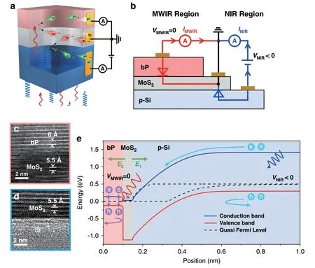
Fig.1 BP/MoS2/Si van der Waals two-color infrared detector concept.a Schematic of van der Waals two-color infrared photodetector,showing the working mode and external circuit of the photodetector.b Circuit configuration of device to demonstrate the performance of two-color photodetector.c Cross-sectional TEM image showing the bP/MoS2 interface.d Cross-sectional TEM image showing the Si/MoS2 interface.e Simulated energy band diagram with p-Si applied a negative voltage
Two-color performance characterization
We separately evaluated the bP/MoS2heterojunction of the photodetector with MWIR irradiation and the MoS2/Si heterojunction with NIR irradiation.TheI-Vcurve characteristics of the bP/MoS2heterojunction without illumination at 300 K are shown in Fig.2a,illustrating a typical rectification characteristic of the p-n junction.The inset of Fig.2a displays the relation between current density and voltage(J-Vcurves)under dark and 1200 K blackbody illumination,revealing a typical photovoltaic mode for the MWIR photoresponse.Figure 2b shows theI-Vcurve characteristics of the MoS2/Si heterojunction without illumination at 300 K.As a reverse bias voltage is applied,E1is strengthened,and the depletion region is enlarged.The inset of Fig.2b shows theJ-Vcurves of the MoS2/Si heterojunction under dark conditions and 1200 K blackbody illumination at negative bias.
whereInis the noise current,Ris the responsivity,Ais the effective area of the photodetector,and Δfis the bandwidth.The noise current is dominated by several types of noise,including Johnson noise,shot noise and background fluctuation-induced noise.To date,no IR photodetector operating at room temperature can reach the performance limit of background fluctuation;therefore,the background fluctuation-induced noise can be neglected.However,the dominant source of noise current is different for our photodetector with two operating modes.
In MWIR band detection,the dominant noise in the photodetector is Johnson noise because there is no additional driving power.In this method,the calculation for photodiodes with zero bias usually requires the extraction of zero-bias resistanceR0(extracted from theI-Vmeasurements)36:

where η is the external quantum efficiency,λ is the wavelength,qis the elementary charge,his the Planck constant,cis the speed of light,kis the Boltzmann constant,Tis the photodetector temperature,andR0is the zero-bias resistance.From this,of the MWIR photodetection at 1200 K blackbody is calculated to be 1.78×109cm Hz1/2W-1.
For NIR,the noise in the photodetector under reverse bias is dominated by shot noise(much greater than Johnson noise)36.D*Rcan be calculated by:

whereIDis the dark current.Therefore,the calculatedof the NIR photodetector with a 1200 K blackbody is 9.8×108cm Hz1/2W-1.D*of the device decreases with decreasing blackbody temperature,as shown in Fig.2c.This is due to the redshift in the peak wavelength caused by the decrease in the blackbody temperature,and the radiation power is greatly reduced.
We further conducted spectral photoresponse measurements at room temperature for the two-color IR photodetector,as shown in Fig.2d,with a Fourier transform IR(FTIR)spectrometer and grating spectrometer.The cut-off wavelengths in the NIR and MWIR ranges were 0.9 and 3.9 μm,respectively.The peak detectivity in the MWIR range was 6.4×109cm Hz1/2W-1at 3.5 μm(Fig.S6c)and was almost constant despite blackbody temperature changes,showing good stability and adaptability(Fig.2c).TheD*(λ)of the photodetector is comparable to that of commercialized noncooled NIR/MWIR two-color photodetectors,which indicates the application prospects of 2D vdWs heterostructures for use in IR photodetectors operating at room temperature(Fig.2e).Figure S7 shows the measured noise current spectra of MWIR and NIR.According to the directly measured noise,the D* values calculated according to Eq.(1)were 3.51×109cm Hz1/2W-1(MWIR at 3.5 μm)and 3.34×108cm Hz1/2W-1(NIR),respectively.In this value,D*calculated fromIdandR0has good consistency.Moreover,the monochromatic photoresponse and low-temperature performance of the device was verified by the laser.The detailed information can be found in Fig.S9.Figure S8 shows the response time of the detector in microseconds and the linear dynamic range greater than 70 dB.

Fig.2 Two-color performance characterization and colorimetric temperature measurement.a Dark current characteristics of bP/MoS2 heterojunction photodiode in 300 K without illumination.Inset:the J-V characteristics of the device with or without a 1200 K blackbody source.b Dark current characteristics of Si/MoS2 heterojunction photodiode in 300 K without illumination.Inset:the J-V characteristics of the device with or without a 1200 K blackbody source.c Specific detectivity at different blackbody temperatures.d Normalized spectral response of the two-color photodetector during the back radiation.The 0.7-1.3 μm of the spectrum was measured by a grating spectrometer.The 1.3-4.5 μm of the spectrum was measured by FTIR.All FTIR and laser diode characterization were performed at a bias of 0 V(MWIR)and -0.5 V(NIR).e Specific detectivity as a function of wavelength measured for a bP/MoS2/Si heterojunction at room temperature as well as various commercially available and reported NIR/MWIR two-color photodetectors,including MCT/Si(Kunming Institute of Physics),InGaAs/Si(Hamamatsu K1713-08)and InAsSb/Si(Hamamatsu K1713-003).All FTIR and laser diode characterization was performed at a bias of 0 V.The black line in the figure is the performance limit of photovoltaic devices;the red line is the performance limit of thermoelectric device;the gray box is commercial thermistor.f Left axis,NIR and MWIR signals as a function of photodetector-blackbody distance.Right axis,the relationship between the NIR/MWIR ratio and photodetector-blackbody distance.g NIR/MWIR ratio depends on the blackbody temperature.Red dots show the measured NIR/MWIR ratio in each blackbody temperature
Colorimetric temperature measurement
Two-color IR photodetectors are widely used for temperature measurement and provide more reliable and accurate detection than single-band photodetectors2.With increasing object temperature,the radiation intensity over the whole spectrum increases,and the peak shifts to shorter wavelengths,as shown by Planck’s law(Fig.S5a).According to Planck’s law under the Wien approximation,the monochromatic emission power M is:

where ε is the emissivity,his the Planck constant,cis the light speed,λ is the wavelength,Δλ is the wavelength width,kis the Boltzmann constant,andTis the photodetector temperature.For single temperature measurements,information on the emissivity and distance to the heat source is needed to determine the temperature of the object.However,in real measurements,the emissivity and distance to the heat source are often unknown.A two-color temperature measurement can eliminate the error associated with emittance and distance.Two-color temperature measurement is based on the ratio of two adjacent wavelengths of the IR radiation energyRto determine the temperature of the target object:
信息技术与课程整合的研究现状 笔者查阅相关文献发现,我国关于信息技术与课程整合的方法与实施策略的研究仍比较薄弱,很多中小学教师以及教育工作者不清楚信息技术与课程整合的模式、方法、实施策略等,在实际教学中不知道如何进行整合实践;而且目前的研究多数是将传统的教学模式和信息技术与课程整合的模式进行比较分析,鲜有研究把信息技术与课程整合的几种模式进行内部比较,这也是资源、设施的应用率比较低的原因之一。

whereC1andC2are the system constants.The reason for selecting adjacent wavelengths is that the epsilon of the adjacent wavelength of the emissivity rate is roughly the same;under certain conditions ε1/ε2,at the same time,and under the same detection range,its radiation power attenuation ratio is approximately the same.Therefore,the two-color photodetector can measure the absolute temperature by using the dual band information,regardless of the distance and emittance of the object,as shown in the schematic diagram of the temperature measurement setup in Fig.S4.Distance-dependent performance testing was performed to verify the influence of emission and radiation power attenuation at various distances on signal detection,and the result is shown in Fig.2f.The NIR/MWIR signal ratio is almost a constant for a given temperature,independent of the radiation power and distance,so the value can correspond to the absolute temperature of the target at any distance.In addition,we varied the target temperature to verify the performance,as shown in Fig.2g,revealing the corresponding relationship between the NIR/MWIR signal ratio and temperature.The signal ratio increased from 0.018 to 0.45 as the blackbody temperature increased from 850 to 1200 K.The temperatures of heat sources A and B were 923 and 1123 K,respectively,and the corresponding ratios obtained by the photodetector were 0.068 and 0.25.According to the fitting curve in Fig.2g,corresponding ratios of 0.068 and 0.25 were calculated,and the detection temperatures were 930 and 1132 K,respectively,with the error being within the allowable range of the system.These results show that the two-color photodetector can remotely measure the temperature of a target heat source on the basis of the response ratio.Figure S5b shows the relationship between blackbodyD*and radiant power.Under the same blackbody temperature,theD*of the device did not change with the change in blackbody radiation power.The operating frequency of the two-color photodetector reached 200 Hz,while the NIR/MWIR ratio remained constant,as shown in Fig.S12a.The repeatability of the measurement is shown in Fig.S13.
Crosstalk simulation and characterization
For distinguishing signals,crosstalk is an important index of a two-color photodetector.The crosstalk in a two-color photodetector consists of optical crosstalk and electrical crosstalk7.Optical crosstalk refers to the response of the MWIR layer to NIR light that is not fully absorbed by the NIR absorption layer.Electric crosstalk refers to the nonequilibrium carrier diffusion between the two absorption layers.Specifically,there are two kinds of crosstalk in this device.CNIRtoMWIR(crosstalk of NIR to MWIR)is defined as the signal ratio of two junction signals of the NIR photodetector under MWIR radiation,which is mainly caused by electric crosstalk.CMWIRtoNIR(crosstalk of MWIR to NIR)is defined as the signal ratio of the MWIR photodetector under NIR radiation,which is mainly caused by combined optical and electric crosstalk(Fig.S14).

For electric crosstalk,the electric field distribution and photocurrent distribution were studied by finite-element simulations.Different doping concentrations of Si can affect the internal electric field distribution.The band diagram for heavy Si doping is shown in Fig.3a,and theCNIRtoMWIRfor heavy Si doping under the same conditions was very large.Figure 3b shows that the heavily doped Si/MoS2depletion region was mainly distributed in MoS2,leading to overlap of the two depletion regions,and the signal generated by the MWIR junction was received by both the MWIR and NIR electrodes.These test results show that the crosstalk could not be suppressed,as shown in Fig.3c.For light Si doping(1015cm-3),the band diagram is shown in Fig.3d.The depletion regions of the NIR and MWIR photodiodes were distributed in Si and bP,respectively(Fig.3e).The depletion region was effectively blocked by the intermediate layer,which formed a barrier to block photogenerated holes,resulting in ultralow electrical crosstalk in the device(Fig.3f).Therefore,MWIR-to-NIR crosstalk of 1.2% and NIR-to-MWIR crosstalk of 0.05%were obtained from Eqs.(7)and(8),respectively.
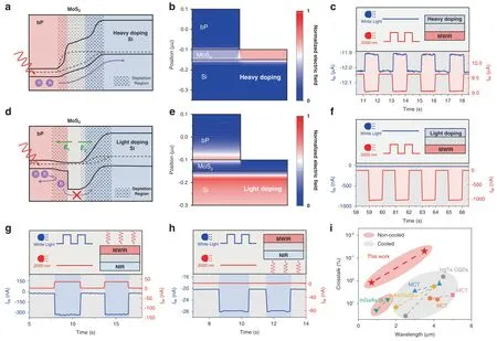
Fig.3 Ultralow crosstalk in bP/MoS2/Si two-color IR photodetector.a Band diagram and depletion region distribution of heavily doped Si twocolor devices in working mode.b Electric field distribution of heavily doped Si two-color devices in working mode.c Photocurrent of heavily doped Si two-color photodetector under a modulated illumination source(λ=2 μm).Red and blue line are MWIR and NIR photocurrents,respectively.d Band diagram and depletion region distribution of light doped Si two-color devices in working mode.e Electric field distribution of light doped Si two-color devices in working mode.f Photocurrent of light doped Si two-color photodetector under a modulated illumination source(λ=2 μm).g Photocurrent of light doped Si two-color photodetector under a modulated illumination source(White light)in front radiation mode.h Photocurrent of light doped Si two-color photodetector under a modulated illumination source(White light)in back radiation mode.i Crosstalk performance of bP/MoS2/Si devices and various reported two-color photodetectors
The optical crosstalk was analysed by white light irradiation in front irradiation mode and back irradiation mode.In front irradiation mode,the MWIR device absorbed white light directly,so there was considerable optical crosstalk(Fig.3g).The two-color photodetector in this paper used back irradiation,in which NIR absorber materials effectively absorbed NIR radiation and greatly reduced the optical crosstalk(Fig.3h).Compared with the frontal incident mode,theCMWIRtoNIRdecreased from 11.24% to 1.2% by integrating over the spectral coincidence area,as shown in Fig.S11a.To further verify the low crosstalk of the vdWs two-color photodetector,we compared the crosstalk in our device with that in other structures.Figure 3i shows the comparison of the twocolor crosstalk in the vdWs two-color photodetector(red line)and commercial devices.The vdWs two-color photodetector exhibited ultralow two-color crosstalk compared to the integrated two-color photodetector based on conventional materials.
Temporal-spatial coexisting two-color IR imaging
After calibrating the temperature recognition function of the device,a two-color imaging experiment was carried out.A blackbody-like radiant heat source was used as the target to verify the two-color detection capability of our device37.Figure 4a displays a schematic diagram of the imaging setup,and the two-color photodetector was used to replace the detecting chip of a camera.An image was acquired by two-dimensional scanning and converting the output voltage of each pixel into a gray value.Two output channels were used to ensure the simultaneous acquisition of both bands in the imaging.To better understand the two-color performance,we constructed a complex scene in which a Si wafer was placed in front of the heat target,as shown in Fig.4b,c.Two opposite built-in electric fields can detect the photogenerated carriers from the two bands independently,which was enabled by the vertical structure.The photodetector showed high temporal and spatial consistency in the two-color detection.The NIR and MWIR imaging results were captured as shown in Fig.4d,e.Here,the results are attributed to the high dynamic range imaging capability of the two-color photodetector,which is a key feature of high-quality imaging.On the other hand,the lower half of the target was not detected because the light does not penetrate Si,as shown in the NIR imaging results(Fig.4d).Therefore,in a complex environment,a twocolor photodetector can obtain more target information than single-color imaging and detect the temperature of the target at the same time as two-color imaging.The photocurrentsINandIMwere extracted from the twocolor image,and the signal ratio of the heating tube was 0.625.Based on Fig.3c,the temperature of the heating tube was ~1257 K,which was very close to the actual temperature of 1300 K.Interestingly,commercial handheld IR thermometers could not identify the internal temperature of the resistance wire because the glass shell of the heating tube blocked the heat emitted by the carbon fiber heating wire(Fig.S17).These results show that a two-color image can provide more information than a single-band image.

Fig.4 Temporal-spatial coexisting two-color IR imaging.a Schematic diagram of simultaneous mode two-color imaging system.Inset:optical image of two-color vdWs infrared photodetector.b Photograph of target(carbon fiber heating tube)was captured by a silica-based camera.c Photograph of target(carbon fiber heating tube covered by silicon wafer)was captured by a silica-based camera.d NIR images of objects behind a silicon wafer.The black dotted circle marks the position of the silicon wafer.The white dotted box indicates the location of photocurrent IN extraction.e MWIR images of objects behind a silicon wafer.The white dotted circle marks the position of the silicon wafer.The white dotted box indicates the location of photocurrent IM extraction
Discussion
In this study,we systematically investigated vdWs heterostructure-based multispectral detection to design and fabricate a two-color IR photodetector based on the p-n-p-vertical structure of bP/MoS2/Si and found impressive room-temperature specific detectivityD*of 6.4×109cm Hz1/2W-1at 3.5 μm under blackbody radiation.The photogenerated carriers in two bands are successfully separated by two opposite built-in electric fields.The ultralow crosstalk of 1.2% for MWIR-to-NIR and 0.05%for NIR-to-MWIR due to the filtering effect of thinfilm Si and the barrier effect of MoS2ensures the independent readout of the dual band information.Moreover,calibration of the response under both the NIR and MWIR bands can be used to determine the absolute temperature of a heat source regardless of the detection distance and emissivity.Simultaneous imaging of the NIR and MWIR bands and imaging temperature detection were demonstrated.Compatible with existing silicon technology,vdWs heterojunctions can enable roomtemperature IR two-color detection because of their novel device structure and energy band design,which is expected to improve current multispectral IR detection technologies.
Methods
Device fabrication
The bP/MoS2/Si vdWs heterostructure was fabricated by the dry transfer method.The 2D materials were mechanically exfoliated from bulk materials supplied by Smart Elements,HQ graphene.A detailed description of this process is provided in Supplementary Section 1.The exfoliation and transfer processes were carried out in a N2-protected glovebox to decrease the oxidation of the material.Electrode contact was defined using electron beam lithography,and Cr/Au(15/80 nm)was deposited using thermal evaporation.Before measurement,a thin PMMA layer was coated to protect the device from exposure to air and water.
Photodetector performance
The simulation structure consisted of a 200 nm p-type black phosphorus layer,a 50 nm n-type MoS2layer,and a 200 nm p-type Si layer.The doping concentrations were assumed to be 5×1015cm-3black phosphorus,1×1017cm-3MoS2,1×1018cm-3Si(high doping),and 1×1015cm-3Si(low doping).The electronic characteristics were measured by an Agilent B2902A source.Blackbody testing was performed using a calibrated commercial blackbody furnace(HFY-206A).After the frequency was modulated by an optical chopper wheel,the photocurrent signal was converted into a voltage signal using a current preamplifier(Stanford Research Systems SR570)and recorded by a lock-in amplifier(Ametek Model 7270 DSP).The laser spectral response test was carried out by a combination of a continuous laser light source(YSL sc-pro)and gratings.The IR spectrum test adopted in this experiment was carried out by an FTIR spectrometer(Nicolet 8700),and globar light(1000 K blackbody)was used as the internal light source at room temperature.In all the photocurrent measurements,the laser(2000 nm)was focused on the device through a fixed optical path using a 20× objective lens(NA=0.45)with a laser spot diameter of ~20 μm.The mid-IR laser responses of the photodetectors were tested by a mid-IR plasma laser with tuneable wavelengths(2.6,3.1,4,and 4.2 μm).The transient photocurrent response(at 2000 nm)was recorded using an oscilloscope(Tektronix DPO 5204)to analyse the photoresponse time.All measurements were performed at room temperature in an ambient environment.Electrical simulations were performed using the finite-element method.
Acknowledgements
This work was supported by the National Natural Science Foundation of China(Grant No.62122081,61905266,62134009,61725505,11734016,61974050),Youth Innovation Promotion Association CAS,and Fund of Shanghai Natural Science Foundation(Grant No.21JC1406100,19YF1454600 and 19XD1404100).
Author details
1State Key Laboratory of Infrared Physics,Shanghai Institute of Technical Physics,Chinese Academy of Sciences,Shanghai 200083,China.2University of Chinese Academy of Sciences,Beijing 100049,China.3Hubei Yangtze Memory Labs,School of Optical and Electronic Information and Wuhan National Laboratory for Optoelectronics,Huazhong University of Science and Technology,Wuhan,Hubei 430205,China.4State Key Laboratory of ASIC and Systems,School of Microelectronics,Fudan University,Shanghai 200433,China
Author contributions
W.H.,P.Z.,and P.W.conceived the project and designed the experiments.P.S.W.,L.Y.,and L.T.carried out most of the experiments and analysed the data.H.N.G.and Y.G.contributed to the theoretical calculations.Y.W.,Z.W.,M.P.,Y.Y.Y.,and F.W.analysed the data.Y.W.carried out the AFM measurements.K.Z.conducted the blackbody measurements.M.H.conducted the FTIR measurements.H.L.W.conducted the imaging measurements.W.H.was responsible for project planning.P.S.W.,P.W.,P.Z.and W.H.co-wrote the manuscript.All authors discussed the results.
Conflict of interest
The authors declare no competing interests.
Supplementary informationThe online version contains supplementary material available at https://doi.org/10.1038/s41377-021-00694-4.
猜你喜欢
杂志排行

Light: Science & Applications的其它文章
- Thermal photonics boosts radiative cooling
- Van der Waals two-color infrared detection
- Probing the orbital angular momentum of intense vortex pulses with strong-field ionization
- Microsphere-assisted,nanospot,non-destructive metrology for semiconductor devices
- Angular engineering strategy of an additional periodic phase for widely tunable phase-matched deep-ultraviolet second harmonic generation
- First Chinese ultraviolet-visible hyperspectral satellite instrument implicating global air quality during the COVID-19 pandemic in early 2020