Effect of heavy ion irradiation on the interface traps of AlGaN/GaN high electron mobility transistors
2022-03-12ZhengZhaoLin林正兆Ling吕玲XueFengZheng郑雪峰YanRongCao曹艳荣PeiPeiHu胡培培XinFang房鑫andXiaoHuaMa马晓华
Zheng-Zhao Lin(林正兆) Ling L¨u(吕玲) Xue-Feng Zheng(郑雪峰) Yan-Rong Cao(曹艳荣)Pei-Pei Hu(胡培培) Xin Fang(房鑫) and Xiao-Hua Ma(马晓华)
1School of Microelectronics,Xidian University,Xi’an 710071,China
2School of Mechano-Electronic Engineering,Xidian University,Xi’an 710071,China
3Institute of Modern Physics,Chinese Academy of Sciences(CAS),Lanzhou 730000,China
Keywords: gallium nitride,radiation effects,defects,pulse testing
1. Introduction
Gallium nitride (GaN) based devices are widely used in optoelectronics and power applications. In particular, Al-GaN/GaN high electron mobility transistors (HEMTs) are considered as excellent candidates for future power devices because high carrier concentration and electron mobility can be achieved with the two-dimensional electron gas (2DEG)produced by the polarization effect.[1-5]Because the displacement threshold energy of GaN is high, GaN has more effective anti-radiation properties than other semiconductor materials.[6,7]Therefore, AlGaN/GaN HEMTs have obvious advantages in environments with extremely high levels of radiation,in which radiation effects and long-term reliability are important concerns.
Since 2000,numerous studies have been conducted to investigate the effects of radiation on AlGaN/GaN HEMTs.[8,9]The defects introduced by proton,electron,neutron,and heavy ion irradiation at the gate metal/barrier layer interface cause the interface state charge or discharge effect,which shifts the threshold voltage to positive values. Additionally, these irradiation defects increase the probability of electrons crossing the barrier, which increases in the gate-leakage current. Furthermore, irradiation defects in the 2DEG channel layer can capture electrons, thus decreasing the 2DEG density and the saturated drain current.[10-15]
In space, the energy and fluence range of heavy ions are respectively<10 GeV and 105-107particles·cm-2/day.[16]Therefore, practical insights can be gained from studying the effects of heavy ion irradiation on devices. Heavy ions cause single event effects (SEEs), and permanent structural damage in device materials, thereby affecting the stability of the devices.[17-21]Since 2007, researchers have used heavy ions to simulate SEEs. Studies have demonstrated that GaN devices can tolerate high levels of radiation tolerance under total ionizing dose,and enhance low dose rate sensitivity and SEE irradiation.[22,23]Most studies are still focusing on the displacement damage. The degradation phenomenon was found to depend on the ion type,angle,circuit capacitance and manufacturing lot.[24]Microscopic damage can be observed in devices irradiated with heavy ions by using a transmission electron microscope. Sasakiet al.observed dislocation rings in devices that were irradiation with 18 MeV Ni ions, but observed no stripe tracks or defects in these devices.[25]Chenet al.demonstrated that prior total ionizing dose irradiation with gamma rays exacerbates the SEE of GaN devices induced by subsequent181Ta32+irradiation.[26]Huet al.were the first to report that209Bi ions create quasi-continuous tracks in Al-GaN/GaN HEMT devices.[27]To elucidate the mechanism of device damage caused by radiation, many studies have been conducted based on two-dimensional technology computeraided design(2D TCAD).[28]
AlGaN/GaN HEMTs are widely known to be extremely sensitive to surface states,and current collapse is a major factor affecting the RF performance of these devices.[29-31]However,the effect of radiation on the metal/AlGaN layer,specifically the interface traps,has rarely been studied in detail.
Suddenly varying voltages can trap and release surface states,and this forms a“virtual gate”that decreases the drain current, thus affecting device performance.[32,33]PulsedI-Vtesting is commonly used to measure the amount of current collapse by indirectly characterizing the surface state of the device. In this study,the radiation defects at the metal/AlGaN interface were characterized by pulsedI-Vtesting, and measurements were conducted before and after irradiation to determine the change in trap time constants.
2. Experiments
AlGaN/GaN HEMTs were processed at Xidian University in China. They were grown on sapphire substrates by metal organic chemical vapor deposition. Epitaxial growth was initiated with an AlN nuclear layer, which was followed by a 2 μm undoped GaN buffer and a 22-nmthick Al0.3Ga0.7N barrier. The ohmic contact comprising Ti/Al/Ni/Au (20/160/55/45 nm) was annealed at 850°C for 30 s under a nitrogen atmosphere. Schottky contact was realized with Ni/Au/Ni(45/100/20 nm). A 180-nm-thick Si3N4passivation layer was deposited. The gate length and width were 0.2 μm and 50 μm,respectively. A schematic cross section of the AlGaN/GaN HEMTs is shown in Fig.1.

Fig.1. Schematic cross-section of AlGaN/GaN HEMTs.
The irradiation experiments were performed at the Heavy Ion Research Facility in Lanzhou. To study the effect of heavy ion irradiation on the devices, AlGaN/GaN HEMTs were irradiated with181Ta32+at 2.1 GeV with a total fluence of 1×10⁸ions/cm2, 1×10⁹ions/cm2and 1×10¹⁰ions/cm2at room temperature. The devices were not biased during the irradiation process.
A Keithley 4200 semiconductor parameter analyzer was used to conduct the DC and pulsedI-Vmeasurements at Xidian University. From the test results, we extracted the maximum saturation current, threshold voltage, maximum transconductance, gate-leakage and current collapse to analyze the degradation in electrical properties caused by irradiation. The change in the density of defect states can be determined by comparing the current collapse of the device under different static bias voltages. By comparing the results of tests conducted at different pulse widths, the time constants of the radiation defects can be calculated indirectly.
3. Results and discussion
Figure 2 shows the transfer characteristics of the Al-GaN/GaN HEMTs before and after the heavy ion irradiation.The threshold voltage (Vth) and maximum transconductance(Gmax)gradually degraded as the fluence increased.After irradiation by181Ta32+at a fluence of 1×10¹⁰ions/cm2,the electrical characteristics obviously degraded:Vthshifted positively by approximately 25%andGmaxdecreased by approximately 8%. Transconductance represents the gate control capability of the device and is an important parameter that affects the frequency characteristics. The degradedGmaxvalue can be used to evaluate the extent of damage in the gate area and the decrease in channel electron mobility. Therefore, after heavy ion irradiation, both the gate control capability of the device and the carrier mobility decreased slightly.
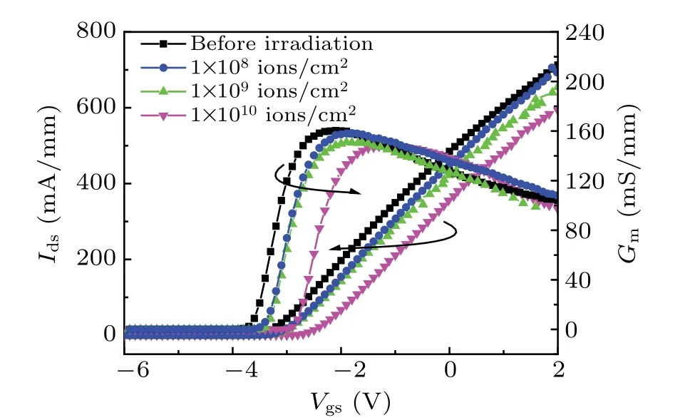
Fig.2. Transfer characteristics of AlGaN/GaN HEMTs before and after heavy ions irradiation at Vds =10 V.The heavy ions radiation dose varies from 1×10⁸ ions/cm2 to 1×10¹⁰ ions/cm2. The left y-axis is drain current,and the right y-axis is transconductance(Gm).
The output characteristics obtained before and after irradiation are shown in Fig.3. The maximum saturation current(Idsat) before and after irradiation by heavy ions with a fluence of 1×10¹⁰ions/cm2atVgs=2 V were 782 mA/mm and 672 mA/mm, respectively. The maximum saturation current was likely degraded by a decrease in electron concentration and saturated carrier velocity.

Fig. 3. The output characteristics of AlGaN/GaN HEMTs before and after heavy ions irradiation. The heavy ions radiation dose varies from 1×10⁸ ions/cm2 to 1×10¹⁰ ions/cm2. The applied gate bias varies from-6 V to 2 V,and the step is 1 V.
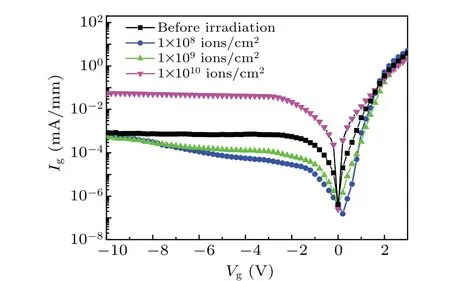
Fig. 4. Gate-leakage of AlGaN/GaN HEMTs before and after the heavy ions irradiation. The heavy ions radiation dose varies from 1×10⁸ ions/cm2 to 1×10¹⁰ ions/cm2.
Figure 4 displays the gate-leakage characteristics of the AlGaN/GaN HEMTs before and after irradiation. The results revealed that the gate-leakage currents were slightly improved at the fluences of 1×10⁸ions/cm2and 1×10⁹ions/cm2. This may be attributed to the interaction between181Ta32+and the lattice atoms, which releases a large amount of heat and produces an effect that is similar to thermal annealing, thereby improving the device performance at low fluences. However,other reports stated that it is due to the Kirkendall effect, an increase in the oxygen content at the AlGaN surface after irradiation, which creates a potential barrier for electrons, thus reducing the gate-leakage current.[34,35]At the high fluence of 1×10¹⁰ions/cm2, we observed a significant increase in the gate-leakage current, which maybe caused by the appearance of leakage paths at the interface between the gate metal and barrier layer. The gate forms a Schottky contact, and the Schottky barrier height and ideal factor can be calculated from the forwardIg-Vgcharacteristics. The barrier height is expressed as follows:

From the results shown in Table 1, the Schottky barrier height remained almost unchanged after irradiation. However, the calculated ideality factor of the device irradiated at a fluence of 1×10¹⁰ions/cm2was much higher than that before irradiation. The mechanisms of current transport include thermionic emission, generation-recombination, trap-assisted tunneling, and surface leakage. Because the calculated ideality factor is much higher than the expected value,trap-assisted tunneling and surface leakage are the prominent mechanisms.The high-density donor traps introduced unintentionally at the GaN or AlGaN interface reduce the width of the Schottky barrier, which can cause electrons to tunnel easily through the barrier. Irradiation defects induced in the band gap and the interface between the gate and barrier may act as tunneling sites,which increase the gate current tunneling probability.

Table 1. The extracted parameters from forward gate leakage characteristics.
When heavy ions pass through AlGaN/GaN HEMTs,they transfer energy to the lattice atoms by the ionization and electron-phonon coupling effects, thus inducing radiation defects. According to the simulation results,most of the defects are interstitial atoms,vacancies,Frankel defects,and some defect clusters.[36]Defects cause lattice structure disorder and produce lattice stress. Moreover, defects and defect clusters accumulate along the latent track. According to our previous study,the degradation properties of devices are closely related to the defects introduced by irradiation.[27]As the amount of induced defects increases,the scattering in the carrier transport channel also increases and the effective carrier concentration decreases, which degrades the electrical performance of the device. However, latent tracks can only be found in the devices irradiated with relatively high fluences. Once the latent track is observed,the devices are damaged.
Our experiments revealed that while performance degraded slightly at low fluences, the device still continued to work. As the radiation fluence gradually increased,damage to the device became more serious. At this point,we focused on the effects at the radiation interface.
Figure 5 shows a schematic of the pulsedI-Vtest method.The three different quiescent bias conditions are (0,0) =[VGSQ=0 V,VDSQ=0 V], (-8,0)=[VGSQ=-8 V,VDSQ=0 V],and(-8,10)=[VGSQ=-8 V,VDSQ=10 V].If the pulse width is very small relative to the pulse period,the self-heating and trapping effects mainly depend on the choice of the static operating point. When the pulse width is small and the trap release or capture time constant is much smaller than the pulse width, the self-heating and trapping effects of the device can be considered constant and do not change with the pulse voltage. The amount of electrons that are trapped or released increase as the pulse width increases, thus gradually increasing the degree of current collapse. Therefore, it is important to choose an appropriate static operating point and pulse width to analyze the defect trapping effect of the irradiated device.
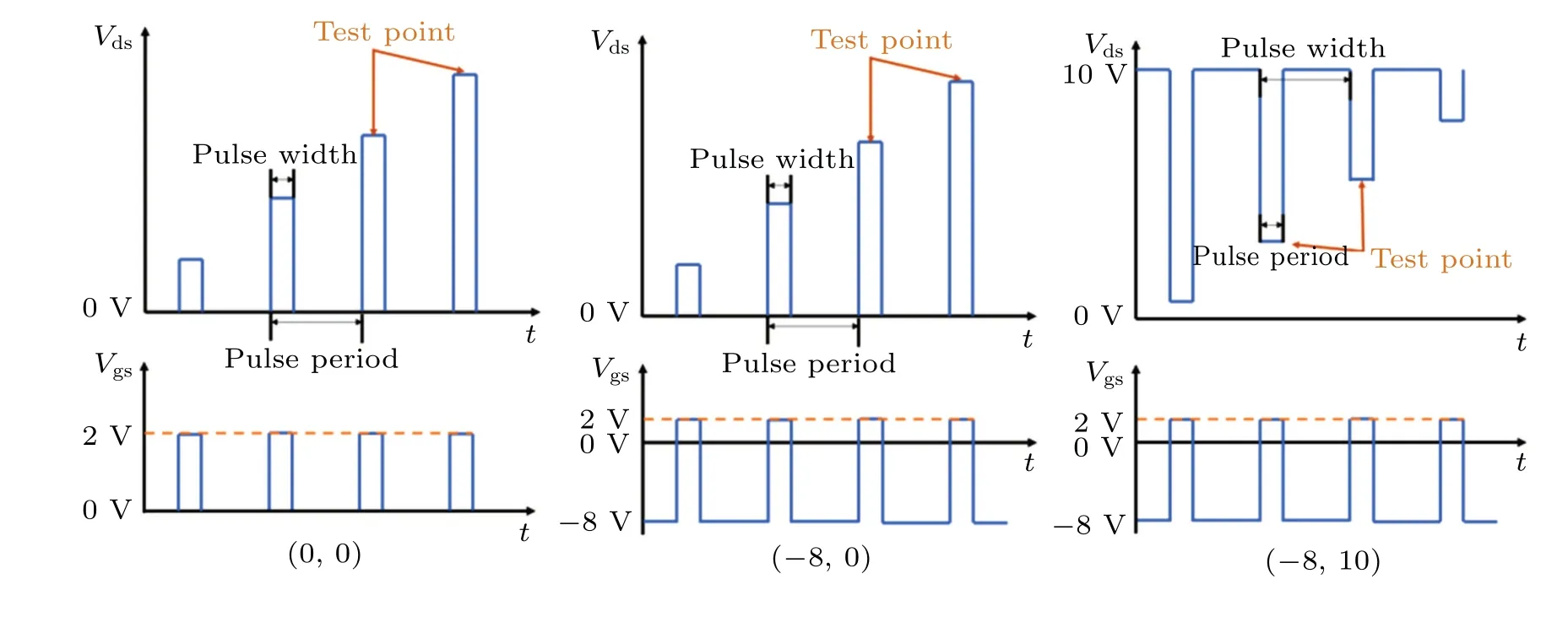
Fig.5. Schematic of pulsed I-V testing.
Figure 6 shows the results of pulsedID-VDtesting with a pulse width of 500 ns atVg=2 V before and after irradiation.At(-8,0)and(-8,10)states,the electrons in the channel were depleted and the device was in the off state. Current collapse at(-8,0)and(-8,10)states is likely due to the electrons trapped under the gate and the gate-drain access region, respectively. Because current collapse did not occur in the(0,0)state, the (0,0) state was taken as the reference state for current collapse. The greater the surface state density, the more electrons that are trapped and the greater the current collapse caused by the surface state.Therefore,the surface state density of the gate and gate-drain region can be indirectly measured by the pulsed test method. To quantitatively study the current collapse, the amount of current collapse is defined according to Eq.(3). The drain current is selected in the deep saturation region(VDS=10 V).[37]

As shown in Fig. 6, the drain currents at (-8,0) and(-8,10)states were lower than that at the(0,0)state,because electrons were injected from the gate to the gate-drain region and were trapped by the surface states, causing current collapse. At the (-8,10) state, the electric field is larger on the drain side of the gate edge, more electrons are injected into the gate-drain region, and more electrons are trapped by the surface state, so the pulse output current is the smallest. The amount of current collapse after irradiation was greater than that before irradiation, especially at the fluence of 1×10¹⁰ions/cm2. This is likely due to the introduction of more surface state traps by irradiation. The higher the surface state density,the higher the quantity of electrons that are trapped and the more serious the current collapse. Augaudyet al.posited that these effects are mainly related to the time constants associated with the electron capture and emission process.[38]
Figure 7 shows the output characteristics of the devices under DC conditions and at different quiescent bias conditions.The pulse width varied from 500 ns to 100 μs, and the pulse period was 1 ms. Before irradiation, the drain current under pulsed testing was higher than that under DC testing. As the pulse width increased, the drain current decreased. The decrease inId-pulseis generally considered due to the captured electrons in the traps, and electron capture by traps may occur when the voltage changes to the test voltage. When the pulse width is 500 ns,there is insufficient time for the surface traps to capture electrons; therefore,the pulse currentId-pulseis much larger than the DC currentId-dc. As the pulse width increases,the surface traps have sufficient time to capture electrons;therefore,the pulse current decreases.
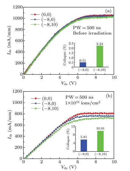
Fig.6. Comparison of different quiescent bias condition with the same pulse width (pulse width (PW) = 500 ns), (a) before irradiation (b)1×10¹⁰ ions/cm2.The current collapse amounts are shown in the insets.

Fig.7. The output characteristics(Vgs=2 V)in different pulsed conditions before and after irradiation,(a)and(b)are for(0,0)state,(c)and(d)are for(-8,0)state,(e)and(f)are for(-8,10)state.

Fig.8. The relationship between Id-pulse/Id-dc and pulse width at different quiescent bias conditions,(a)(0,0)state,(b)(-8,0)state,(c)(-8,10)state.
As shown in Fig. 7, the difference in pulse current between the pulse widths of 10 μs and 100 μs was the smallest after heavy ion irradiation at the fluence of 1×10¹⁰ions/cm2.After heavy ion irradiation,there were few surface states with time constants in the range of 10 μs<τ <100 μs and many surface traps with time constants in the range of 500 ns<τ <10 μs.
We used Eqs.(4)-(6)to fit the variation inId-pulse/Id-dcwith pulse width to obtain the corresponding trap time constant.In these equations,IDCis the DC drain current,whileτ1,τ2andτ3are the trap time constants. Moreover,I1,I2andI3are the fitting constants,[29]
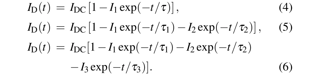
Figure 8 shows the relationship betweenId-pulse/Id-dcand the pulse width at different quiescent bias conditions. The aforementioned equations were used to fit the experimental data. The fitted trap time constants are shown in Fig.9. Equation(6)was used to fit the experimental data obtained before irradiation,while Eq.(4)was used for the data obtained after irradiation. The results revealed that traps with time constants in the range of 10 μs<t <100 μs disappeared after the irradiation.
In summary,more surface state traps are introduced after heavy ion irradiation. Moreover,the time constants of the surface traps induced by heavy ion irradiation are concentrated between 500 ns and 10 μs.

Fig.9. The fitting trap time constant of devices before and after irradiation.
4. Conclusion
In this paper, the evolution of interface traps at the gate/AlGaN layer in AlGaN/GaN HEMTs under 2.1 GeV181Ta32+heavy ion irradiation was investigated in detail.The characteristics of the interface traps were determined by pulsedI-Vtesting. A quantitative comparison of current collapse revealed that irradiation introduced more surface traps.However,by comparing the different pulse widths at the same quiescent operating point,we found that heavy ion irradiation reduced the amount of surface trap states with time constants between 10 μs and 100 μs.Therefore,heavy ion irradiation introduced more trap states with time constants less than 10 μs.The results presented herein facilitate our understanding of the effects of heavy ion irradiation on interface traps in Al-GaN/GaN HEMTs.
Acknowledgements
Project supported by the National Natural Science Foundation of China(Grant Nos.12035019 and 11690042)and Science Challenge Projects(Grant No.TZ2018004).
猜你喜欢
杂志排行

Chinese Physics B的其它文章
- Measurements of the 107Ag neutron capture cross sections with pulse height weighting technique at the CSNS Back-n facility
- Measuring Loschmidt echo via Floquet engineering in superconducting circuits
- Electronic structure and spin-orbit coupling in ternary transition metal chalcogenides Cu2TlX2(X =Se,Te)
- Characterization of the N-polar GaN film grown on C-plane sapphire and misoriented C-plane sapphire substrates by MOCVD
- Review on typical applications and computational optimizations based on semiclassical methods in strong-field physics
- Quantum partial least squares regression algorithm for multiple correlation problem