Reveal the large open-circuit voltage deficit of all-inorganic CsPbIBr2 perovskite solar cells
2022-03-12YingHu胡颖JiapingWang王家平PengZhao赵鹏ZhenhuaLin林珍华SiyuZhang张思玉JieSu苏杰MiaoZhang张苗JinchengZhang张进成JingjingChang常晶晶andYueHao郝跃
Ying Hu(胡颖) Jiaping Wang(王家平) Peng Zhao(赵鹏) Zhenhua Lin(林珍华) Siyu Zhang(张思玉)Jie Su(苏杰) Miao Zhang(张苗) Jincheng Zhang(张进成) Jingjing Chang(常晶晶) and Yue Hao(郝跃)
1State Key Discipline Laboratory of Wide Band Gap Semiconductor Technology,School of Microelectronics,Xidian University,Xi’an 710071,China
2Advanced Interdisciplinary Research Center for Flexible Electronics,Xidian University,Xi’an 710071,China
Keywords: all-inorganic perovskites,CsPbIBr2 solar cells,device simulation,voltage loss,Silvaco TCAD
1. Introduction
Since Miyasakaet al.first employed perovskites as the photovoltaic absorber in 2009,[1]organic-inorganic lead halide perovskites have attracted great attention in photovoltaic applications. In recent years, the power conversion efficiency (PCE) of single-junction cells has been elevated to 25.5% closing to the Shockley-Queisser (S-Q) limit,[2,3]which is attributed to lots of researchers devoting to the exploration of perovskite solar cells(PSCs).[4-8]More importantly,the main reason for the success is that lead halide perovskites possess excellent optical and electrical properties, including tunable bandgap, high light absorption coefficient, low exciton binding energy,long carrier diffusion length,and long carrier lifetime.[5,8-15]However, conventional organic-inorganic hybrid PSCs contain organic cations,such as MA+and FA+,which tend to evaporate and react with water molecules in the air and be easily decomposed by heat.[16-18]Considering superior thermal stability of perovskite material, the all-inorganic perovskites, such as CsPbI3, CsPbI2Br, CsPbIBr2, CsPbBr3,eliminate the organic components, which are the promising wide-bandgap candidates.[19-28]As the all-inorganic CsPbI3PSC was first reported by Snaithet al.with the PCE of 2.9%,[29]researchers have continuously improved the fabrication process of PSCs. In 2020, Sang Il Seok team reported a PCE of 20.37 % for all-inorganic PSCs, through adding a methylammonium chloride solution to accelerate the crystallization process of the all-inorganic perovskite, therefore the highly uniform and pinhole-minimized thin films were obtained,followed by surface passivation using octyl ammonium iodides in ambient air.[30]The highest PCE up to now for allinorganic PSCs is 20.8%,since an environmentally benign material,histamine(HA),is designed to passivate the iodine vacancies in the perovskite thin film.[31]Yanget al.reported dye molecule-assisted engineering as interface passivation, thus reducing the interfacial charge recombination to obtain recordhigh open circuit voltage (Voc) of 1.37 V and minimum voltage loss (Vloss=Eg/q-Voc) of 0.68 V for CsPbIBr2(with a bandgap of 2.05 eV) PSCs, thisVlossis even higher than that of CsPbBr3(with a wider bandgap of 2.3 eV) PSCs.[19]At present, the highest reportedVocof CsPbBr3PSCs is 1.70 V,corresponding to a minimumVlossof 0.60 V.[32]Limited by severeVloss,the current record-high PCE of CsPbIBr2PSCs is 11.04%, which is well below theoretical values of 21%.[33]Therefore, to further optimize the performance, theoretical analysis and research of CsPbIBr2PSCsVlossshould be carried out.
Generally speaking,minimizing the non-radiative recombination loss is vital to improveVocand reduceVloss. Defects passivation of perovskite grain boundaries or film surface has been proved to be an effective measure to suppress the non-radiative recombination.[19,34-38]In addition, the modification of the energy level alignment between perovskite layer and adjacent charge transport layer (CTL) can reduce charge recombination loss and facilitate charge extraction at perovskite/CTL interface.[39]In the following parts,CsPbIBr2PSC is employed to investigate the reasons for the highVloss,and is expected to provide a guideline for designing high performance CsPbIBr2PSC with lowVloss. Firstly, the effect of the absorption layer thickness is studied comprehensively,and the optimal thickness is 200 nm.To achieve better energy level alignment, the influence of conduction and valence band offset is studied, and theVocof CsPbIBr2PSC with ZnO ETL is improved from 1.37 V to 1.52 V compared with SnO2. In addition, the optimum doping concentrations of SnO2electron transport layer(ETL)and Spiro-OMeTAD hole transport layer (HTL) are 1019cm-3and 1021cm-3, respectively. Finally,the minimalVlossand optimal performance are achieved when the cathode electrode work function is between-4.8 eV and-4.6 eV and the anode electrode work function is between-5.4 eV and-5.2 eV.
2. Method
In this study, optoelectronic simulator Silvaco TCAD is employed to optimize PSC. All-inorganic perovskite CsPbIBr2is used as the absorption layer.According to the existing reports, SnO2ETL and Spiro-OMeTAD(2,2′,7,7′-Tetrakis[N,N-di(4-methoxyphenyl)aMino]-9,9′-
spirobifluorene) HTL in the CsPbIBr2PSC have the lowestVloss,[19]therefore, the planar device structure ITO/SnO2/CsPbIBr2/Spiro-OMeTAD/Ag is adopted in this study and shown in Fig. S1. Electrical parameters of the PSC are obtained from the literature and summarized in Table S1.[19,39-42]The theoretical analysis and simulation of PSCs are mainly based on the Poisson equation (Eq. (1)),carrier continuity(Eq.(2)),and drift-diffusion(Eq.(3));[43]
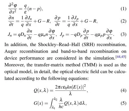
whereε0is the vacuum permittivity,cis the speed of light,nandkare the real and imaginary parts of the refractive index,respectively,|E(x)|2is the optical electric field,his the Planck constant,λis the wavelength,andG(x)is the carrier generation rate. The refractive indexnand extinction coefficientkof all-inorganic perovskites are obtained from the literature.[42,45]This work is simulated under the standard AM1.5G solar spectrum.
3. Results and discussion
3.1. Optimization of perovskite layer thickness
The perovskite absorption layer acts as the most important layer in PSC by absorbing light and converting into excitons or free carriers. Therefore, we first explored the influence of CsPbIBr2absorption layer thickness in this section. Figure 1(a)shows that short-circuit current density(Jsc)sharply increases when CsPbIBr2layer thickness is smaller than 100 nm, after that, the increase slows down and reaches saturation at 200 nm, and the saturation current is around 11.84 mA/cm2. TheVocdecreases with the increase of the CsPbIBr2layer thickness. In addition, figures 1(c) and 1(d)show that the filling factor(FF)of the device almost remains unchanged, and PCE reaches saturation when the absorption layer thickness is 200 nm(Jscis 11.83 mA/cm2;Vocis 1.53 V;FF is 85.19%; PCE is 15.53%). Therefore, in the following section, the solar cell with 200 nm CsPbIBr2layer is used as the standard device.

Fig. 1. Performance parameters of PSC device with different thickness of perovskite: (a)Jsc,(b)Voc,(c)FF,and(d)PCE.
To further investigate the reasons for the trend ofJsc,the net carrier generation rate (the difference between the carrier generation rate and the carrier recombination rate) and external quantum efficiency (EQE) of different absorption layer thicknesses are simulated, as shown in Figs. 2(a) and 2(b),respectively. The net charge carrier generation rate increases with the increasing absorption layer thickness and tends to saturate at 200 nm, which is consistent withJsc. According to the EQE simulation results, with the perovskite layer thickness increasing from 50 nm to 300 nm, the EQE in shortwavelength region (<400 nm) is almost unchanged, on the contrary, the EQE in long-wavelength region (>400 nm) is significantly improved, which indicates that photons in the short-wavelength region(<400 nm)can be almost completely absorbed by the thin perovskite film and the thickness increase mainly induces the improvement of photon absorption in the long-wavelength region (>400 nm). Moreover, the situation of EQE is similar with that ofJsc.

Fig.2. (a)Net carrier generation rate and(b)EQE of PSCs with different thickness of perovskite layer. (c)Carrier generation rate and(d)energy band diagrams of the device with different perovskite layer thickness.
In order to further explore theVocvariation, the carrier generation rate per unit thickness of the absorption layer is shown in Fig. 2(c) and exhibits an obvious declining trend,which indicates that the non-equilibrium carrier concentration reduces with the increase of the CsPbIBr2thickness.As we all know, electron quasi-Fermi level (Efn) and hole quasi-Fermi level (Efp) tend to close to each other due to the reduction of the non-equilibrium carrier concentration, in addition,Vocis proportional to the difference betweenEfnandEfp. Therefore,the difference betweenEfnandEfp(Fig.2(d))decreases with the increase of the perovskite absorption layer thickness,which is the reason thatVockeeps decreasing.
According to Eqs. (4) and (5), the photoelectric field of perovskite layers with different thickness is studied under the condition of 400 nm,480 nm,550 nm and 600 nm wavelengths respectively. Overall,the peak value of the photoelectric field increases with the wavelength from 400 nm to 550 nm, and then decreases at the wavelength of 600 nm.In Fig.3(a),when the wavelength is 400 nm,the curves are almost overlapping,and the smooth descent of these curves indicates that there is no interference in the photoelectric field. Compared with the 400 nm wavelength, an obvious optical interference occurs when the wavelengths are 550 nm and 600 nm, as shown in Figs.3(c)and 3(d).At the same wavelength,although the peak value of the photoelectric field decreases with the increase of the absorption layer thickness, the thicker absorber layer can continuously generate more carriers. These conclusions about the photoelectric field of various wavelengths are consistent with the EQE results in Fig.2(b).

Fig.3. Optical electric field(|E(x)|2)of(a)400 nm wavelength,(b)480 nm wavelength,(c)550 nm wavelength and(d)600 nm wavelength.
3.2. Influence of conduction and valence band offset on device performance with interface defect layer
According to the previous research, the highestVocof the all-inorganic CsPbIBr2PSC is only 1.37 V,[19]which is far lower than the 1.53 V obtained by the standard device in this study. The highVlossof the wide bandgap perovskite attributes to interface defects and band offset. Therefore, in this section, the influences of conduction band offset (CBO)and valence band offset(VBO)are studied. According to the literature,[46]we define 10 nm interface defect layer 1(IDL1)and 2(IDL2)at each of the interfaces of perovskite/ETL and perovskite/HTL,respectively.
3.2.1. Conduction band offset of perovskite/ETL layer

In Fig.4(a),theJ-Vcurves are almost overlapping when CBO increases from 0 to 0.5 eV, after that, when CBO exceeds 0.6 eV,Jscand FF drop sharply.Vocincreases significantly when CBO increases from-0.6 eV to 0 eV.As shown in Fig. 4(b), there is a spike at the IDL1/ETL interface, and the barrier increases significantly when CBO exceeds 0.5 eV.Carrier transport from absorption layer to ETL is obviously impeded, resulting in the decline ofJscand FF. As forVoc,when CBO is-0.5 eV (Fig. 4(c)), the energy band diagram of PSCs shows that there is a cliff at the IDL1/perovskite interface. The cliff does not impede the electron transfer from perovskite to IDL1,however it leads to the increase of the carrier recombination rate in IDL1. In Fig.4(d), the recombination rate reduces with the decrease of|CBO|. In addition,the spike impedes both photogeneration current (IL) and the forward current(IS),which leads to the decline of bothILandIS(Eq. (6)), therefore theVocremains constant at a fixed value when CBO is positive. In summary, when CBO is 0-0.5 eV,the optimal PCE(16.78%)of the device could be obtained.

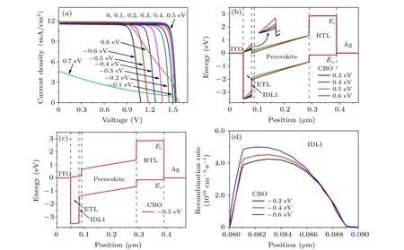
Fig. 4. (a) The J-V curves of the PSCs with different CBOs. (b) Energy band diagrams with the positive value of CBOs, and (c) energy band diagram with the negative value(-0.5 eV)of CBO.(d)Recombination rate in IDL1 of the device with different CBO.

Fig.5. (a)Energy band positions of the device. (b)The J-V curves,(c)energy band diagrams,(d)internal longitudinal electric field of the device with different CBO of PSCs with SnO2 and ZnO as ETL,respectively.

Fig.6. (a)The J-V curves of the PSCs with different VBOs.(b)Energy band diagrams,and(c)recombination rate in IDL2 with the negative valuesof VBOs. (d)Energy band diagrams with the positive values of VBOs.
TheVocof the PSCs with SnO2ETL is only 1.37 V. The Csbased PSCs with ZnO ETLs have been widely studied, and have achieved competitive efficiency and stability over those with other metal oxides in our previous study.[47]In order to obtain better device performance, ZnO ETL is investigated to suppressVlossin PSCs. The material parameters of ZnO are obtained from the literature,[48]and the band diagram is shown in Fig. 5(a), it can be found that the conduction band of ZnO(CBO is-0.05 eV)is more suitable than that of SnO2(CBO is-0.3 eV).According to the result of theJ-Vcurves in Fig.5(b),the device performance with ZnO ETL is superior to that with SnO2ETL.Jscincreases from 11.58 mA/cm2to 11.97 mA/cm2, which attributes to the smaller parasitic absorption induced by the wider bandgap of ZnO. In addition,Voc(FF) increases from 1.37 V (84.92%) to 1.52 V (87.91%). This is because there is no cliff based on ZnO ETL compared with SnO2ETL, as shown in Fig. 5(c), resulting in lower carrier recombination rate.Moreover,as shown in Fig.5(d),the internal electric field with ZnO ETL is about 1 V/μm larger than that with SnO2ETL, which is conducive to the collection and extracting of carriers. Finally,the PCE of ZnO-based PSC(15.90%)is better than that of SnO2-based PSC(13.47%). Consequently,the conduction band of ETL material should be more matching with that of perovskite in order to eliminateVlossinduced by CBO as much as possible.
3.2.2. Valence band offset of perovskite/HTL layer
As shown in Fig. S3(a), whenEvHTLis greater thanEvperovskite, VBO is set to be negative, andEvIDL2(EcIDL2)is set to be consistent withEvHTL(Ecperovskite). In Fig.S3(b),whenEvperovskiteis greater thanEvHTL,VBO is set to be positive,andEcIDL2andEvIDL2are set to be consistent with perovskite. The charge carrier lifetime of IDL2 is set to be 1 ns,other optical and electrical parameters are identical to the perovskite layer.
As shown in Fig. 6(a),Vocdecreases obviously with the VBO declining from 0 to-0.5 eV.Jscalmost remains constant and FF decreases slightly. As shown in Fig.6(b), when the VBO is negative,the cliff at the IDL2/perovskite interface rises with the raise of|VBO|,which leads to the increase of the carrier recombination rate in IDL2 (Fig. 6(c)). This explains the variation of performance parameters in Fig.6(a). In addition,the device performance drops significantly when VBO is larger than 0.3 eV. A spike is formed at the IDL2/HTL interface (Fig. 6(d)), and the barrier increases significantly when VBO exceeds 0.3 eV. Carrier transport from absorption layer to HTL is seriously impeded,resulting in the decline ofJscand FF.In addition,Vocis almost constant when VBO is positive,and the reason is consistent with the analysis in the previous section. In summary,when VBO is 0-0.3 eV,the optimal PCE(16.09%)and minimumVlossof the device could be obtained.
3.3. Optimization of doping concentration of charge transport layer
According to the previous reports, the doping of ETL could affect the extraction of free carriers and the device performance. The doping concentration of the ETL and HTL layer could be controlled by ion doping engineering approaches in experiments. In the simulation, doping concentrations of both ETL and HTL can be achieved by controlling the dopants type (donor concentration and acceptor concentration). The n-type doping concentration of the ETL layer is controlled and varied from 1015cm-3to 1021cm-3to study its influence on the performance in this work. As shown in Fig.7,Jscdecreases slightly with the increase of SnO2doping concentration. TheVocand FF increase firstly and then tend to saturate. The EQE almost remains constant with various ETL doping concentration (Fig. 8(a)), which indicates that the influence of the ETL doping concentration on light absorption is negligible.
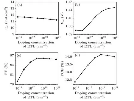
Fig.7.Performance parameters of PSCs with different doping concentration of ETL:(a)Jsc,(b)Voc,(c)FF,and(d)PCE.

Fig.8. (a)EQE,(b)recombination rate,(c)energy band diagrams,(d)internal longitudinal electric field with different doping concentration of ETL.
Figure 8(b) shows the carrier recombination rate in the SnO2layer. Impurity is a kind of recombination center,therefore the increase of doping concentration induces the reduction of carrier mobility,resulting in the increase of non-radiative recombination in ETL,leading to the decrease ofJsc. As shown in Fig. 8(c), the cliff does not change between the perovskite layer and IDL1 with the increase of SnO2doping concentration, therefore, the interface defect recombination rate is almost unchanged, however, the built-in electric fields in IDL1 and ETL significantly increase (Fig. 8(d)), so that the carriers can be collected more efficiently,this is consistent with the change ofVocand FF.Finally,the optimal efficiency is 14.15%when the SnO2doping concentration is 1019cm3.
In addition,the different doping concentrations of Spiro-OMeTAD could affectVocand performance of PSCs as well.The p-type doping concentration of the HTL layer is varied from 1015cm-3to 1021cm-3. Figure 9(a) shows thatJscdecreases slightly with the increase of the Spiro-OMeTAD doping concentration, the main reason is that a large number of metal ions are added to produce the recombination center,which makes the non-radiative recombination in HTL increase sharply as shown in Fig.10(a),leading to the decrease ofJsc.Moreover, figure 9(b) shows thatVocincreases significantly with the increase of the Spiro-OMeTAD doping concentration. The reason is, on the one hand, the energy band position is pulled higher with the increase of the Spiro-OMeTAD doping concentration (Fig. 10(b)), leading to the increase of the electric field in the interface defect layer IDL2, as shown in Fig. 10(c), so the carrier is extracted and separated efficiently by HTL. On the other hand, the cliff is unchanged,which results in that the interface defect recombination does not increase. Consequently,when the doping concentration of Spiro-OMeTAD is 1021cm-3,Vocis improved from 1.14 V to 1.23 V effectively,and the optimal PCE is 12.04%.

Fig.9.Performance parameters of PSCs with different doping concentration of HTL:(a)Jsc,(b)Voc,(c)FF,and(d)PCE.

Fig.10. (a)Recombination rate,(b)energy band diagrams(c)internal longitudinal electric field with different doping concentration of HTL.
3.4. Influence of electrode work function
In the above study,cathode and anode electrodes are set to ohmic contact. However,the Schottky contact between carrier transport layer and electrode could not be avoided, resulting in the change of the energy band diagrams. Thus,it is meaningful to explore the effect of cathode electrode work function(Φcathode) and anode electrode work function (Φanode) on the performance of PSCs.
3.4.1. Influence of cathode electrode work function
In order to avoid the influence ofΦanode, the contact between HTL and anode electrode is set to ohmic contact.By comparingJ-Vcurves corresponding to differentΦcathodefrom-4.8 eV to-6.2 eV (Fig. 11(a)), the device performance decreases significantly. As shown in Fig. 11(b), the conduction band of SnO2keeps elevating with the decrease ofΦcathodefrom-4.8 eV to-6.2 eV, the slope of the energy band of the perovskite layer drastically reduces, which results in a significant decrease of the built-in electric field in the device, leading to the inefficient extraction of free carriers in the perovskite layer (Fig. 11(c)). Furthermore, a spike is formed in the energy band whenΦcathodeis between-5.4 eV and-6.2 eV, therefore, the negative electric field is generated inside the perovskite layer. This situation seriously hinders the transport of the carrier and results in the loss of the device performance. According to Figs.11(d)and 11(e),the carrier concentration increases with the decrease ofΦcathodefrom-4.8 eV to-5.4 eV, however, whenΦcathodeis between-5.8 eV and-6.2 eV, a large number of charge carriers cannot be efficiently collected by the corresponding charge transfer layer, resulting in the accumulation of carriers, which will lead to the increase of interface recombination and the loss ofVoc. In summary,the optimal performance of PSC (Jsc=11.86 mA/cm2,Voc=1.54 V, FF=82.87%,PCE = 15.13%) can be obtained whenΦcathodeis between-4.8 eV and-4.6 eV. Generally speaking, transparent conductive oxide(TCO)film is used as cathode electrode in planar forward structure PSCs,Hence,ITO and FTO are suitable for the device structure in this study.
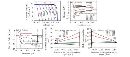
Fig.11. (a)The J-V curves,(b)energy band diagrams and(c)internal longitudinal electric field of PSCs with different Φcathode. (d)Electron and(e)hole concentration distributions of the perovskite layer with various Φcathode.
3.4.2. Influence of anode electrode work function
In this section, the contact between ETL and cathode electrode is set to ohmic contact. As shown in Fig. 12(a),the performance increases significantly with the decrease ofΦanodefrom-4.0 eV to-5.4 eV.For planar forward structure PSCs,the anode electrode is usually made of metal. When the metal electrode is Schottky contact with the p-type semiconductor,

Fig.12. (a)The J-V curves,(b)energy band diagrams and(c)internal longitudinal electric field of PSCs with different Φanode. (d)Electron and(e)hole concentration distributions of the perovskite layer with various Φanode.
4. Conclusion
Several factors that affect theVocand the performance of single-junction CsPbIBr2PSC are investigated. Firstly, the thickness of the absorption layer is studied and the optimal value is 200 nm. As for CBO, when the conduction band of perovskite is higher than that of ETL, the band cliff leads to the increase of the carrier recombination rate in the interface defect layer, andVlossincreases obviously. In contrast,when the conduction band of perovskite is lower than that of ETL, the spike seriously hinders the transport of carriers from the absorber layer to ETL, resulting in the decrease ofJscand FF, however, there is almost no influence onVocdue to the decrease of both the photoelectric current and the forward current. The suitable value of CBO is 0-0.5 eV,and theVocof CsPbIBr2PSC with ZnO ETL increases significantly from 1.37 V to 1.52 V compared with that with SnO2ETL,owing to the better matching conduction band with CsPbIBr2absorption layer. The optimum VBO is 0-0.3 eV,and the reason is similar to CBO. What’s more, the doping concentration of CTL is optimized to minimizeVlossand improve the performance. The optimum doping concentrations of SnO2and Spiro-OMeTAD are 1019cm-3and 1021cm-3, respectively. Finally,whenΦcathode(Φanode)is between-4.8 eV and-4.6 eV (between-5.4 eV and-5.2 eV), the minimalVlossand optimal performance are obtained.
Acknowledgements
This work was financially supported by the National Natural Science Foundation of China (Grant No. 52192610),the Key Research and Development Program of Shaanxi Province, China (Grant No. 2020GY-310), Youth Project of Natural Science Basic Research Program of Shaanxi Province, China (Grant No. 2021JQ-189), the Joint Research Funds of Department of Science & Technology of Shaanxi Province and Northwestern Polytechnical University(Grant No.2020GXLH-Z-018),and the Fundamental Research Funds for the Central Universities,China.
猜你喜欢
杂志排行
Chinese Physics B的其它文章
- Measurements of the 107Ag neutron capture cross sections with pulse height weighting technique at the CSNS Back-n facility
- Measuring Loschmidt echo via Floquet engineering in superconducting circuits
- Electronic structure and spin-orbit coupling in ternary transition metal chalcogenides Cu2TlX2(X =Se,Te)
- Characterization of the N-polar GaN film grown on C-plane sapphire and misoriented C-plane sapphire substrates by MOCVD
- Review on typical applications and computational optimizations based on semiclassical methods in strong-field physics
- Quantum partial least squares regression algorithm for multiple correlation problem
