High power-added-efficiency AlGaN/GaN HEMTs fabricated by atomic level controlled etching
2022-02-24XinchuangZhang张新创BinHou侯斌FuchunJia贾富春HaoLu芦浩XueruiNiu牛雪锐MeiWu武玫MengZhang张濛JialeDu杜佳乐LingYang杨凌XiaohuaMa马晓华andYueHao郝跃
Xinchuang Zhang(张新创) Bin Hou(侯斌) Fuchun Jia(贾富春) Hao Lu(芦浩)Xuerui Niu(牛雪锐) Mei Wu(武玫) Meng Zhang(张濛) Jiale Du(杜佳乐)Ling Yang(杨凌) Xiaohua Ma(马晓华) and Yue Hao(郝跃)
1School of Advanced Materials and Nanotechnology,Xidian University,Xi’an 710071,China2School of Microelectronics,Xidian University,Xi’an 710071,China
An atomic-level controlled etching(ACE)technology is invstigated for the fabrication of recessed gate AlGaN/GaN high-electron-mobility transistors(HEMTs)with high power added efficiency. We compare the recessed gate HEMTs with conventional etching(CE)based chlorine,Cl2-only ACE and BCl3/Cl2 ACE,respectively. The mixed radicals of BCl3/Cl2 were used as the active reactants in the step of chemical modification. For ensuring precise and controllable etching depth and low etching damage,the kinetic energy of argon ions was accurately controlled. These argon ions were used precisely to remove the chemical modified surface atomic layer. Compared to the HEMTs with CE, the characteristics of devices fabricated by ACE are significantly improved,which benefits from significant reduction of etching damage. For BCl3/Cl2 ACE recessed HEMTs,the load pull test at 17 GHz shows a high power added efficiency(PAE)of 59.8%with an output power density of 1.6 W/mm at Vd=10 V,and a peak PAE of 44.8%with an output power density of 3.2 W/mm at Vd=20 V in a continuous-wave mode.
Keywords: AlGaN/GaN HEMTs,recess etching,low damage,high power added efficiency
1. Introduction
As an excellent representative of third-generation semiconductors,GaN HEMT heterojunction is widely used in high frequency, high efficiency and high power fields, attributing to its high electron mobility (~2000 cm2/V·s), high density(1013cm−2) and high critical breakdown electric field.[1–5]The fabrication of a large number of GaN power electronic devices and RF power devices strongly depends on the etching process.[6–9]However, conventional etching (CE) based on plasma, such as reactive ion etching (RIE) and inductively coupled plasma (ICP), often suffers from some prickly problems including large significant etching damage and uncontrollable etching depth.[10,11]To solve the above problem,atomic layer etching(ALE)of GaN based on XeF2/BCl3and Cl2/Ar has been proposed.[12,13]Nevertheless, Ohbaet al.found that an ultrasmooth surface could be realized by ALE based on BCl3/Cl2, while ALE based on chlorine-only could result in a rough surface morphology.[14]Kimet al.found that when BCl3is added to Cl2, the density of Cl+andcould be significantly reduced during the gas was glow. The decrease of Cl+anddensity can significantly reduce the plasma damage.[15]This shows that ALE based on BCl3/Cl2is more potential than ALE of chlorine-only. However, Ohbaet al.only studied the etching process of AlGaN.[14]Reports on GaN radio frequency devices fabricated by BCl3/Cl2based ALE are still lacking.
In this work,we developed a BCl3/Cl2and Cl2-only based atomic level controlled etching(ACE)technology for AlGaN.By BCl3/Cl2and Cl2-only based ACE technology, we fabricated recessed gate HEMTs devices and compared them with HEMTs fabricated by CE process. For the recessed HEMTs with Cl2-only ACE and BCl3/Cl2ACE technology,theIon/Ioffratios of the device are increased by one order of magnitude and more than two orders of magnitude, respectively. At the same time, the DC peak transconductance is increased from 375 mS/mm to 453 mS/mm and 540 mS/mm. At 17 GHz,the HEMTs with Cl2-only ACE and BCl3/Cl2ACE,respectively,exhibit attractive peak power added efficiency(PAE)of 57.1%and 59.8% at drain bias of 10 V in a continuous-wave mode.The results presented here are believed to boost the low damage etching process for radio frequency applications.
2. Process mechanism of ACE technology
As shown in Fig. 1, the basic BCl3/Cl2ACE concept consists of chemical modification and physical removal.BCl3/Cl2-based chemistry is used in ACE for GaN.BCl3/Cl2-based free radicals remove residual oxygen and chemically modify the surface atoms of AlGaN, which improve chlorination coverage.[16–18]In the physical reaction step, the kinetic energy of argon ion is precisely controlled by a pulse-time-regulated RF power,sequentially the chlorine atom layer is just removed.[19–21]A chlorinated layer is formed by the self-limiting chemical reaction between an atomic layer on the GaN surface and the mixed radicals of BCl3/Cl2in Fig.1(step 1), ionized by an ICP coil power with the radio frequency of 13.56 MHz. After purging the surplus radicals,the chlorinated layer is removed by argon ions in Fig. 2 (step 2),followed by purging of by-products with BCl3/Cl2. The detailed process parameters are shown in the arrow flow charts.It should be noted that the pulse duty in Fig.2(step 2)is 30%.
As shown in Fig. 2(a), the AFM (atomic force microscope) scanning morphologies of the etched area surface of the AlGaN samples with 20, 50, 100, 150 and 200 etching cycles are shown with the surface roughness of 0.221 0.241 0.257 0.259 and 0.313 nm by BCl3/Cl2ACE, and the corresponding etching depths are 11, 26, 52, 78 and 105 nm, respectively. The root-mean-square(RMS)roughness of initial un-etching sample is 0.253 nm. With the increase of the number of ACE cycles, the etching depth increases linearly, and the surface roughness of the etched area remains constant at a very low level. The etch per cycle (EPC) is 0.52 nm/cycle,which is in agreement with the lattice constant of GaN alongcaxis.[22]Although the numbers of ACE cycles for all the samples are different, their EPCs are the same, which indicates that the ACE technology has excellent repeatability and stability. What’s more, BCl3/Cl2ACE is capable of realizing atomic-scale control of AlGaN. The EPC of Cl2-only ACE is 0.54 nm/cycle which is slightly larger than the ones of BCl3/Cl2ACE.This may be due to the plasma damage caused by more Cl+andin the chlorine plasma. By adding BCl3into Cl2, the concentration of Cl+andis reduced and the plasma damage is suppressed in the step of chemical modification.[15]Figure 2(b) compares between chemical modification only, physical removal only, and the EPC of BCl3/Cl2ACE(full cycle). The two key steps(in Fig.1 step 1 and step 2)are executed separately for 200 cycles.The EPC of chemical modification is zero,while ones of physical removal is 0.07 nm/cycle. This indicates that the chemical modification and physical removal of BCl3/Cl2ACE are completely separated in time. However, the EPC of chemical modification only and the ones of physical removal only for Cl2-only ACE are 0.02 and 0.07 nm/cycle. This result shows that there is a slight etching effect in the chlorine glow process.

Fig.1. ACE cyclic process: (a)chlorination of GaN surface atomic layer by BCl3/Cl2 radicals; (b)pump out the excessive free radicals and purge chamber with Ar; (c)argon ion bombards the chlorinated atomic layer to form; (d)pump out the by-products and purge chamber with BCl3/Cl2.

Fig.2. (a)Etching depth and RMS roughness versus the number of BCl3/Cl2 ACE cycles(inset: surface topography(area: 5µm×5µm)of the initial unetched sample and the sample with 200 cycles ACE).(b)Result of EPC test based on BCl3/Cl2.
3. Device structure and fabrication
As shown in Fig. 3(a), the AlGaN/GaN HEMT fabricated in this work was grown on a 3-inch SiC substrate,which comprises a 3-nm GaN cap layer, a 21-nm Al0.25Ga0.75N barrier layer, a 400-nm i-GaN channel, and a GaN buffer layer from top to bottom. An electron sheet concentration of 8.29×1012cm−2,a sheet resistance of 303 Ω/□,and a mobility of 1946 cm2/V·s were measured by room-temperature Hall measurements. The ohmic contact formation of source and drain included a deposition of Ti/Al/Ni/Au metal stack and annealed at 840°C for 30 s in N2. Nitrogen ion implantation was then used for device isolation. Transfer length method(TLM)showed an ohmic contact resistance of 0.39 Ω·mm. A 60-nm plasma enhanced chemical vapor deposition(PECVD)SiNxwas utilized as a passivation layer. Electron beam lithography defined the recessed-gate foot of 0.17 µm. After CF4based plasma removing the passivation layer,the AlGaN barrier layer was recessed by BCl3/Cl2ACE and Cl2-only ACE technology. The recessed depth was measured to be 18 nm by AFM with 35 and 33 cycles, resulting in an EPC of 0.52 and 0.54 nm/cycle, respectively. For comparison, 18 nm recess was etched by CE process (the rate of CE is 3 nm/min with an ICP coil power of 150 W,a bias power of 5 W,operating pressure of 5 mTorr,BCl3/Cl2(20 sccm/20 sccm),process time of 6 min),the depth of which was controlled by the process time. Figures 3(b),3(c)and 3(d)illustrate the AFM surface morphology of the sample with CE, Cl2-only ACE and BCl3/Cl2based ACE recessed etching process,respectively. It is shown that the surface morphology maintains a clear and continuous atomic step and a very low surface roughness with RMS roughness of 0.220 nm after BCl3/Cl2based ACE.The Cl2-only ACE-HEMT shows a rough surface morphology with RMS roughness of 0.257 nm,while the recessed gate with CE shows a roughness of 0.353 nm.After the gate lithography,the Ni/Au/Ni gate metal was deposited. The gate root width(Lg),gate head width, source-drain spacing (Lsd), and source-gate space (Lsg) are 0.17 µm, 0.9 µm, 2.5 µm, and 1 µm, respectively.

Fig.3. (a)Schematic diagram of recessed AlGaN/GaN HEMTs, and surface topography(area: 5µm×5µm)of(b)CE recess, (c)Cl2-only ACE recess,and(d)BCl3/Cl2 ACE recess.
4. Results and discussion
The DC transferId–Vg, outputId–Vd, gate reverse Schottky characteristics and the field-effect mobility(µFE)with gate voltage of the recessed gate HEMTs by the CE, Cl2-only ACE and BCl3/Cl2ACE process are performed. As shown in Fig. 4(a), owing to precise controlling bombardment and effectively suppressed etching damage of the ACE technology, the drain leakage current of the device decreases from 2.7×10⁻⁵to 3.7×10⁻⁶and 2.6×10⁻⁷A/mm,theIon/Ioffratio increases from 4.9×10⁴to 4.8×10⁵and 6.8×10⁶,and the peak transconductance of the device increased from 375 to 453 and 540 mS/mm. Figure 4(b)shows that the drain saturation current was raised from 785 to 995 and 1031 mA/mm for three types of HEMTs. As can be seen from Fig. 4(c), compared with the HEMTs by the CE, the gate leakage of HEMTs by Cl2-only ACE and HEMTs by BCl3/Cl2ACE decreases by one order of magnitude and more than two orders of magnitude respectively. Figure 4(d)shows the transferI–Vsweep in linear region and extractedµFEas a function ofVg. TheµFEof the recessed-HEMTs channel was studied withLsg,Lg,LgdandLsdof 3,50,3 and 56µm devices,in which the influence of series resistance on Gm was negligible. The peak mobility of recessed HEMT with the Cl2-only ACE and BCl3/Cl2ACE process is 1204 and 1487 cm2/V·s. However, ones of the HEMT with CE is 953 cm2/V·s. It was probably due to the fact that ACE did not cause the loss of nitrogen in the process of recessing the AlGaN barrier and ultimately reduced the surface trap concentration.[23]The peak mobility of recessed HEMT with the Cl2-only ACE is lower than that of recessed HEMT with BCl3/Cl2ACE, which may be caused by plasma damage during chlorination(Fig.1,step 1).
Figure 5 shows the pulse transfer characteristics of three types of HEMTs at a gate voltage of−6 V to 2 V and the current collapse ratio can be expressed as

where ΔIdsis the variation of drain pulse current (Vg=2 V)before and after electrical stress, andIds0is the drain pulse current(Vg=2 V)before applying electric stress.
The HEMTs with Cl2-only ACE and BCl3/Cl2ACE show current collapse (collapse ratio: 4.1%, Fig. 5(b); 2.7%,Fig. 5(c)), under a quiescent bias of (VGSQ,VDSQ)=(−8 V,0 V). They are all smaller than a value of 6.3% for CEHEMTs.At(VGSQ,VDSQ)=(−8 V,20 V),the current collapse ratio decreases from 25.2% (CE HEMT) to 13.1% (Cl2-only ACE)and 8.5%(BCl3/Cl2ACE).The BCl3/Cl2ACE HEMT and Cl2-only ACE HEMT show tiny threshold voltage shift(ΔVth=0.04 V and 0.14 V) under a quiescent bias of (VGSQ,VDSQ)=(−8 V,20 V),while that of CE ones is 0.28 V.Such shift may be caused by the trapped electrons introduced under the gate during the recessing process.[23]
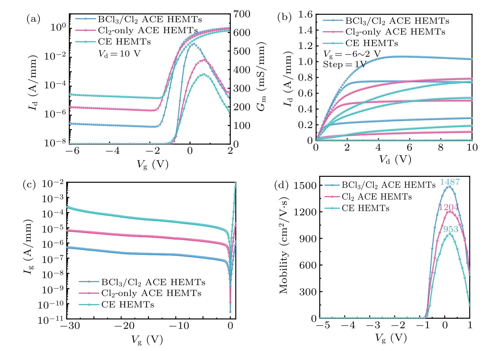
Fig. 4. DC characteristics of the recessed AlGaN/GaN HEMTs with ACE and CE gate recess. (a) Transfer characteristics at Vd =10 V, (b)output characteristics,(c)gate reverse leakage characteristics,(d)field-effect mobility as a function of gate voltage for three types of HEMTs.
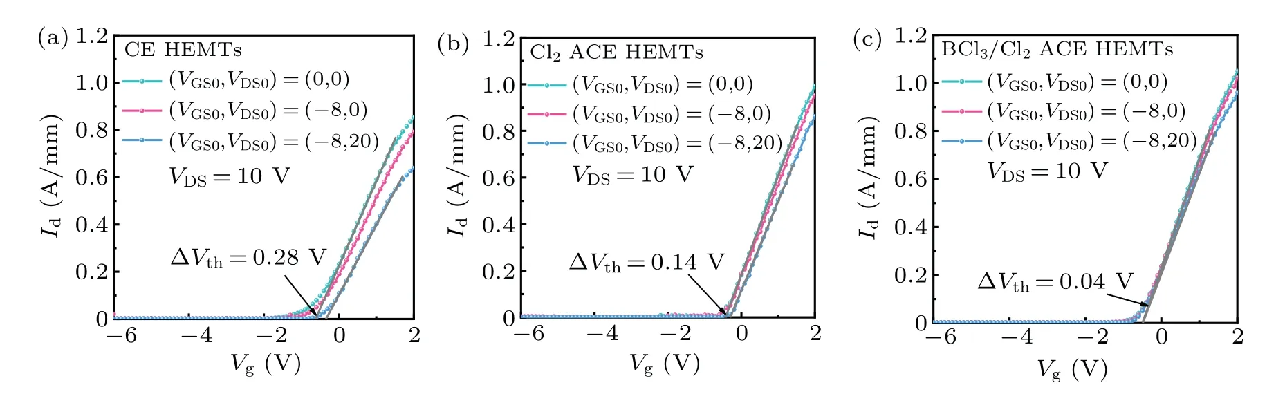
Fig. 5. Pulsed transfer I–V characteristics of recessed gate HEMTs with (a) CE, (b) Cl2-only ACE , (c) BCl3/Cl2 ACE at a gate voltage of−6 V to 2 V for(VGSQ,VDSQ=0 V,0 V),(VGSQ,VDSQ=−8 V,0 V)and(VGSQ,VDSQ=−8 V,20 V).

Fig.6. Small-signal characteristics of the recessed HEMTs at Vd=10 V,Vg=0.2 V with(a)CE gate recess and(b)Cl2-only ACE gate recess,(c)BCl3/Cl2 ACE gate recess.

Fig.7. Load-pull characteristics of the fabricated HEMTs at 17 GHz with WG=2×50µm in CW mode. (a)CE recessed,(b)Cl2-only ACE recessed,and(c)BCl3/Cl2 ACE recessed.
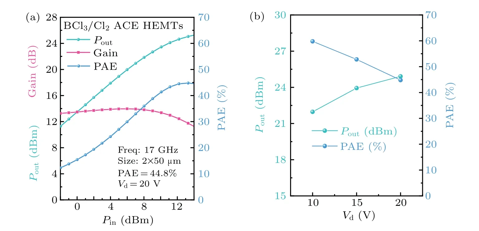
Fig.8. Large-signal characteristics of BCl3/Cl2 ACE HEMTs at 17 GHz with WG=2×50µm in CW mode: (a)at Vd=20 V,(b)RF output power density and peak PAE versus Vd.
Small-signal measurements was used to compare the current-gain cutoff frequency (fT) and maximum oscillation frequency (fmax) of the three kinds of recessed gate HEMTs in the frequency range from 0.1 GHz to 40 GHz. As shown in Figs.6(b)and 6(c),under the same bias condition ofVd=10 V andVg=0.2 V,the BCl3/Cl2ACE-HEMT and Cl2-only ACEHEMT show afT/fmaxof 82/193 GHz and 63/165 GHz, respectively. However, the ones of CE-HEMT were 54 and 138 GHz, respectively, as shown in Fig. 6(a). This is consistent with the law of channel field effect mobility.
The large-signal microwave power measurements of recessed HEMTs with ACE and CE were carried out at 17 GHz in continuous-wave (CW) mode, as shown in Fig. 7. All devices were biased atVd=10 V and class-AB condition. Benefiting from the suppressed gate leakage current as well as the current collapse,[24]the large-signal performance of the recessed HEMTs with ACE has been significantly improved compared with the CE-HEMT,high PAEs of 59.8%and 57.1%are achieved in the BCl3/Cl2ACE-HEMT and Cl2-only ACEHEMT,which is about 10.2%and 7.5%higher than those with CE. In addition, the corresponding output power density has also been increased to 1.6 W/mm and 1.4 W/mm,respectively,while that for the CE HEMTs is 1.0 W/mm.
In order to evaluate the higher voltage operation of the BCl3/Cl2ACE-HEMTs,we performed the large-signal test atVd=20 V biased in a CW mode, as shown in Fig. 8(a). The peak PAE of BCl3/Cl2ACE-HEMTs is 44.8%with the output power density of 3.2 W/mm at 17 GHz. Output power density and peak PAE as a function of drain voltage(Vd=10,15 and 20 V)for BCl3/Cl2ACE-HEMTs are shown in Fig.8(b).WhenVd=15 V, the output power density is 2.5 W/mm and the peak PAE is 52.8%.With the increase of drain bias voltage,the peak PAE decreases,which may be related to the increase of gate leakage current as shown in Fig. 4(c).[25]The further study will focus on the PAE improvement at higher operation voltage such as using N2O plasma treatment.[26]
5. Conclusion and perspectives
An atomic level controlled etching technology is proposed for fabrication of recessed gate AlGaN/GaN HEMTs.Adding BCl3to the chlorination process significantly reduces the roughness of the AlGaN etched surface. The etching depth of the AlGaN can be controlled accurately due to precise power control. The BCl3/Cl2ACE-recessed AlGaN/GaN HEMTs exhibits an attractive PAE of 59.8% at 17 GHz in a CW mode. The ACE technology can solve the current prob-lem of conventional plasma etching in the fabrication of recessed AlGaN/GaN devices, and AlGaN/GaN Fin-FET devices, which is full of potential in the future development of GaN technology.
Acknowledgements
This work was supported by the National Natural Science Foundation of China (Grant Nos. 62090014, 62188102,62104184, 62104178, and 62104179) and the Fundamental Research Funds for the Central Universities of China (Grant Nos.XJS201102,XJS211101,XJS211106,and ZDRC2002).
猜你喜欢
杂志排行

Chinese Physics B的其它文章
- High sensitivity plasmonic temperature sensor based on a side-polished photonic crystal fiber
- Digital synthesis of programmable photonic integrated circuits
- Non-Rayleigh photon statistics of superbunching pseudothermal light
- Refractive index sensing of double Fano resonance excited by nano-cube array coupled with multilayer all-dielectric film
- A novel polarization converter based on the band-stop frequency selective surface
- Effects of pulse energy ratios on plasma characteristics of dual-pulse fiber-optic laser-induced breakdown spectroscopy