A broadband self-powered UV photodetector of a β-Ga2O3/γ-CuI p-n junction
2022-02-24WeiMingSun孙伟铭BingYangSun孙兵阳ShanLi李山GuoLiangMa麻国梁AngGao高昂WeiYuJiang江为宇MaoLinZhang张茂林PeiGangLi李培刚ZengLiu刘增andWeiHuaTang唐为华
Wei-Ming Sun(孙伟铭), Bing-Yang Sun(孙兵阳), Shan Li(李山), Guo-Liang Ma(麻国梁),Ang Gao(高昂), Wei-Yu Jiang(江为宇), Mao-Lin Zhang(张茂林),Pei-Gang Li(李培刚), Zeng Liu(刘增),†, and Wei-Hua Tang(唐为华),,‡
1Laboratory of Information Functional Materials and Devices,School of Science,Beijing University of Posts and Telecommunications,Beijing 100876,China
2College of Integrated Circuit Science and Engineering,Nanjing University of Posts and Telecommunications,Nanjing 210023,China
3National and Local Joint Engineering Laboratory for RF Integration and Micro-Packing Technologies,Nanjing University of Posts and Telecommunications,Nanjing 210023,China
The symmetric Ti/Au bi-layer point electrodes have been successfully patterned on the β-Ga2O3 films which are prepared by metal–organic chemical vapor deposition(MOCVD)and the γ-CuI films which are prepared by spin-coating.The fabricated heterojunction has a large open circuit voltage(Voc)of 0.69 V,desired for achieving self-powered operation of a photodetector.Irradiated by 254-nm ultraviolet (UV) light, when the bias voltage is −5 V, the dark current (Idark)of the device is 0.47 pA,the photocurrent(Iphoto)is −50.93 nA,and the photo-to-dark current ratio(Iphoto/Idark)reaches about 1.08×10⁵.The device has a stable and fast response speed in different wavelengths, the rise time (τr) and decay time(τd)are 0.762 s and 1.741 s under 254-nm UV light illumination,respectively.While the τr and τd are 10.709 s and 7.241 s under 365-nm UV light illumination,respectively.The time-dependent(I–t)response(photocurrent in the order of 10−10 A)can be clearly distinguished at a small light intensity of 1µW·cm−2.The internal physical mechanism affecting the device performances is discussed by the band diagram and charge carrier transfer theory.
Keywords: β-Ga2O3,γ-CuI,heterojunction,broadband photodetector,self-power
1.Introduction
UV light can be divided into four regions according to different wavelengths, short-wave UV light referred to as UVC,wavelength of 200 nm–280 nm,medium-wave ultraviolet light referred to as UVB,wavelength of 280 nm–320 nm,long-wave ultraviolet light referred to as UVA, wavelength of 320 nm–400 nm, UVD wavelength of 100 nm–200 nm, also known as vacuum UV light.UV light was first discovered in 1801,and its applications have come a long way since then.UVA light can be completely cut off through the visible light of the special-colored glass lamp tube,only emit 365 nm as the center of the near UV light, can be used for ore identification,banknote inspection and other purposes; UVB can be used to make UV health lamp, plant growth lamp; UVC is widely used in UV sterilization industry; in addition, UV light has been applied and received widespread attention in space optical communication,deep UV imaging,environmental monitoring,missile guidance,flame detection,and other fields.[1–3]
In these studies,the accurate detection of UV wavelength is an important research direction.[4–8]In the past few decades,a series of wideband gap semiconductors for UV light detection have been studied, such as GaN[9]for UVA, ZnMgO[10]for UVB, Ga2O3[11,12]for UVC, and AlN[13]for UVD.Different semiconductor materials have different bandgap widths,which determine their responsiveness at specific UV wavelengths.Therefore, the effect of bandgap width on the performance of photodetector is very important.The semiconductor combination with different bandgaps can extend the response spectrum to a wider wavelength and realize the broadband UV detection.Therefore, it is an important strategy to improve the performance of photodetectors to select appropriate bandgap semiconductors to separate the photoelectron–hole pair and adjust the absorption edge of the heterogeneous structures.In recent years, GaN, SiC, Ga2O3, and other third-generation semiconductor materials with a bandgap of more than 3 eV have been widely studied.[14–19]These materials have the advantages of wide bandgap, high electric field breakdown strength, high saturated electron drift speed, and good chemical and thermal stabilities,etc., which are very suitable for the study of high-performance semiconductor devices.The bandgap of β-Ga2O3ranges from 4.2 eV to 4.9 eV,covering the main UVC region, making it an ideal material for preparing solar-blind UV photodetectors, and the heterojunction structure based on β-Ga2O3is an effective attempt to broaden the detection region.A solar-blind photodetector based on a β-Ga2O3/4H–SiC p–n heterojunction showing ultrahighIphoto/Idarkof more than 103responding to light irradiation with intensity of 91 µW/cm2has been reported.[20]In addition, the heterojunction UV photodetector based on that of the Cs3Cu2I5/β-Ga2O3with highIphoto/Idarkof ~5.1×10⁴at zero bias,[21]β-Ga2O3/MgO with ultrahigh responsivity of 2.4×10⁷A/W and detectivity of 1.7×10¹⁵Jones(1 Jones=1 cm·Hz1/2·W−1),[22]and the MXenes/β-Ga2O3high-performance solar-blind photodetectors with responsivity of 12.2 mA·W−1and detectivity of 6.1×10¹²Jones at zero bias[23]were achieved.
For β-Ga2O3-based heterojunction, the key problem in achieving true full UV detection is that the spectral response will decrease rapidly at a longer wavelength determined by a smaller bandgap.[24]Therefore,to achieve a spectral response cutoff of 400 nm,a band gap of a constituent material should be around 3.1 eV.Among typical inorganic materials,CuI is a good candidate with a bandgap of 3.1 eV.[25–27]β-Ga2O3/γ-CuI combination can form the classical type-II p–n heterojunction, and its internal photoelectric effect lays the foundation for the self-power supply of photodetectors.
In this work,a kind of broadband ultraviolet self-powered photodetector is constructed by a lateral β-Ga2O3/γ-CuI heterogeneous structure.The performance of the device under different biasing voltages and light intensities is systematically studied, and the internal physical mechanism of the device is discussed by energy band structure and carrier transport theory.The designed photodetector has decent self-powered performances in the full UV spectrum, and has a broad application prospect in the multi-spectral energy-saving photo detection.
2.Experimental details
Undoped β-Ga2O3thin films were prepared on the wafer size (2-inch, 1 inch=2.54 cm) Al2O3substrate by MOCVD method.Oxygen was used as the oxygen source,Triethylgallium(TEGa)was chosen to be used as the gallium source,and the carrier gas was argon(Ar).At the temperature of 500°C and pressure of 25 Torr(1 Torr=1.33322×10²Pa),the growth rate of about 1µm·h−1can be achieved.
CuI thin films were prepared by spin coating method.First,2-mL 20-mg/mL CuI solution was prepared.0.04-g CuI powder was weighed by electronic balance.The solvent was chlorobenzene:dipropyl sulfide with a volume ratio of 19:1.In the following,1.9-mL chlorobenzene and 0.1-mL dipropyl sulfide with an eyedropper were put into a small brown bottle that has been cleaned,then we put a stirring magneton into it, seal it and stir it in an electromagnetic mixer for 3 h.In the case of the heterojunction construction, the wafer size β-Ga2O3film was cut into small pieces(10 mm×10 mm),then cover part of the film with tape, place the sample on the center platform of the spinner,40-µL solution was dispensed onto the center of the sample(β-Ga2O3film),after that it was spin coated for 30 s at a rotate speed of 4000 rpm.After baking at 120°C for 15 min,the tape on the β-Ga2O3film was released.Then, the electrode mask was covered on the thin films, and 30-nm Ti and 70-nm Au were deposited as contacted electrodes by direct-current magnetron sputtering technique.Ultimately,the corresponding device was finished in fabricating as displayed in Fig.1(a).
3.Results and discussion
As shown in Fig.1(b),the x-ray diffraction(XRD)pattern of the MOCVD-grown β-Ga2O3film is displayed,indicating a high quality monocrystal along, andorientations.The XRD pattern of the CuI thin film is demonstrated in Fig.1(c),from which a strong peak of(111)located at 25.47°and a weak peak of (222) located at 52.55°are observed, indicating a cubic structure of CuI.As presented in Fig.1(a), a three-dimensional schematic diagram of the device is shown.One end of the electrode is on the surface of β-Ga2O3and the other end is on the surface of γ-CuI to ensure that the current passes through the contact surface.Figure 1(d)shows the scanning electron microscope (SEM) image of the crossing section of the film-based heterojunction, indicating that the thicknesses of the Ga2O3and CuI films are 500 nm and 30 nm,respectively.
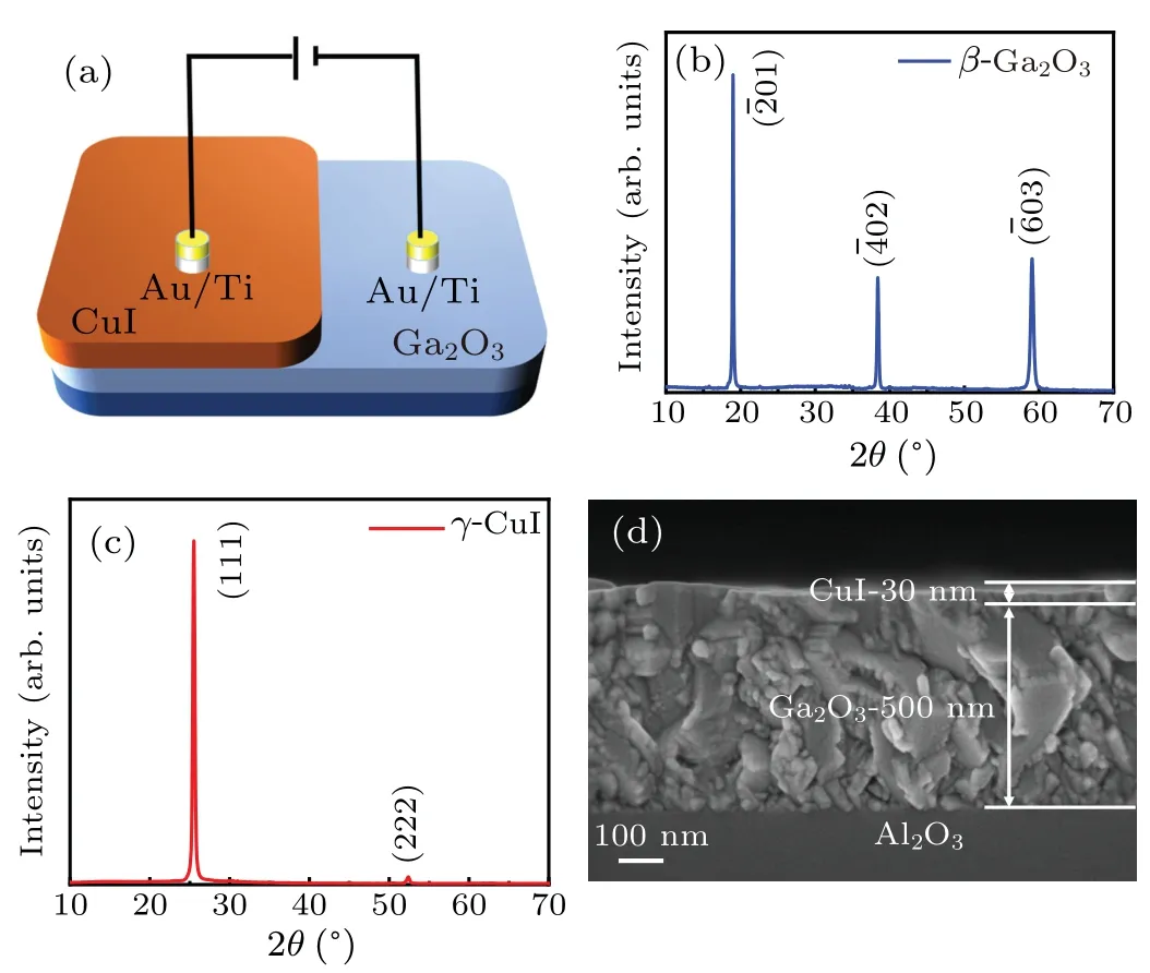
Fig.1.Device morphology characterization (a) The three-dimensional schematic diagram of device structure, (b) the XRD pattern of β-Ga2O3,(c)the XRD pattern of γ-CuI,and(d)the cross-sectional SEM image of the heterojunction structure device.
To investigate the optoelectrical characteristics of the device, 4200 digital sourcemeter instrument was employed.In order to verify the effect of junction effect on device performances, two single-layer thin film metal–semiconductor–metal (MSM) devices were fabricated and their performance were tested.The current–voltage (I–V) characteristics of β-Ga2O3and γ-CuI MSM devices are shown in Figs.2(a) and 2(b), respectively.TheI–Vcurves of the two MSM devices in the dark and under UV light illuminations are almost linear,suggesting both decent Ohmic contacts.γ-CuI MSM device has a large dark current(up to 4.0µA at 5 V),and the current becomes larger(up to 25.0µA at 5 V)when 254-nm UV light is turned on.While,in comparison,the β-Ga2O3MSM device has a small dark current (only 0.27 pA at 5 V), and the current becomes larger(86.3 nA at 5 V)under 254-nm UV light illumination.According to the electrical results by measurements in Figs.2(a)and 2(b),we could obtain the conductivities of 0.173 µS·cm−1(254-nm UV light), 1.24×10⁻⁷µS·cm−1(dark) for Ga2O3, and 51.3 µS·cm−1(254-nm UV light),8.7µS·cm−1(dark)for CuI,respectively.Therefore,the conductivity of CuI thin film is higher than Ga2O3, apparently.Ga2O3is a typical n-type transparent semiconducting oxide,and its conductivity is relatively low in the dark.However,due to the high absorption of light at 254-nm wavelength, photogenerated carriers are generated,and the conductivity is significantly improved after illumination.For the CuI film, a good Ohmic contact is achieved and it also has absorbance at 254-nm wavelength light (far weaker than Ga2O3), so it has high conductivity under light/dark conditions.
Figure 2(c) shows theI–Vcharacteristic curve of γ-CuI/β-Ga2O3heterojunction device.The dark current of the device fluctuates in a low range(0.1 pA–2.0 pA),and the device exhibits obvious rectification effect and photovoltaic effects under the irradiation of UV light with the illumination intensity of 500µW·cm−2.When the biasing voltage is −5 V,the dark current of the device is as low as 0.47 pA, the photocurrent is −50.93 nA, and the PDCR reaches as high as 1.08×10⁵.The asymmetrical photo responses at either positive or negative biases voltage show that the heterojunction structure has rectification effect.It can be seen from theI–Vcurve that the open circuit voltage (VOC) of the device is about 0.69 V, and it still responds to the UV light irradiation of 254 nm at zero bias(the photocurrent of −2.69 nA),owing to the achievement of photovoltaic effect in the Ga2O3/CuI heterojunction.
When the p–n junction is illuminated, the absorption of photons by the device will generate photo-generated carriers,and the intrinsic carriers will diffuse to the vicinity of the junction, drift under the action of the internal electric field, and complete the electron–hole pair separation,thus form a potential difference near the p–n junction boundary and generating photocurrent.In addition,the photo-generated carriers obtain greater energy under the acceleration of the electric field in the junction region and further collide to produce more carriers,thus generating the gain of the photocurrent.Therefore,the device has the potential to be a self-powered photodetector.

Fig.2.The I–V characteristics of (a) Au/Ti/γ-CuI/Ti/Au MSM device, (b) Au/Ti/β-Ga2O3/Ti/Au heterojunction device, and (c) Au/Ti/β-Ga2O3/γ-CuI/Ti/Au heterojunction device in the dark and under light illumination with an intensity of 500 µW·cm−2. The insets in panels (a) and (b) show the corresponding structure diagrams of each MSM device. The inset in panel(c)shows the dark current of less than 1 pA.
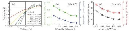
Fig.3.(a)The I–V response curves of γ-CuI/β-Ga2O3 heterojunction devices under different illumination intensities. Panels(b)and(c)are the curves of the responsiveness and specific detection rate of the device with different illumination power densities under the biasing voltages of 0 V and 5 V,respectively.
TheI–Vcharacteristics of γ-CuI/β-Ga2O3heterojunction device was further explored,and theI–Vresponses of the device under different illumination intensities were measured,as shown in Fig.3(a).Figures 3(b) and 3(c) show the changes of responsivity and specific detection rate of the device with different illumination power densities.It can be seen from the image that the photo response of the device changes regularly with the change of illumination power density.These curves show that the device can operate stably under different light intensities,and the photo response of different light intensities has a certain degree of differentiation.
TheI–tresponse of the device under different conditions is investigated.Figures 4(a) and 4(b) show theI–tresponse curves of 254 nm, under 500-µW·cm−2light, different bias voltages and 254 nm, 0-V bias voltage, different light intensities, respectively.As can be seen from Fig.4(a), under a certain illumination power density,the photocurrent increases regularly with the increase of bias voltage.In this figure, under 500-µW·cm−2illumination, in the range of 0 V–5 V, the photocurrent increases by about 10 nA for every 1-V increase of voltage.In addition,the device also shows a fast and stable response speed.This kind of good photoelectric characteristic is beneficial to improve the performance of photoelectric detector.Figure 4(b) shows a test of the device’s self-supply performance.In the absence of applied bias voltage, the device still exhibits a good optical response to 254-nm light,and the nanoscale photocurrent is competent to realize the function of photodetector in the case of self-powered.
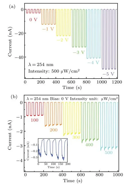
Fig.4.The I–t response curves of (a) to the 254-nm UV light with an intensity of 500µW·cm−2 under different bias voltages and(b)to the 254-nm UV light with different intensities under a bias voltage of 0 V.The inset of (b) shows the I–t response curve of a heterojunction device with a light intensity of 1µW·cm−2 at a 5-V biasing voltage.
TheI–tresponse of the device under small light intensity is also studied.Figure 4(b)shows theI–tresponse of the device at a light power density of 1 µW·cm−2.It can be seen from this figure that the device still generates a clear and observableI–tresponse to 254-nm light (the photocurrent is in the order of 0.1 nA) even under the low light intensity, indicating that the device has the potential to realize UV detection under the low light intensity.

Fig.5.Panels (a) and (b) respectively show the transient response and fitting results of the heterojunction device under the bias voltage of 3 V and the light power density of 500µW·cm−2 at 254-nm and 365-nm ultraviolet light.The data points are the transient response of the heterojunction device,and the lines are the fitting results.
The transient response of γ-CuI/β-Ga2O3heterojunction devices was investigated.Figures 5(a)and 5(b)shows the transient response and fitting results of the device under UV light at 254 nm and 365 nm respectively.The process of current rise and decay of the device is fitted, and the second-order exponential equation used to fit theI–tcurve:

whereI0is the steady-state photocurrent,AandBare constants,Tis time, and τ is the relaxation time constant.The rise time(τr)and decay time(τd)of the ultraviolet response of different bands are fitted under the same bias voltage of 3 V.At 254-nm light,the rise time(τr)and decay time(τd)are 0.762 s and 1.741 s, respectively.At 365 nm, the rise time (τr) and decay time(τd)are 10.709 s and 7.241 s,respectively.This indicates that the device has a faster response at 254 nm than at 365 nm.By the irradiation of 254-nm light, photo-generated carriers mainly come from valence–conduction band transition.However, by the irradiation of 365-nm light, the generation of photo-excited carriers are only from the defect–conduction band transition.During the photo-excited process,valence–conduction band transition is the main way.So, theIphotounder 254-nm light illuminations is much larger than that of 365-nm UV light.Meanwhile, some of the photo-excited carriers may well be captured by the trapping states in film.For the decaying process, the recombination of the carriers determines the decay time, and the fast decay speed is fact owing to the less trapping and the trapping states would be released and recombined.[28,29]What is worthy to be noted is that the irradiated source is a monochromatic lamp which could emit 254-nm UV light.When performing theI–tmeasurements, the UV lamp may illuminate the whole surface of the heterojunction photodetector.The light intensity could be changed by tunning the distance between the device and the lamp, where the intensity can be read through a display instrument.The optical switching behavior is owing to the reaction between the 254-nm and 365-nm UV light and the semiconductors in this heterojunction,[30]the incident photons excite the photo-generated electron–hole pairs for achieving the time-dependent optical switching phenomenon,as the UV lamp was turned on and turned off.
The spectral response range of γ-CuI/β-Ga2O3heterojunction device was measured, as shown in Figs.7(a) and 7(b).The spectral responsiveness with the cutoff wavelength of 410 nm proves that it has a certain broadband UV sensing capability.The UVC/UVA inhibition ratio(R225/R400)of the device is 5.58×10², which shows a certain spectral selectivity.In the spectrum,RandDhave obvious attenuation at 255-nm and 410-nm light,which is consistent with the absorption cutoff wavelengths of Ga2O3and CuI.Ga2O3response positively to UVC light, but less response to UVA light; while CuI showed stronger carrier productivity under UVC light.Therefore, β-Ga2O3/CuI heterojunction has a high photo response in the UVC region and a low photo response in the UVA region[24]at 0 V and 5 V,as displayed in Fig.6.
In order to confirm the role played by γ-CuI/β-Ga2O3heterojunction structure, the intrinsic physical mechanism of device operation was explained by the diagram of carrier transport mechanism and heterojunction band, as shown in Fig.7.It can be seen from the band diagram that there is a certain difference betweenEF(N)andEF(P)when n-type and p-type semiconductors exist alone.When n-type and p-type semiconductors are in close contact,electrons will flow from the high Fermi level to the low Fermi level, and the holes will flow in the opposite direction.At the same time, an internal electric field is generated.The direction of the internal electric field is from n region to p-region.Under the action of the internal electric field,EF(N)will move down together with the whole band in the n-region,andEF(P)will move up together with the whole band in the p-region,until the Fermi levelEFis leveled toEF(N)=EF(P),and the flow of charge carriers stops.At this time, the conduction band and valence band of the junction region bend accordingly,forming a potential barrier.

Fig.6.Spectral response curves of heterojunction devices at 5-V bias voltage(blue dot line)and 0-V bias voltage(red dot line).

Fig.7.The band diagrams of γ-CuI/β-Ga2O3 heterojunction under 254-nm ultraviolet light(a)and(b).
It is reported that when the band gap of Ga2O3is 4.86 eV,the valence band (VB) value is 7.95 eV and the conduction band(CB)value is 3.09 eV.When the band gap value of CuI is 2.98 eV,the valence band(VB)value is 2.22 eV and the conduction band(CB)value is 5.20 eV.The band structure of the heterojunction can form a typical type-II heterojunction.The diffusion and movement of the intrinsic charges cause band bending, creating a depletion layer at the interface.Since the photon energy is larger than the band gap value(hc/λ >Eg),when the heterojunction is irradiated by ultraviolet light of λ < 255 nm, the ground state electrons in VB in CuI and Ga2O3can be excited by absorbed photons and further transition into CB.Meanwhile, the photogenerated electron–hole pair in the depletion layer is separated by the built-in electric field near the heterojunction interface.The electrons are transferred from CB of CuI to CB of Ga2O3,and the holes are transferred from VB of Ga2O3to VB of CuI.
However, it should be pointed out that the optical response performance of the device is different in the UVA region and the UVC region.The device has a high responsivity in the UVC region (λ <255 nm), but the responsivity is slightly reduced at 255 nm< λ < 10 nm.This is because the energy ofhc/λ is low, the VB ground state electrons of Ga2O3cannot be excited,and the concentration of photogenerated carrier is less than that in the UVA region,as a result of the slightly worse performance.
4.Conclusions
In summary, we successfully prepared β-Ga2O3thin films on Al2O3substrate by MOCVD method, and then prepared γ-CuI/β-Ga2O3heterojunction by spin coating CuI thin films on Al2O3substrate.When the bias voltage is −5 V,the dark current and photocurrent of the detector are 0.47 pA and −50.93 nA,and the ratio of light-to-dark current reaches 1.08×10⁵.At 254 nm, the rise time (τr) and decay time (τd)are 0.762 s and 1.741 s,respectively,indicating a fast response speed.TheI–ttest shows that the device has good stability and response speed under different illumination power densities and bias voltages.In addition, thanks to the heterojunction structure and internal photoelectric effect,the device can work under unbiased voltage,and has the potential to become a self-powered photodetector.In conclusion,this β-Ga2O3/γ-CuI heterojunction wide ultraviolet photoelectric detector has a broad application prospect in the field of multispectral applications and self-powered energy-saving devices due to its excellent performance.
Acknowledgement
Project supported by the National Natural Science Foundation of China(Grunt No.61774019).
猜你喜欢
杂志排行
Chinese Physics B的其它文章
- High-sensitive terahertz detection by parametric up-conversion using nanosecond pulsed laser
- High efficiency,small size,and large bandwidth vertical interlayer waveguide coupler
- High-fidelity resonant tunneling passage in three-waveguide system
- An analytical model for cross-Kerr nonlinearity in a four-level N-type atomic system with Doppler broadening
- Determine the physical mechanism and source region of beat wave modulation by changing the frequency of high-frequency waves
- Estimation of co-channel interference between cities caused by ducting and turbulence