Light Enhanced Absorption of Graphene Based on Parity-time Symmetry Structure
2022-01-23YILingjunLIChanghong
YI Ling-jun, LI Chang-hong
(College of Electronic Information, Qingdao University, Qingdao 266071, China)
Abstract: To enhance the absorption of graphene for optical waves in near-infrared communication wavelengths, a graphene-based absorber based on a periodic parity-time(PT) symmetry structure was proposed, which consists of the top graphene layer and the underlying periodic PT-symmetry unit. The absorption properties of graphene in the wavelength range of 1 450-1 650 nm are systematically studied by the transfer matrix method(TMM). The results show that by optimizing the graphene composite PT-symmetry micronano structure parameters, a 35-fold absorptance enhancement was achieved for the normal incidence near-infrared light in the studied wavelength range as compared to the free-standing graphene absorption. Meanwhile, for the oblique incidence near-infrared light with angle ranging from 0° to 30°, the average absorptance of the TE and TM polarization light is also enhanced by 19.7 and 54 folds, respectively. The structure has high-intensity absorption characteristics for the near-infrared light, which can be widely used in the design of devices such as absorbers, photodetectors and infrared optical sensors.
Key words: parity-time symmetry; graphene; near-infrared; transfer matrix method
1 Introduction
Optical absorber has been extensively used in photoelectric conversion system, photoelectric detection, military stealth and other fields. Therefore, improving the absorptance of the absorber for a specific band of light wave has always been the focus of scholars[1-5]. Graphene, as one of the most promising two-dimensional nanomaterials, exhibits excellent electrical and optical properties, and consequence, graphene-based absorber has been attracting increasing interest, especially in the development of efficient absorbers based on graphene and other one-dimensional photonic crystals (1D-PC)[6-10]. For instance, Gaoetal. proposed a visible full-band optical wave absorber using graphene and 1D-PC composite structure, and a full-band absorptance of the visible optical band can reach 0.88[11]. Zhuetal. also designed a composite structure composed of the heterogeneous structure of the graphene and photonic crystal(PC),by adjusting the external magnetic field and Fermi energy, each absorption band can have an absorption of more than 99%, and under certain conditions, a near-perfect 100% absorption can be achieved[12]. Wuetal. propose a 1D graphene-based multilayer structure which composed of traditional dielectric material and graphene, the absorptance of the structure can be maintained higher than 80%[13]. For designing graphene-based optical devices with excellent integrated properties, such as optoelectronic detector and optical communication device, the absorptance of graphene needs to be further enhanced.
When the conventional PC structure is used to improve the graphene absorptance, the structure has no gain effect on absorbed light waves. Even if the structure achieves perfect absorption of the light wave in the research wavelength, it still affects the practical use of the structure for the weak light wave signal. While for the PC structure satisfying the parity-time(PT) symmetry conditions[14], the unique optical transmission and reflection phenomena will be generate[15-17], and therefore the PT-symmetry PC structure could be also an excellent option to be used to heighten the absorption of graphene compared with the conventional PC structure.
Therefore, in the current paper, inspired by the fantastic optical transmission characteristic of the PT- symmetry structure, a novel graphene-based PC structure was developed based on the well-established theory of PT-symmetry. By utilizing the transfer matrix method(TMM), we have theoretically studied the effect of rear PT-symmetry structure on the absorption properties of top graphene layer. The efficient graphene absorption was obtained by fine PT-symmetry microcavity design and detailed parameter analysis and optimization. Compared the conventional PC structure, the proposed structure not only has high absorption properties, but also has attractive advantages such as simple structure and small mode volume, which provides a reference for the design and preparation of graphene-based optical devices.
2 Model and Theoretical Calculation
The overall structure were designed as shown schematically in Fig.1, each dielectric layer can be simply represented as G(AB)Nin Fig.1(a) or as G(AB)Nin Fig.1(b). Thereinto,Nrepresents the unit cell number of the rear PT-symmetry structure, G deputies graphene layer, which was placed to the foreword-side of the PT-symmetry photonic crystal. For the underlying structure, the gain-loss layers were formed by doping quantum dots in the substrate dielectric silica, denoted by A and B, respectively. The refractive index of A or B layer can be described as[18]:
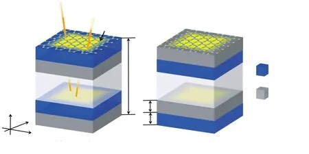
Fig.1 (a)Schematic diagram of the 1D PT-symmetry PC structure G(AB)N. (b)Schematic diagram of the 1D PT-symmetry PC structure G(BA)N.
nA=nSiO2+nii,
(1)
nB=nSiO2-nii,
(2)
wherenAis the refractive index of the loss layer,nBis the refractive index of the gain layer.nSiO2andniare the real and the imaginary component of the refractive index respectively. The imaginary componentnicharacterizes the relationship between the system gain, the concentration of doping quantum dots and the distribution excited state quantum dots. When the underlying structure satisfies the PT-symmetry condition, the absolute value of the imaginary componentniof layer A is tantamount to layer B.nSiO2denotes the dielectric constant of the basal silica, which can be described by the Sellmeier dispersion relation as a simple approximation[19]:
(3)
whereλis the wavelength,Ciis the oscillator strength constant, the values ofC1,C2,C3are 0.7, 0.41, 0.9, respectively;λiis the characteristic oscillator wavelength, the values ofλ1,λ2,λ3are 68, 116, 9 896 nm, respectively.
For the graphene layer on the top, the optical properties are closely related to its complex surface conductivityσG. Its effective dielectric constant can be expressed as[2]:
(4)
whereε0is the vacuum dielectric constant;dG=0.34 nm is the thickness of monolayer graphene;ωis the angular frequency of incidence light;σGis the surface conductivity of graphene, under random-phase approximation, which can be expressed as:
σG=σin+σout,
(5)
thereinto:
(6)
(7)
where ћ=h/2π is the reduced Planck constant;eis electron charge;kBis Boltzmann constant;T=300 K is the Kelvin temperature;μis the chemical potential, which determined by the electron concentration and can be controlled by the gate voltageV[20];τ=0.5×10⁻¹⁴s denotes the relaxation time of graphene layer.
The transmission matrix method(TMM) is used to study the absorption characteristics of the structure in this paper. Based on the system of Maxwell equations, the relationship between adjacent space fields can be calculated by the TMM, the transmission matrix of theith monolayer can be defined by the following matrix[21]:
(8)

(9)
(10)
(11)
then, the transmissionTtotal=|ttotal|2and reflectionRtotal=|rtotal|2can be obtained, respectively.
The absorption of graphene layer can be described by the following two processes.Firstly, when incidence light transfers into the underlying PT-symmetry photonic crystal structure through the graphene layer,the initial absorption of incidence light is caused by graphene. And secondly, the Bragg reflection of incidence light is produced by the bottom layer PT-symmetry photonic crystal structure, when the reflected light passes through the graphene layer, ignoring other scattering losses in this scenario, the absorption of graphene can be derived by Poynting vector expression[6]:
(12)
whererPTandtPTrepresent the reflection coefficients and transmission coefficients of the underlying PT-symmetry structure, respectively.
3 Numerical Results and Discussion
We focus on the incidence light absorption properties of graphene for important infrared communication wavelength, and choseλ0=1 550 nm as the center wavelength in this paper. Meanwhile, to make the rear structure meet the PT-symmetry condition, the refractive index of AB layer meets the conjugate symmetry condition, the optical thickness of AB layer should be equal, from which we determined the optical thickness of the AB layer asdA=dB=nSiO2/4n0. We first take the imaginary componentni=0.15 andN=5 for the underlying PT-symmetry PC, the chemical potentialμ=0.38 eV, thicknessdG=0.34 nm for the monolayer graphene. Other structure parameters are given in part 2.
In order to research the effect of structure type on graphene absorption and the absorption properties of PT-symmetry structure without graphene layer. In Fig.2(a), we plot the graphene absorption spectra of different structures and the absorption spectra of PT-symmetry structure (BA)Nand (AB)Nwithout graphene layer. From Fig.2(a), we observe that there is an obvious absorption peak, with a FWHW of nearly 200 nm (from 1 450 nm to 1 650 nm), which is centered at the wavelength 1 550 nm, the difference is that the absorption of the structure G(BA)Nis significantly greater than that of the structure G(AB)N. Meanwhile, for the PT-symmetry structure (BA)Nand (AB)N, The structure exhibits negative absorption due to the gain effect on the incidence light, and thus enhancing the absorptance of the graphene layer. Next, we calculate the average absorptance of graphene in the wavelength range of 1 450-1 650 nm for different period numberN. Results presented in Fig.2(b) show that for the selected wavelength range, the graphene absorptance of structure G(BA)Nis greater than that of structure G(AB)Nat different periodN, and the average absorptance is the largest whenN=6.
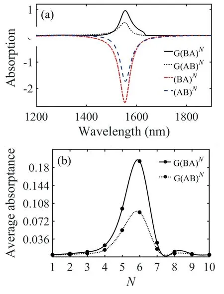
Fig.2 (a)The absorption spectra of graphene and PT-symmetry units under different structures. (b)The average absorptance of graphene as a function of the period number N for different structures.
For better illustrating the difference in the average absorptance of graphene layers in the two structures for the same period, we plot the transmission and reflection spectra of structure G(AB)Nand structure G(BA)Nwhen the periodN=6, respectively, and the results are shown in Fig.3(a) and Fig.3(b). As can be seen from Fig.3, the transmission at differents wavelengths is almost identical for both kinds of the structures, but the reflection exhibits some numerical difference. In the wavelength range of 1 450-1 650 nm, the average reflection of structure G(BA)Nis significantly larger than the structure G(AB)N. The reason for this difference can be explained by the group velocity of light waves in different media. First of all, when the group velocity of light in the gain medium is lower than the lossy medium, there will be a longer action time between light wave and the gain medium, then external pump energy will be more converted into the electromagnetic energy of incidence light, thus producing the phenomenon of increased reflection[22]. The gain and loss of the light wave in the two structures are unbalanced, and consequencely, the reflection amplification occurs in some wavelength range.
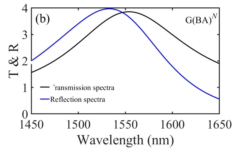
Fig.3 (a)The transmission and reflection as a function of the light wavelength for the structure G(AB)N. (b)The transmission and reflection as a function of the light wavelength for the structure G(BA)N.
At the same time, the group velocity of the gain medium in structure G(BA)Nis smaller than that in structure G(AB)N, so the reflectivity of structure G(BA)Nis larger.
We can know from Eq.(12) that the reflection of the underlying structure is the key factor affecting graphene absorptance. When the structure reflection is enhanced, it will cause further enhancement of the absorptance of graphene to the incidence light. the absorptance of graphene is more efficient in structural G(BA)Ncompared to structural G(AB)N. Therefore, the structure G(BA)NandN=6 is selected for the following studies.
Fig.4(a) depicts the eigen-spectra of the structure G(BA)Nwith the change of the imaginary componentni. We can observe from Fig.4(a) that asniincreased, the imaginary component of the transfer matrix eigenvalues fluctuate between -1 and 1, and tend to zero whenniis greater than 1.04, which indicates that the imaginary component of the transfer matrix eigenvalues ceases to be imaginary whenniis greater than 1.04. For our optimized system parameters,ni=1.04 is the PT-threshold of the structure G(BA)N. For the values ofnigreater than the PT-threshold, the structure will no longer have an amplification effect on the incident light[23]. Therefore,it is meaningful to consider only the structure eigenvalues less than thenivalue corresponding to the PT-threshold value.
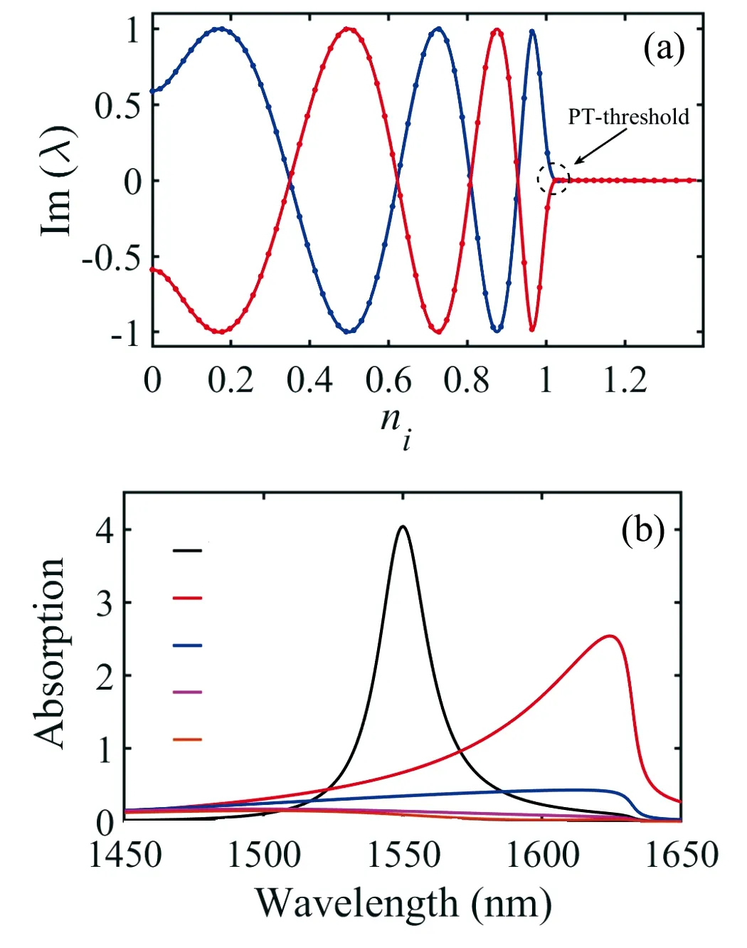
Fig.4 (a)Eigen-spectra of the transfer matrix for the structure G(BA)N. (b)The absorption spectra of graphene under different imaginary components of the refractive index.
The matrix eigenvalue of the imaginary part partly reflects the level of action of the structure on the incidence light waves, at some specific matrix eigenvalues, the structure will produce exotic optical phenomena[23], which will enhance the graphene absorptance of the light wave. In Fig.4(b), we plot the absorption spectrum of the graphene at these discretenivalues when the matrix is near ±1, it can be seen that for the structure G(BA)N, the absorption of graphene shows great distinctions as we change the imaginary componentni. For clearly illustrating the effect ofnion graphene absorptance, Tab.1 lists the matrix eigenvalue corresponding to different discrete pointsniand the average absorptanceAin the wavelength range from 1 450 nm to 1 650 nm.
Tab.1 Matrix eigenvalue and average absroption of the structure G(BA)N under different ni
As can be seen from Tab.1, for eigenvalues where the imaginary part tends to -1 or 1, only when the real part tends to 0 (ni=0.20), the average absorptance of graphene to light waves in the wavelength range from 1 450 nm to 1 650 nm reaches the maximum. Therefore, we can determine the imaginary componentniof AB layer in the PT-symmetry structure based on the matrix eigenvalue, thereby enhancing the absorptance of graphene.
The wavelength value corresponding to the right edge of the absorption band is related to the chemical potential of graphene[13], so changing the chemical potential of graphene will affect the graphene absorptance. As can be seen from Fig.3, the enhancement effect of the proposed structure on graphene absorption is more obvious in the wavelength range of 1 450-1 650 nm. In order to study the influence of the chemical potential on graphene absorptance in the wavelength range, we determine the chemical potential from 0.38 eV to 0.42 eV according to the change rule of the graphene absorption band in literature[13]. In Fig.5(a) and (b), we plot the absorption spectrum of the structure G(BA)Nand the single layer grapheneversuswavelength at different chemical potentialμ=0.38, 0.39, 0.40, 0.41, 0.42 eV, respectively. By comparing Fig.5(a) and (b), it can be seen that for the proposed structure G(BA)N, the graphene absorptance is greatly enhanced under the same chemical potential. Meanwhile, it can also be seen that the right absorption band edge has obvious red shift and the absorption band broadens withμdecreasing.
Tunability of the graphene absorption by the chemical potential could be explicatedviathe dependence of the graphene refractive index on its chemical potential. Taking Eqs.(4)-(7) into account, it is obvious that the absolute value of theεGincreases when we increase the chemical potential, which in turn makes an increase in the total refractive index of the graphene layer. For confirming the phenomenon that the edge of absorption band red shift with the increase of chemical potentialμmore intuitively, the variation curves of the real and imaginary parts of the graphene dielectric constant are given in Fig.5(c) and Fig.5(d), which are plotted with the chemical potential changes from 0.38 to 0.42 eV, respectively. It can be seen from Fig.5(c) and (d) that for different chemical potentials, the spike in the real part of the graphene dielectric constant(realεG) corresponds to the sudden fall of the imaginary part(imaginaryεG), furthermore, as the chemical potential decreases, the feature of the real and imaginary parts of the graphene permittivity have a celerity red shift in the investigated wavelength range from 1 450 nm to 1 650 nm, which is the dominating reason for the edge of absorption band red shift with the increase of chemical potentialμ.
Therefore, combining the change curves of the real and imaginary parts of the graphene refractive index in Fig.5(c) and (d), we can conclude that, to allow the structure to obtain a better absorption effect, the chemical potential value should be taken within the range of less than 0.38 eV. Without loss of generality, we choose the chemical potentialμ=0.38 eV for the following calculation.
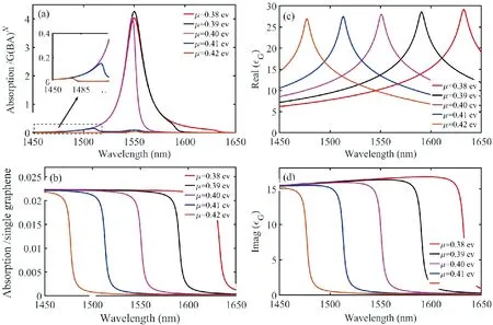
Fig.5 (a)The absorption spectra of single-layer graphene with different chemical potential μ. (b)The absorption of single-layer graphene with different chemical potential μ. Real parts(c) and Imag parts(d) of the complex permittivity of graphene for different chemical potential μ.
The dielectric constant of graphene is not only related to the chemical potential, but also to the external temperature. We further calculated the absorptance of graphene at different temperatures, the results shown that as the temperature changes from 250 ℃to 400 ℃, the average absorptance of graphene from 1 450 nm to 1 650 nm is close to 0.812, the change of external temperature has little effect on the absorption of graphene. Therefore, the working environment of the proposed structure is not strictly limited by temperature.
In the following section,we investigate the influence of incident angle of light wave on the absorption properties of graphene in TE and TM modes(see Fig.6). The graphene absorber designed in this paper has a PT-symmetry periodic structure, therefore, when the incidence light transfers into vertically(θ=0°), the absorber has a very high polarization insensitivity, the average absorptance obtained by incidence light with TE polarization wave and incidence light with TM polarization wave are almost identical, which can reach 0.812(35 folds than free-standing graphene). When the incidence angleθof incidence light changes, the absorption of TE polarization wave and TM polarization wave by the absorber should be discussed respectively.
Fig.6(a) plotted the absorption of TE polarization wave as a function of wavelength at different incidence angles from 0° to 30°. It can be seen that with the increase of incidence angle, the absorption peak moves to the short-wave direction(from 1 550 nm to 1 460 nm), meanwhile the absorption peak decreases from 4.038 to 0.348, and the average absorptance of light wave(from 1 450 nm to 1 650 nm) decreases from 0.813 to 0.123. As shown in Fig.6(b), for the TM wave, the absorption peak also moves to the shortwave direction with the increase in the incidence angle, but the difference is that the absorption peak and the average absorptance increase first and then decrease with the increase of incidence angle, when the incidence angle is around 20°, the absorption peak and the average absorptance reach the maximum of 56.63 and 2.578, respectively. According to the analysis of the results, when the incidence angle changing from 0° to 30°, the average absorptance of the TE and TM polarization lights can be enhanced by 19.7 and 54 folds, respectively. Therefore, for TM polarization light, graphene has the highest average absorptance at wavelengths 1 450-1 650 nm, which indicates that the structure is most sensitive to TM polarization light, and it should be pointed out that the larger the average absorptance value is, the better the absorption performance of graphene-based device is.
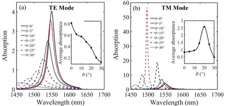
Fig.6 (a)The absorption of graphene in TE mode as a function of the light wavelength for different incidence angles. (b)The absorption of graphene in TM mode as a function of the light wavelength for different incidence angles.
Since the underlying structure satisfies the PT-symmetry conditions, the absorptance of the top graphene layer is greatly enhanced for the studied wavelength range. Therefore, compared with other similar structures, the structure G(BA)Nproposed in this paper has excellent absorotion performance. For the graphene absorber proposed by Liuetal., although the absorptance is also improved, the absorption bandwidth is very small[24], therefore, for graphene-based photodetectors, the detection of light waves in a larger bandwidth cannot be realized. Meanwhile, it is worth noting that this paper mainly investigates the enhancement effect of the structure on graphene absorptance in the near-infrared band from 1 450 nm to 1 650 nm, which is an important communication band at the center of 1 550 nm. Therefore, we optimized the parameter of the structure on the basis of the central wavelength of 1 550 nm so that the resonance coupling effect of the structure at the central wavelength is the strongest, so as to realize the enhancement of graphene absorptance. Therefore, enhanced absorption of graphene to light waves of other wavelengths can be realized by changing the location of the central wavelength and optimizing the structural parameters.
4 Conclusion
In conclusion, we studied the near-infrared optical absorption of graphene layer prepared on top of a 1D PT-symmetry PC theoretically. We found that the proposed absorber has excellent absorption in the 1 450-1 650 nm wavelength range, when the imaginary component of the refractive indexni=0.20, the period numberN=6, the graphene chemical potentialμ=0.38 eV, the average absorptance of graphene on the 1D PT-symmetry PC can be enhanced by about 35 folds under normal incidence light(for the TE and TM wave). The results also show that for the TE and TM polarization light with the incidence angle changing from 0° to 30°, the average absorptance can be enhanced by 19.7 and 54 folds, respectively. These characteristics indicate that our proposal has certain reference significance for the design of graphene-based photodetector, absorber as well as communication devices.
Response Letter is available for this paper at:http://cjl.lightpublishing.cn/thesisDetails#10.37188/CJL. 20210322.