Molecular beam epitaxy growth of monolayer hexagonal MnTe2 on Si(111)substrate∗
2021-12-22Lu卢帅Peng彭坤Wang王鹏栋Chen陈爱喜Ren任伟Fang方鑫伟Wu伍莹Li李治云Li李慧芳Cheng程飞宇Xiong熊康林Yang杨继勇Wang王俊忠Ding丁孙安Jiang蒋烨平Wang王利Li李青Li李坊森andChi迟力峰
S Lu(卢帅) K Peng(彭坤) P D Wang(王鹏栋) A X Chen(陈爱喜) W Ren(任伟)X W Fang(方鑫伟) Y Wu(伍莹) Z Y Li(李治云) H F Li(李慧芳) F Y Cheng(程飞宇)K L Xiong(熊康林) J Y Yang(杨继勇) J Z Wang(王俊忠) S A Ding(丁孙安) Y P Jiang(蒋烨平)L Wang(王利) Q Li(李青) F S Li(李坊森) and L F Chi(迟力峰)
1Institute of Functional Nano&Soft Materials(FUNSOM),Soochow University,Suzhou 215123,China
2Vacuum Interconnected Nanotech Workstation(Nano-X),Suzhou Institute of Nano-Tech and Nano-Bionics(SINANO),Chinese Academy of Sciences(CAS),Suzhou 215123,China
3Key Laboratory of Polar Materials and Devices(MOE),Department of Electronic,School of Physics and Electronic Science,East China Normal University,Shanghai 200241,China
4School of Physical Science and Technology,Southwest University,Chongqing 400715,China
5School of Nano-Tech and Nano-Bionics,University of Science and Technology of China,Hefei 230026,China
Keywords: molecular beam epitaxy,hexagonal MnTe2,band structure
1. Introduction
Two-dimensional(2D)materials have attracted extensive attention since the discovery of graphene.[1]When thinned to the monolayer limit, 2D materials will exhibit unique electronic and optical properties such as superconductivity[2–4]and charge density waves (CDW).[5–7]In particular, ferromagnetic and antiferromagnetic materials would be a significant addition to the family of 2D materials due to their potential application in the next-generation spintronic devices with stable storage, faster response, and low-power dissipation.[8]The recent experimental breakthrough was the observation of quantum anomalous Hall effect (QAHE) in intrinsic magnetic topological insulator MnBi2Te4,[9]in which the magnetism originates from the magnetic Mn–Te layers[10]with the high-ordered magnetism distribution in the crystal.[11]In the MnBi2Te4system, each Mn atom is bonded with six neighboring Te atoms,which form octahedral(1T)structure MnTe2.The monolayer MnTe2was predicted as a candidate for 2D ferromagnetic material.[12]To the best of our knowledge,no experimental investigation about the epitaxial growth of monolayer hexagonal MnTe2has been reported.
Manganese telluride (MnTe) has been demonstrated as a promising thermoelectric material.[13]NiAs-type MnTe(hexagonal MnTe, H-MnTe) bulk is a diluted magnetic material,exhibiting antiferromagnetic property with a N´eel temperature (TN) of 310 K.[14]And it is a p-type semiconductor with a small bandgap of 1.37–1.52 eV.[15]The lattice constant isa=b=4.158 ˚A,c=6.726 ˚A[16]and the magnetic order of H-MnTe has been determined to be in-plane ferromagnetic layers stacking antiferromagnetically along thecaxis.[17,18]Room temperature ferromagnetism was observed in thick MnTe film prepared by molecular beam epitaxy(MBE)technique.[19]There is no experimental report about the twodimensional limit of MnTe, where a Mn atom layer sandwiched between two Te layers. Recently, the DFT calculations suggest that when thinned the H-MnTe to the monolayer limit, MnTe2can stabilize as 1T-structure and is an intrinsic ferromagnetic metal.[12]There is a pyrite cubic structured three-dimensional MnTe2, which was reported to be a p-type semiconductor,[20]quite different from hexagonal MnTe, focusing on its potential thermoelectric applications.[21]Therefore, the experimental realization of the monolayer MnTe2is important and promising for 2D magnetism.
Here we report an epitaxial growth of high-quality hexagonal monolayer MnTe2on Si(111)-(7×7)substrate by means of MBE. The structure and component were characterized by combiningin-situscanning tunneling microscopy (STM),reflection high-energy electron diffraction (RHEED), lowenergy electron diffraction (LEED), angle-resolved photoemission spectroscopy(ARPES),and x-ray photoelectron spectroscopy (XPS). STM and RHEED measurements show an MnTe2monolayer with a lattice of∼4.1 ˚A and the height of∼5 ˚A on Si(111)substrates. A large bandgap of∼2.78 eV is observed with semiconducting properties in the MnTe2monolayer. Three hole-type bands with parabolic-type dispersion are observed by the ARPES measurements and the valenceband maximum (VBM) locates atΓpoint. Our work clearly shows the successful growth of a two-dimensional semiconducting MnTe2monolayer.
2. Experimental methods
Epitaxial growth of monolayer MnTe2on the Si(111)was carried out in a combined ultrahigh vacuum (UHV) system with a base pressure better than 3×10⁻¹⁰mbar. Prior to the film growth,the clean Si(111)-(7×7)substrates were obtained by multi-cycle flashing to∼1320 K.High purity Mn(99.98%)and Te (99.9999%) were co-evaporated from standard Knudsen cells(K-cell). The growth rate of the MnTe2film was estimated to be 0.05 ML/min,mainly determined by the flux of the Mn source. RHEED was used to monitor the crystallinity and surface morphology during the growth. The surface morphology and electronic structure were further characterized byin-situSTM at room temperature using a tungsten tip. The differential dI/dVspectra were acquired by standard lock-in techniques (f=973 Hz,T=300 K). All the STM images were treated by using the WSxM software.[22]
By transferring via the UHV tubes (base pressure better than 2×10⁻¹⁰mbar) in Nano-X, the band structure and surface component of the monolayer MnTe2can be measuredinsituby ARPES and XPS,respectively. Monochromatized He-Iαlight source (21.21 eV) was used in the ARPES measurement with a VG DA30L analyzer. The energy resolution and angular resolution were better than 30 meV and 0.1◦,respectively. XPS measurements were carried out by using a PHI 5000 Versaprobe II system equipped with a monochromatic AlKα(1486.6 eV)x-ray source. The core level and valance band structure spectra were calibrated against C–C 1s(binding energy is around 284.8 eV).
3. Results and discussion
Mn–Te compounds in bulk and thick films normally crystallize into NiAs-type MnTe with Mn:Te∼1 : 1. To stabilize monolayer MnTe2with Te termination, we introduced the molecular beam epitaxy method with the help of substrate and Te-rich atmosphere. Prior to the film growth, the Si(111)substrates were first degassed at 820 K for more than 10 h, followed by multi-cycle flashing at∼1320 K for 10 s each time. The sample temperature was monitored by an infrared pyrometer. After such procedure, atomically clean Si(111)-(7×7) surfaces can be obtained, confirmed by the sharp RHEED spots in Fig. 1(a). During the film growth,the Si(111) substrate was kept at 573 K. The flux ratio of Te/Mn was about 10:1. The RHEED pattern in Fig. 1(b)shows sharp streaky lines from a thin film and bright spots from the Si(111) substrate (aSi(111)∼3.85 ˚A), demonstrating epitaxial growth with an atomically flat surface. The lattice constant of the monolayer MnTe2can be estimated to be∼4.1 ˚A, just slightly smaller than the lattice constant of bulk H-MnTe (a=4.158 ˚A), quite different from the value obtained in DFT calculations.[12]The hexagonal LEED pattern in Fig.1(c)rules out the possibility of pyrite cubic structured MnTe2. No surface reconstruction was found. The fact of only one set of hexagonal LEED pattern indicates monolayer MnTe2with a single orientation, despite the high mismatch (∼8%) between the monolayer MnTe2and the substrate. Spots of the Si(111)substrate could not be observed after the surface was completely covered with monolayer MnTe2(see Fig.S1 in the supplementary material for details).
The STM image in Fig.1(d)shows the surface morphology of sub-monolayer MnTe2grown on Si(111). Similar to the monolayer WTe2[23]and WSe2,[24]distributed MnTe2islands were observed when the sub-monolayer was grown. All the islands exhibit the same height of∼500 pm, according to the line profile in Fig. 1(e). In the bulk of hexagonal MnTe, the thickness of the Mn–Te layer alongcdirection is∼1.68 ˚A.Given the height of the monolayer islands,the film could be Te–Mn–Te or Mn–Te–Mn–Te. To further confirm the structure and surface compounds,in-situXPS measurements were needed, as shown below. Figure 1(f) shows the typical dI/dVspectrum of the monolayer MnTe2. We can observe a big bandgap across the Fermi level. The VBM locates at−1.20 eV and the conduction-band minimum locates at 1.58 eV,indicating a bandgap size of∼2.78 eV.Such value is larger than the one in bulk H-MnTe(1.37 eV–1.52 eV).[15]But it is quite different from the predicted metallic property in DFT calculation.[12,32]Maybe it is due to the varied lattice constants. A small lattice constant of 3.8 ˚A was obtained in the DFT calculation.[12]
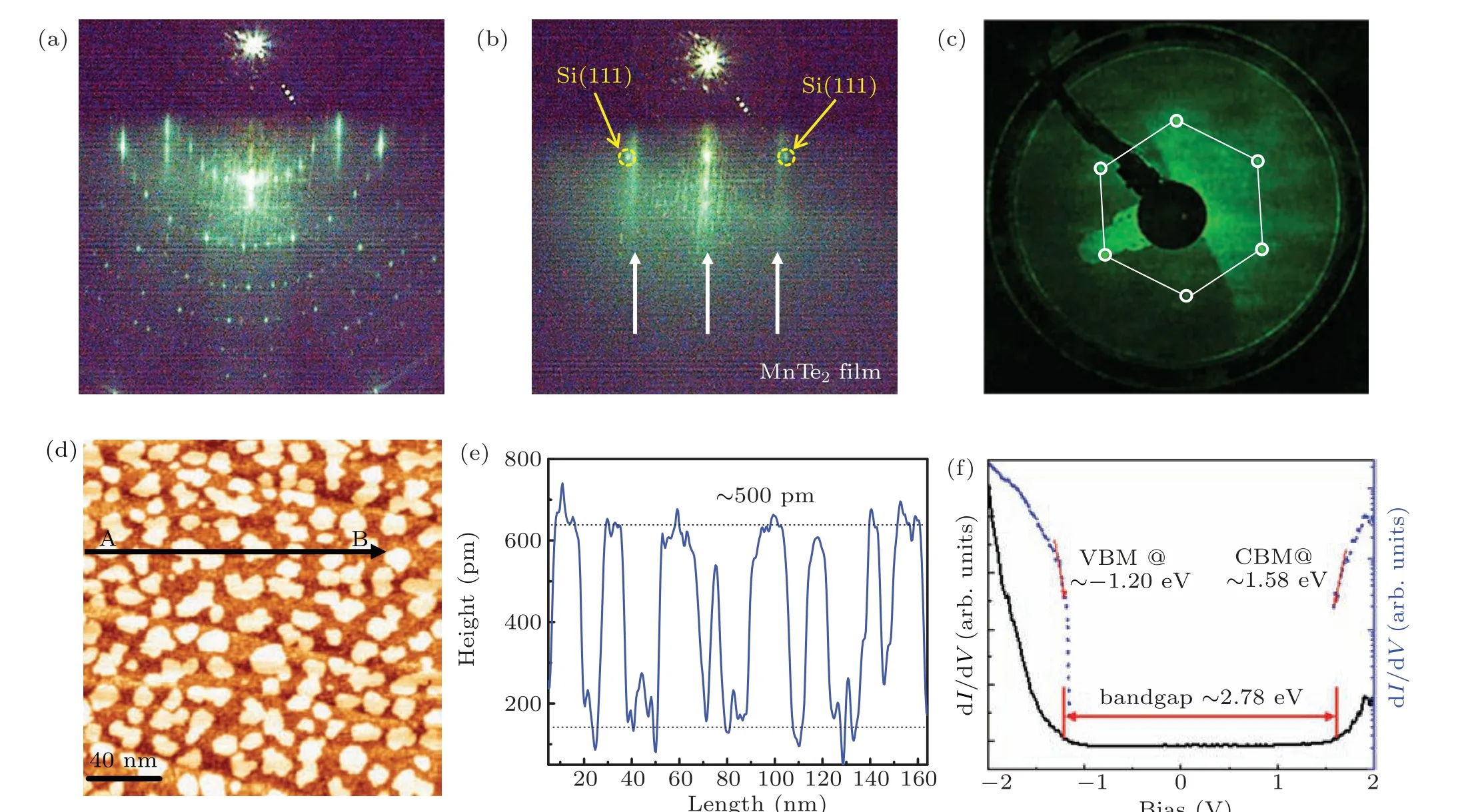
Fig.1. Growth of monolayer MnTe2 film on the Si(111)substrate. (a)RHEED pattern of the flashed Si(111)substrate,showing typical(7×7)reconstruction spots. (b)RHEED pattern of the sub-monolayer MnTe2. White lines mark the pattern of film, while the yellow dotted circles indicate the Si(111)substrate. (c)LEED pattern image of the monolayer MnTe2,clearly showing a hexagonal structure. (d)Large-scale STM image of 0.5 ML MnTe2, showing the surface morphology (200 nm×200 nm). Scanning condition: Vs =2.0 V, It =20 pA. (e) Line profile of the black arrow AB in panel (d), showing all the monolayer MnTe2 islands have with the same height of ∼500 pm. (f) Typical dI/dV spectrum on the monolayer MnTe2,showing the semiconducting gap size of ∼2.78 eV.Blue curve is the logarithmic plot.
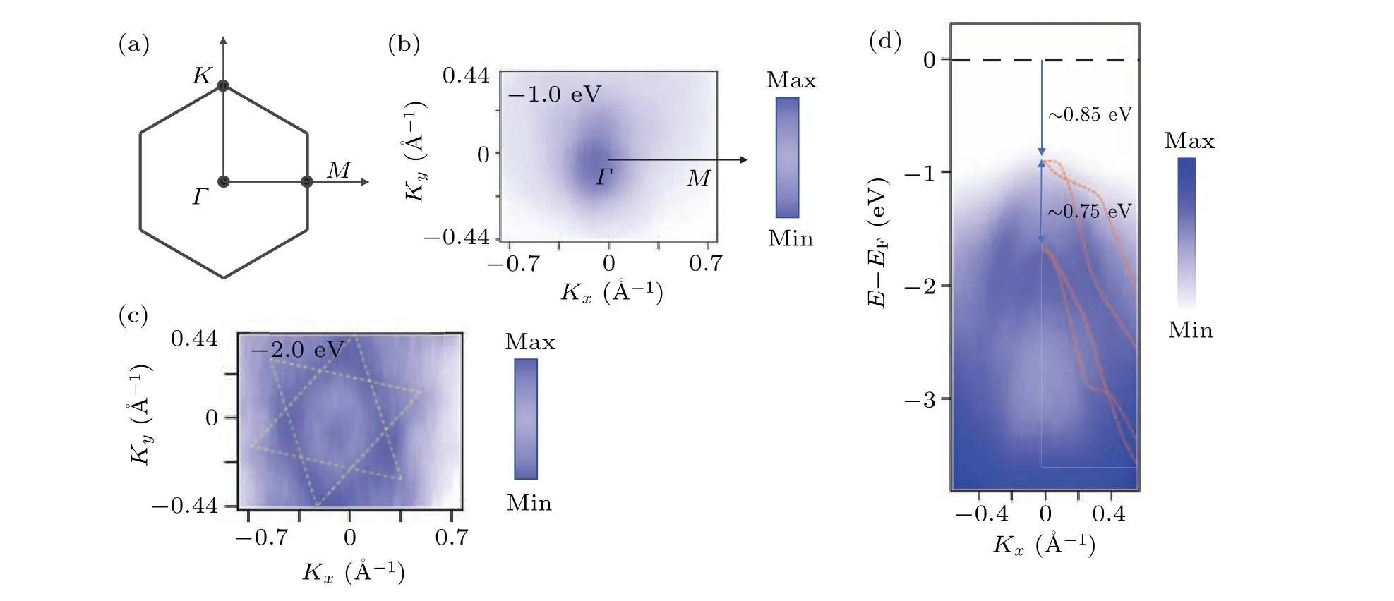
No oxidation signal from the monolayer MnTe2can be observed in the survey XPS spectrum(see Fig.S2 in the supplementary material)after the growth and transferring process.Figures 2(a)–2(c)show the XPS spectra of Mn 3s,Mn 2p,and Te 3d core-levels,respectively. In Fig.2(a),the Mn 3s spectra can be deconvoluted into two peaks due to the coupling of the nonionized 3s electron with 3d valence-band electrons in Mn,with the binding energies of 83.43 eV and 88.13 eV, respectively. The energy difference (∆E3s) is∼4.7 eV, indicating that the valence state of Mn is mainly +4 in the monolayer film.[25]Due to the complexity of Mn 2p spectrum with the splitting of 11.5 eV,we have performed a detailed deconvolution analysis in Fig.2(b). Peak 1 of 640.6 eV corresponds to the low charge state of Mnq+(0 According to the peak and the relative sensitivity factor,we can calculate the chemical composition, the atom ratio of([Mn]:[Te])∼1:2.6. Judging from the valence state of +4 and atom ratio of 1:2.6,we can conclude that the grown monolayer is MnTe2,as shown in Fig.2(f).The larger Te ratio in the samples should be ascribed to the Te passivation layer between MnTe2and Si(111) substrate, which offers an atomically flat template for the film growth by saturating the dangling bonds on the Si(111) substrate.[29]The Te passivation layer may be helpful for the growth of monolayer MnTe2with a large mismatch to Si(111)substrate. Such a Te-rich-atmosphere growth method has been widely used in the growth of Bi2Te3film on Si(111) substrate.[30]Figure S2(b) shows the cut-off edge of UPS spectra with the sample biased to−5 V. The work function (∼4.76 eV) of monolayer MnTe2can be calculated by using the formulaφ=hν −SECO−5, in which the secondary electron cut-off (SECO) is obtained from a linear extrapolation, as shown in the inset of Fig. 2(d). The valence band maximum of∼1.32 eV can also be extracted in Fig.2(e)by linear extrapolation,which agrees well with our STS measurement in Fig. 1(f). Figure S2(c) gives the band structure of monolayer MnTe, extracted from XPS and STS measurements. Thus, we can draw the constructed band diagram of the monolayer MnTe2on Si(111). Figure 2(f) shows the top and side views of the monolayer 1T-MnTe2respectively. The octahedral 1T structure is consistent with the previous DFT calculation results.[12] Fig.2. XPS measurements of the monolayer MnTe2 on Si(111). (a)–(c)The core-level spectra of Mn 3s,Mn 2p,and Te 3d. The spaced double peaks (∼4.7 eV) in Mn 3s suggest that the valence state of Mn is +4. The core-level spectrum of Mn 2p3/2 can be deconvoluted into four peaks. (d)UPS measurement of monolayer MnTe2,showing the work function of ∼4.76 eV.(e)Valence-band maximum of MnTe2 film. (f)Top and side view model of monolayer MnTe2. The blue and yellow balls represent Mn and Te atoms,respectively. Fig. 3. Electronic band structure of the monolayer 1T-MnTe2 on Si(111) substrate. (a) The Brillouin zone of monolayer MnTe2. (b) The momentum space mapping at the energy of −1.0 eV,near the VBM.(c)The momentum space mapping at the energy of −2.0 eV.(d)The band structure measured along Γ–M direction. To further explore the electronic structure of monolayer MnTe2/Si(111) heterostructures, we performed ARPES measurement at room temperature. To the best of our knowledge,ARPES observations on bulk or thin film MnTe materials have been rarely reported. Figure 3(a) shows the Brillouin zone of the hexagonal MnTe2monolayer. The momentum space mapping at−1.0 eV in Fig. 3(b) shows only hole pockets atΓpoint with VBM at∼−0.85 eV,consistent with the gaped structure obtained from the STS and XPS measurements. We notice that in bulk MnTe the VBM is also predicted atΓpoint theoretically.[31]The mapping at−2.0 eV in Fig. 3(c)shows a typical hexagonal structure with hole pockets. Figure 3(d)shows the band structure of monolayer MnTe2along theΓ–Mdirection. Three hole-type bands with parabolictype dispersion and“M”-shape dispersion at a deeper level are observed. Overall band shapes are similar to those of bulk MnTe[31]or 1T-MnTe2monolayer.[12,32]Here we find that the low two parabolic bands seem to overlap together. The energy difference between the upper parabolic bands and the lower ones is about 0.75 eV. The observed band structure is quite different from that of the Si(111)substrate,as shown in Fig. S3. Clean Si(111)-(7×7) substrate shows nearly linear dispersion along theΓ–Mdirection. The surface states of S1,S2, and S3 can be identified at 0.20 eV, 0.90 eV, and 1.8 eV below the Fermi level, respectively.[33]After the growth of monolayer MnTe2, no surface state and other band structures from Si(111) surface can be observed. According to previous DFT calculations,[12,32]monolayer MnTe2was predicted to be metallic. Our observations suggest monolayer hexagonal MnTe2exhibits semiconducting properties with considerable bandgap(∼2.78 eV)at room temperature, larger than that of bulk MnTe (1.37 eV–1.52 eV).[15]One possibility is the varied lattice constant. As predicted,[32]the lattice strain can open a bandgap in MnTe2monolayer. However, the predicted bandgap is much smaller than the one in our experiment,which deserves further detailed calculations. We would like to discuss more about the formation of hexagonal MnTe2monolayer. In previous MBE growth,thick MnTe film crystallized into NiAs-type phase on the Si(111)[19]and InP(111),[34]while the preparation of a monolayer thin film failed. As shown in Fig. S4, if further increasing the coverage, several islands with the height of∼330 pm were observed on the monolayer MnTe2,beside the second MnTe2layer with the height of∼670 pm. It demonstrates the competition between the formation of bulk MnTe and van der Waals layered MnTe2. The interaction with the substrate can stabilize the monolayer MnTe2. The successful grown monolayer MnTe2is an important step to investigate the intrinsic 2D ferromagnetic properties due to its in-plane ferromagnetic order with single-layer Mn atoms. In summary,we have successfully synthesized the hexagonal monolayer MnTe2film on Si(111)substrate by means of MBE. By combingin-situSTM, LEED, XPS, and ARPES,we have demonstrated atomically flat hexagonal monolayer MnTe2film with a large bandgap of∼2.78 eV.The core-level spectrum of Mn 3s suggests the valence state of Mn is mainly+4. The atomic ratio of([Te]:[Mn])∼2.6:1 not only verifies the component of MnTe2,but also implies the existence of Te passivation layer on Si(111)surface,which facilitates the epitaxial growth of MnTe2with large lattice mismatch. ARPES results show that the VBM is atΓpoint with an energy of−0.85 eV. Clear three bands with parabolic-type dispersion can be observed, agreeing well with the band shapes of bulk MnTe[31]or 1T-MnTe2monolayer. Our work offers an opportunity to investigate the electronic and magnetism properties of MnTe materials with thickness down to two-dimensional limit as MnTe2.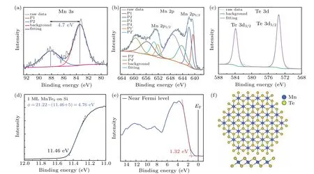
4. Conclusion
猜你喜欢
杂志排行

Chinese Physics B的其它文章
- Modeling the dynamics of firms’technological impact∗
- Sensitivity to external optical feedback of circular-side hexagonal resonator microcavity laser∗
- Controlling chaos and supressing chimeras in a fractional-order discrete phase-locked loop using impulse control∗
- Proton loss of inner radiation belt during geomagnetic storm of 2018 based on CSES satellite observation∗
- Embedding any desired number of coexisting attractors in memristive system∗
- Thermal and mechanical properties and micro-mechanism of SiO2/epoxy nanodielectrics∗