FEM investigation of surface acoustic waves propagating in SiO2/IDT/AlN/Diamond multilayered structure
2021-11-08ZHANGZuweiLIXiaofeiYUANYupengYANGJing
ZHANG Zuwei, LI Xiaofei, YUAN Yupeng, YANG Jing
(Chongqing Acoustic-Optic-Electric Corporation, China Electronic Technology Group Corporation, Chongqing 400060, P.R.China)
Abstract: In this paper, the finite element method(FEM)simulation based on COMSOL software is applied to investigate the SAWs propagating in the SiO2/IDT/AlN/Diamond multilayered structure.The dispersion properties are researched, the conversion of SAW to PSAW is visually presented, and the influences of the Al electrode thickness and SiO2 buffer layer thickness to the SAWs are investigated.At last, a series of SAW resonators based on the SiO2/IDT/AlN/Diamond multilayered structure are fabricated by micromachining, and their frequency responses are detected.The experimental results are found to be mainly consistent with the simulated ones.And the 1st mode SAW in the SiO2/IDT/AlN/Diamond multilayered structure is believed to have the great potential in the further SAW device applications.
Keywords:surface acoustic wave(SAW); FEM simulation; multilayered structure
1 Introduction
Resent years, diamond has attracted great interests because of its highest surface acoustic wave(SAW)velocity among all materials.If a piezoelectric layer, such as Zinc Oxide(ZnO)or Aluminum Nitride(AlN), is prepared on top of the diamond substrate, the multilayered structure is supposed to be the most promising material for the GHz range high frequency SAW devices, which is urgently demanded by the fast growing of information and communication media.AlN films have the highest acoustic wave velocity among all piezoelectric materials, fairly good electromechanical coupling coefficients and temperature stability, excellent mechanical and chemical qualities.So it is seems to be the most attractive candidate for diamond-based high frequency SAW devices[1-3].
However the propagation properties of the SAW in multilayered structures are quite different with that in the monolithic ones.The velocity dispersion and electromechanical coupling coefficient(K2)dispersion must be considered, because of their effects on the inter-digital transducers(IDTs)response.Many efforts have been done to describe the dispersion behaviors of SAWs in the multilayered structures[4-10], such as theoretical studies, finite element modeling(FEM)simulations, or experimental investigations.But most of the research results are formulas and curves, few of them present the visual particle vibrations of different SAW modes at surfaces, geometries and interface.
In this paper, a FEM approach is presented to investigate the SAW dispersion behaviors in multilayered structure.The commercial FEM software COMSOL is used to simulate the first three SAW modes propagating in the AlN films on diamond substrates.The velocity dispersion curves andK2dispersion curves are calculated based on the simulation results.The complex particle vibrations of different wave modes are presented to visually show the conversion of SAW to pseudo SAW(PSAW)in the conditions of varied AlN film thickness.Moreover, the influences of the Aluminum(Al)electrode thickness and Silicon Dioxide(SiO2)buffer layer thickness to the propagation properties of the SAWs are investigated.In order to prove the simulated results, some SAW resonators based on the 1stmode of the multilayered structure are fabricated and their frequency responses are detected.The test results show well coherence with the simulated ones.
2 Modeling
Considering the periodicity of the IDTs of the SAW devices, the propagation property in one periodic unit can represent that in the whole substrate.The simplified 2D FEM model of the SiO2/IDT/AlN/Diamond multilayered structure is established by COMSOL, as seen in Fig.1.The SiO2layer is included because it is usually used as the protection and temperature compensative layer.According to the most commonly used fabrication process,(002)AlN film with c-axis perpendicular to the substrate is selected.The top boundary is set as free, the bottom boundary is set as settled, the left and the right boundaries are set as periodic, and all the inner boundaries are set as continuous.The electric excitation is applied on the Al electrodes.The geometry characters are listed in Tab.1 and the material characters are listed in Tab.2.

Tab.2 Material characters of the FEM model

Fig.1 Simplified 2D FEM model of multilayered structure

Tab.1 Geometry characters of the FEM model
3 Calculations
By using the FEM simulations(modal and harmonic analysis), the frequency response curve of the IDT admittance can be obtained, as shown in Fig.2.The acoustic wave eigenmodes propagating in the multilayered structure can be found out from the admittance curve.The acoustic wave velocity of each eigenmode may be calculated from the poles and zeros of the obtained admittance curve around the resonance frequency.The poles of the admittance are associated with modes for shorted boundary conditions and the zeros with modes for free-circuit boundary conditions on the surface.The electro-mechanical coupling coefficientK2is obtained as:
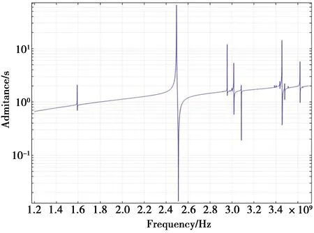
Fig.2 IDT admittance curve of the surface acoustic waves in the multilayered structure
K2=2(vo-vm)/vo,
(1)
wherevois the velocity for free-circuit boundary conditions andvmis the velocity for shorted boundary conditions[6-7].
3.1 Phase velocity dispersion curves of the first three modes
Fig.3 shows the phase velocity(v)dispersion curves of the first three modes in the SiO2/IDT/AlN/Diamond multilayered structure when the thickness of Al electrode layerh1is set to be 0.025λ, the thickness of SiO2layerh2is set to zero, and the thickness of AlN layerhis set to range from 0.025λto 1λ.The curves are plotted as functions of the film thickness ratio(h/λ).The phase velocity of each mode decreases with the increase of the film thickness ratio.

Fig.3 Phase velocity dispersion curves of the first three modes
For the 0thmode, when the thickness ratio is 0.025, the phase velocity is about 9 916 m/s, approaching to the SAW velocity in diamond(vSAW-Diamond≈10 934 m/s)[4].The phase velocity decreases to 5 816 m/s when the thickness ratio increases to 1, approaching to the SAW velocity in AlN(vSAW-AlN≈5 438 m/s)[4].The 0thmode is considered to be Rayleigh wave in the whole thickness ratio range.Its phase velocity is always smaller than the bulk shear wave in the diamond substrate(vS≈12 323 m/s), so no energy leaks into the substrate[3-4].Fig.4a and Fig.4b illustrate the simulated visual particle vibrations of the 0thmode in the conditions ofh/λ=1 andh/λ=0.025 respectively.The intensively elliptical vibrations around the surface which are associated with Rayleigh waves are seen.The vibration shapes hardly change in both the conditions and no strain distribution deep in the substrate is found.This means the 0thmode keeps being Rayleigh wave and no energy leakage exists.The vibration amplitude in the conditions ofh/λ=1 is much larger than that in the conditions ofh/λ=0.025, because the thicker piezoelectric layer can output larger stress and strain.

Fig.4 Particle vibrations of the 0th mode in the conditions of h/λ=1 and h/λ=0.025
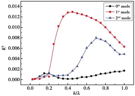
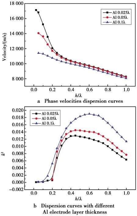
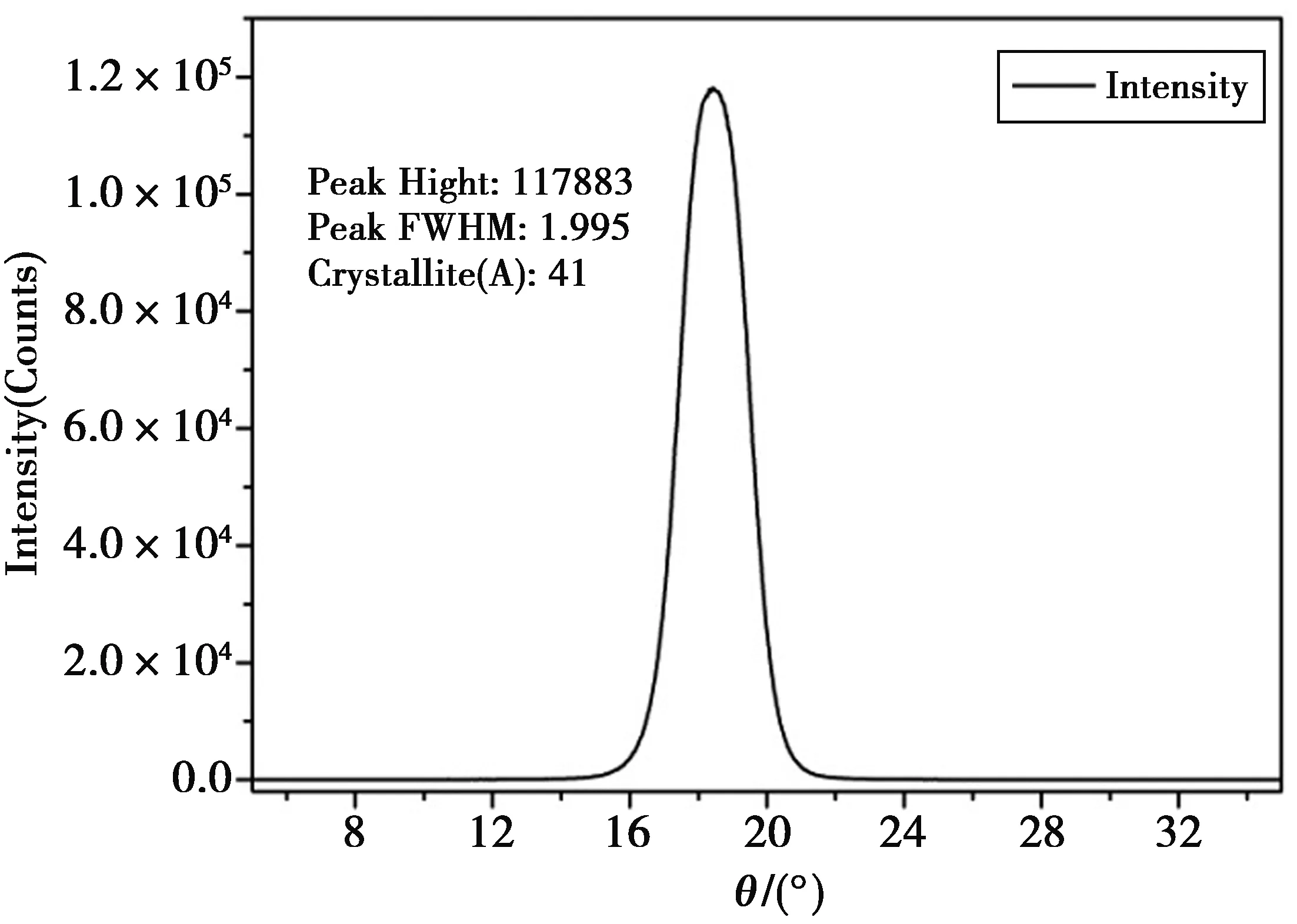
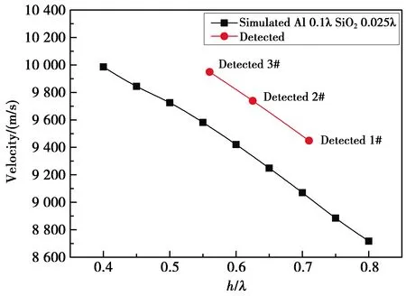
For the 1stmode and the 2ndmode, when the thickness ratio is close to zero, the phase velocities are about 17 120 m/s and 17 028 m/s respectively, approaching to the bulk longitudinal wave velocity in diamond(vL≈18 500 m/s)[4].It is considered that the 1stmode and the 2ndmode are SAWs when the phase velocity is smaller thanvS.But they transform into the PSAWs with the decrease of the thickness ratio and the increase of velocity.To prove this, Fig.5a and Fig.5b illustrate the visual particle vibrations of the 1stmode in the conditions ofh/λ=0.8 andh/λ=0.05, Fig.6a and Fig.6b illustrate the visual particle vibrations of the 2ndmode in the conditions ofh/λ=0.8 andh/λ=0.2.Obviously, in the conditions ofh/λ=0.8 andv Fig.5 Particle vibrations of the 1th mode in the conditions of h/λ=0.8 and h/λ=0.05 Fig.6 Particle vibrations of the 2th mode in the conditions of h/λ=0.8 and h/λ=0.2 TheK2dispersion curves of the first three modes in the SiO2/IDT/AlN/Diamond multilayered structure are shown in Fig.7, when the thickness of Al electrode layerh1is set to be 0.025λ, the thickness of SiO2layerh2is set to zero, and the thickness of AlN layerhis set to range from 0.025λto 1λ.For the 0thmode, when the film thickness ratio increases, theK2increases and shows the first relative maximum value(0.12%)ath/λ=0.15.When the film thickness ratio increases from 0.4 to 1, theK2increases to 0.17%.The 0thmode is considered to be the Rayleigh wave and show very lowK2values in the wholeh/λrange.It is because Rayleigh wave coupling coefficient maximum is exhibited along c-axis[11], but the c-axis of(002)AlN film presented in the model is perpendicular to the substrate. Fig.7 K2 dispersion curves of the first three modes For the 1stmode, theK2keeps in a high level(higher than 1.07%)in theh/λrange from 0.35 to 0.75, and the maximum value of 1.32% is obtained ath/λ=0.45.For the 2ndmode, when the film thickness ratio increases, theK2shows the first relative maximum value(0.12%)ath/λ=0.1 and the second relative maximum value(0.79%)ath/λ=0.7.As a result, the 1stmode is considered to be most usable because of its maximumK2value and broad bandwidth for highK2values.Thus the influences of the Al electrode layer and SiO2layer to the 1stmode will be investigated in the following parts. For the 1stmode, when the thickness of Al electrode layerh1is set to be 0.025λ, a series of phase velocities dispersion curves andK2dispersion curves with different SiO2layer thicknessh2are obtained, as shown in Fig.8a and Fig.8b respectively.It can be seen from Fig.8a thath2hardly affects the phase velocities in theh/λrange from 0.7 to 1, but the phase velocity variation increases with the decrease of theh/λ.When theh/λis close to zero, the velocity of the mode with SiO2layer thickness of 0.1λdecreases to about 11 000 m/s and is much smaller than that with SiO2layer thickness of 0λ.It is because the bulk longitudinal wave velocityvLis slowed down by the SiO2layer.It can be seen from Fig.8b that the maximumK2values slightly increases and shifts to higherh/λwith the increase of the SiO2layer thickness at theh/λrange from 0.4 to 0.8, and the bandwidth for highK2values remarkably narrowed.The relative maximum values at theh/λrange from 0.05 to 0.15, where indicates the PSAW region, is obtained.The relative maximum values increase from zero to 0.23% as the SiO2layer thickness increasing from zero to 0.1λ.So, except for the protection and the temperature compensation, it is believed that the SiO2layer shows few beneficial influences on the usage of the 1stmode in the presented multilayered structure. Fig.8 Phase velocities dispersion curves and K2 dispersion curves with different SiO2 layer thickness For the 1stmode, when the thickness of SiO2electrode layerh2is set to be zero, a series of phase velocities dispersion curves andK2dispersion curves with different Al electrode layer thicknessh1are obtained, as shown in Fig.9a and Fig.9b respectively.It can be seen from Fig.9a thath2hardly affects the phase velocities in theh/λrange from 0.3 to 1, but the phase velocity variation increases with the decrease of theh/λ.When theh/λis close to zero, the velocity of the mode with Al layer thickness of 0.1λdecreases to about 11 500 m/s and is much smaller than that with Al layer thickness of 0.025λ.It is because the bulk longitudinal wave velocityvLis slowed down by the Al layer.It can be seen from Fig.9b that the maximumK2value increases from 1.32% to 1.91% with the increase of the Al layer thickness at theh/λrange from 0.4 to 0.8, where indicates the SAW region, and the bandwidth for highK2values hardly narrowed.In the PSAW region, at theh/λrange from 0.05 to 0.15, the Al layer show few influence on theK2curves.So it is considered that advisably increasing the Al layer thickness can considerably increase theK2values. Fig.9 Phase velocities dispersion curves and K2 dispersion curves with different Al electrode layer thickness As a result, the 1stmode of the SiO2/IDT/AlN/Diamond multilayered structure with the Al electrode layer of 0.1λ, SiO2layer of 0λand the film thickness ratio of 0.6 is believed to have great potential for the SAW device application.Its phase velocity andK2are calculated as 9 420 m/s and 1.91% respectively.To prove the results discussed, some SAW resonators based on the 1stmode are fabricated and detected in the following parts. In order to prove the results discussed above, some SAWresonators based on the 1stmode of the SiO2/IDT/AlN/Diamond multilayered structure are fabricated and their frequency responses are detected.Three types of SAW resonators with different IDTs periods andh/λare selected, as shown in Tab.3.Their electro-mechanical coupling coefficients at these wavelengths are relatively high for the 1stmode according to the simulation. Tab.3 Main structure parameters of the designed SAW resonators A commercial polycrystalline diamond wafer, with the thickness of 400 μm and the surface roughness of 2 nm, is applied as the substrate.The AlN films are prepared by radio frequency(RF)magnetron sputtering, the Al electrodes are prepared by vacuum evaporation depositing, and the SiO2films are prepared by plasma-enhanced chemical vapor depositing(PECVD).The crystallization of the AlN film is investigated by an X-ray diffractometer(XRD, D/max 2500PC).The frequency responses of the SAW resonators are detected by a vector network analyzer(HP 8510). Fig.10 shows the X-ray rocking curve of the RF sputtered AlN film.The peak at about 18.5°of the rocking curve corresponds to the diffraction from the(002)plane of AlN which indicates a perfect perpendicularity of the c-axis to the substrate.The fairly small full width height maximum(FWHM)of 1.995°indicates the high quality of crystallization and piezoelectricity. Fig.10 Rocking curve of the AlN film There are three types of SAW devices are fabricated, which micrographs are shown in Fig 11.Their S21 curves are detected by the vector network analyzer and their impedance curves can be obtained by the transformation of the S21 curves.The resonant frequencyfoand the anti-resonant frequencyfmof each mode can be picked out from the impedance curves.The velocity can be calculated byvo=λ×foand theK2can be calculated byK2=2(fo-fm)/fo.Fig.12 and Fig.13 illustrate the compare of phase velocity andK2between the fabricated devices and the simulated results.It can be seen that their variation trends are consistent with the simulation results.But the detected velocities are larger than the simulation results and the detectedK2are smaller than the simulation results. Fig.11 Micrographs of the fabricated SAW devices on the wafer and the IDTs Fig.12 Compare of the velocities between the simulated results and detected ones Fig.13 Compare of the K2 between the simulated results and detected ones In order to understand the reason for this case, the deice 1# is selected as an example and is annealed in air at 400 ℃ for 2 hours.The frequency responses of the device 1# before and after annealing are shown in Fig.14a and Fig.14b respectively.It is clear that the annealing causes the center frequency downward shift from 3.553 GHz to 3.407 GHz and the peak value shifts from-30.0 dB to-26.3 dB.The velocity shifts from 9 948 m/s to 9 539 m/s, becoming closer to the simulated result(9 394 m/s).Therefore, it is believed that because of the residual stresses produced in the fabrication process of the films the detected velocities are higher that the simulation ones.The thermal annealing relieves the residual stresses by creating defects and dislocations, which result in the reduction of the acoustic velocities[8-9,12].Because of the high velocity of SAW in the Diamond substrate and the AlN thin film, the frequencies of the fabricated SAW resonators reach to about 3.5 GHz, which is much higher than the traditional SAW resonators.But the rough surface of the AlN film causes the degeneration of the insertion loss performance.If some high surface quality piezoelectric film materials, like single crystal lithium niobate film prepared by smart-cut, are used instead of AlN film, the SAW devices based on diamond multilayered structure will performance much lower insertion loss and can be applied in 5G communication. Fig.14 Frequency responses of device 1# before and after annealing In this paper, the FEM simulations are applied to analysis the SAW propagation in the SiO2/IDT/AlN/Diamond multilayered structure.The velocity dispersion curves andK2dispersion curves are calculated based on the simulation results.The complex particle vibrations of different wave modes are presented and visually show the translation of the SAWs to the pseudo SAWs(PSAWs)in the various conditions of AlN film thickness.The influences of the Al electrode thickness and SiO2layer thickness to the propagation properties of the SAWs are investigated.In order to prove the simulated results, some SAW resonators based on the 1stmode of the multilayered structure are fabricated and their frequency responses are detected.The experimental results are mainly consistent with the theoretical ones except the little larger detected velocities induced by the residual stresses produced in the fabrication process of the films.After the thermal annealing, the detected velocities are reduced and the smaller error between the experimental and simulated results is obtained.Therefore, the 1stmode in the SiO2/AlN/Diamond multilayered structure is believed to have great potential in further SAW devices.

3.2 K2 dispersion curves for the first three modes
3.3 The 1st mode propagating in the structure with different SiO2 layer thicknesses

3.4 The 1st mode propagating in the structure with different Al electrode layer thicknesses
4 Experiments

5 Results and discussions


6 Conclusions
