A radar-infrared compatible broadband absorbing surface:Design and analysis*
2021-07-30QingTaoYu余庆陶YuanSongZeng曾元松andGuoJiaMa马国佳
Qing-Tao Yu(余庆陶), Yuan-Song Zeng(曾元松), and Guo-Jia Ma(马国佳)
Aviation Key Laboratory of Science and Technology on Advanced Surface Engineering,
AVIC Manufacturing Technology Institute,Beijing 100024,China
Keywords: stealth,infrared-radar compatible,broadband absorbing,patterned surface
1. Introduction
In modern warfare, aircrafts are subjected to various detection methods. Among them, detection of radar reflection and infrared emission are the two major means to locate and trace an aircraft. The microwave reflected by an aircraft can be collected by radar systems to guide the missile approaching the aircraft. When approaching,an infrared sensor on the missile begins to seek and lock on the infrared signal emitted from the aircraft. To increase aircraft survivability during combats,technologies have been developed to reduce radar reflection in a wide frequency range and to supress infrared emission at the same time.
Radar absorbing materials (RAMs) were developed to mitigate the microwave reflection. RAMs containing ferrites or carbonyl iron flakes (CIFs) are considered to be some of the most effective magnetic absorbents,and have been widely used in stealth coating on aircrafts nowadays. However,a typical CIF composite RAM has a high infrared emissivity[1]between 0.8-1, therefore it becomes an intense infrared source that could radiate large amount of infrared energy at elevated temperature.
Low radar reflection and low infrared emissivity are somewhat contradictory in nature,as low-emissivity materials such as copper, gold, platinum (emissivity below 0.1[2]) and ITO are good conductors and thus are highly reflective to microwave. One of the solutions to infrared-radar compatibility is to apply coating that contains micro aluminum flakes. The sizes of these micro flakes are in order of magnitude smaller than the microwave wavelength, allowing diffraction of the microwave and providing relatively low emissivity at the same time. To ensure low emissivity, aluminum flakes have to be uniformly distributed in the resin, and ideally they should be isolated from each other as aggregation of particles may have a negative influence on radar absorption.
1.1. Patterned surface for stealth application
CIF composite RAMs are high in density, therefore the thickness of such coating on aircrafts is limited to several millimeters and sometimes less than a millimeter. As coating thickness is strictly restricted and the CIF’s permeability is bounded by Snoek’s limit,[3]efforts have been made to creating patterns and structures in RAM coating for broadband radar absorbers.[4-6]Among those attempts, Liet al.[5]increased the-10 dB absorption bandwidth in the range of 2-40 GHz by more than 6 times through engraving periodic square patterns with certain depth on a layer of CIF composite. They conclude that in the low frequency range, the improved performance is dominated by theλ/4 effect inside the engraved gap, while in the high frequency range, diffraction of the electromagnetic waves at structure corners plays a more important role. Similar effects have also been discussed in the biomimic research of Huanget al.,[6]who produced a layer of RAM with hexagonal structures, mimicking the microstructures on the moth eye surface which largely reduces the reflection of visible light to avoid predators. Their results showed that when hexagonal periodic pattern has a side length of 3.2 mm, the-8 dB absorption bandwidth increases from 3 GHz to 11 GHz in the 2-18 GHz range.
On the other hand, frequency selective surfaces (FSSs)are metal surfaces with periodic patterns designed to reflect,transmit or absorb microwave of certain frequencies. Some studies explored the possibility of combining FSS with other materials for broadband radar absorbing purpose. Several articles[7-10]incorporated FSSs between layers of RAMs,forming a sandwich structure which leads to broader absorption bandwidth. Tianet al.[11]combined a top layer FSS with a bottom-layer high resistive surface for infrared-radar compatible stealth purpose. As the FFS periodic pattern of copper film covers more than 80% of the surface area, the resulting surface has an average infrared emissivity below 0.3. However,its radar absorption bandwidth is relatively narrow,where the-10 dB bandwidth merely covers x-band(8-12 GHz). In some of the latest studies,[12-14]two layers of FSSs were combined together to form a broadband absorber. Xuet al.[12]showed that at a thickness of 7 mm and with proper FSS pattern design the-10 dB absorption bandwidth can reach 18 GHz and the infrared emissivity can be maintained below 0.3. Additionally, patterned ITO was used in their study to achieve optical transparency.
In this study, a radar-infrared compatible broadband absorbing surface(RICBAS)design is proposed. The proposed design follows the idea that FSSs play an important role in infrared-radar compatibility. With proper design,an FSS pattern can cover most of the surface area,providing low infrared emissivity and tuning the overall input impedance of the surface at the same time.It couples with patterned CIF composite RAM to promote radar absorbing performance.
A transmission-line-based model (TLM) is developed to analyze the reflection loss of the designed surface and the results are compared with that produced by the finite element method(FEM).Parametric analyses are conducted to explore influences of basic design variables on radar absorbing performance. An optimization is conducted to find the design variables that lead to maximum-10 dB absorption bandwidth within the 2-18 GHz range. An experiment is provided in the end to qualitatively demonstrate that the conceptual design of RICBAS is capable of tuning the reflection loss curve.
2. Design and modeling
2.1. Design
The designed RICBAS combines structured RAM and FSS,as shown in Fig.1.

Fig.1. Schematic of RICBAS structure design: (a)surface structures,(b)a single unit cell.
In the current design, the FSS and the RAM share the same square pattern.This assumption largely reduces the complexity in optimization and manufacturing,yet still allows the study of design principles.
As shown in Fig.1(a),the structure consists of a top layer of thin metal film,a middle layer of CIF composite RAM,and a bottom layer of metal backing. The metal film only covers the top surface of the structures. It is also assumed that the metal film thickness is much larger than the microwave skin depth in the 2-18 GHz range(several hundreds of nanometers for common metals), and much smaller than the microwave wavelength; therefore the thickness effect of the metal film can be neglected. The middle layer has a total thickness oftand the depth of the structure isd. This RICBAS consists of repetitive square unit cells,Fig.1(b),with side length beingaand the side length of the RAM structure can be expressed asac,wherecis between zero and one.
In the analysis,the coating thicknesstis set to be 1.5 mm,which is a typical RAM thickness on an aircraft. The structure depthdshould be strictly smaller thant, as any exposure of the metal backing would drastically increase microwave reflection. The type of the CIF composite used in the current analysis is similar to that in the study of Liet al.[3]Its relative dielectric parameters,shown in Fig.2,are kindly provided by State Key Lab of Advanced Technology for Materials Synthesis and Processing,Wuhan University of Technology.

Fig.2. Relative permittivity and permeability of the CIF composite.
2.2. Modeling
A transmission-line-based model(TLM)is developed for such a patterned surface to analyze the microwave absorbing performance. The result is analyzed and compared with that generated by the finite element method. Parametric analyses are then conducted to study influences of the three primary variablesa,dandcon reflection loss.
The transmission line method has been well studied and widely applied in studying the frequency selective surface[15]as well as RAMs.In the configuration where metal patches are placed on a layer of dielectric, the equivalent circuit is a parallel circuit between impedance of CIF composite RAM and FSS metal film,as shown in Fig.3.

Fig.3. Equivalent circuit of the layered RICBAS surface.
The reflection coefficientΓcan be expressed as
where the air impedanceZair, relative to the free space impedance, is approximately one and the total input impedance of the parallel circuitZincan be written as

In Eq.(2),ZFSSandZRAMare impedances of the FSS top layer and the RAM layer, respectively. In the current design,the RAM consists surface structure with a depth ofd. Therefore, the overall RAM layer may be alternatively considered as a two-layer structure: the lower one is a uniform layer with a thickness oft-d,consisting of only CIF composite;and the upper one is a structured layer of thicknessd, consisting of both CIF and air.
The input impedance of thekth layer in a multi-layer structure[16]can be expressed as

whereλis wavelength.
As the two layers are placed on a metal backing,Z0is 0,and the total input impedance of RAM becomes

whereδcould be either permittivityεor permeabilityμ,andfairis the volume fraction of air.
For FSS surface with square patches, the impedanceZFSSunder normally incident wave can be estimated by the expression[18]

Equations (2), (5) and (8) estimate the overall surface input impedance, which can be tuned by the three geometrical parametersa,candd. Then the overall reflection loss can be estimated using Eq.(1).
3. Model analysis
The reflection loss evaluated by the developed TLM is compared with that generated by a commercial FEM software.In the FEM analysis,a periodic boundary condition is used to study the surface response of microwave by analyzing one single unit cell.
The reflection loss of the uniform slab without patterns is shown in Fig. 4. With the volume fractionfairbeing 0 in Eq. (6) andZin=ZRAM, the result from TLM shows good agreement with that from FEM.The two curves overlap each other, where the maximum discrepancy, as low as 1.6%, occurs at around 8.4 GHz. The resulting curves also agree well with the result by Liet al.[5]

Fig.4.Reflection loss of 1.5 mm uniform slab evaluated by two models.
For patterned surface in the following parametric analysis, a set of nominal values,a=1 mm,d=0.5 mm, andc=0.9,are chosen to set the benchmark. Calculated by both the models,the benchmark reflection loss of the patterned surface with and without the FSS layer(RAM structure only)are given in Fig. 5. In the absence of the FSS layer, as shown in Fig. 5(a), both the models predict an increase of the-10 dB absorption bandwidth, from 4.4 GHz to 6.0 GHz by FEM and to 4.9 GHz by TLM. Also, both the models capture the changing trend that absorption peak moves towards higher frequency.In FEM,the absorption peak appears at 8.0 GHz while the TLM predicts a peak at 7.0 GHz. The intensity of the peak evaluated by FEM is 15.9 dB,4%lower than that of the TLM.The two curves show large discrepancy in the 8-18 GHz range.As discussed by Liet al.,[5]the microwave diffraction at corners of the surface pattern is the dominating mechanism of the reflection loss in high frequency range,which cannot be effectively captured by the current TLM.
Figure 5(b) shows the benchmark reflection loss of the patterned surface with the FSS layer. Compared with the previous results,both the models indicate that the appearance of 1 mm square metal patches on the top surface moves the absorption peak towards lower frequency and reduces the performance in high frequency. The-10 dB absorption bandwidth decreases from 6.0 GHz to 4.7 GHz in FEM,and from 4.9 GHz to 3.9 GHz in TLM.An increase in the intensity of the absorption peak is observed in the FEM result. With the FSS layer,the peak absorption loss increases from-16 dB to-18.3 dB,which could be caused by the overlapping of the absorption peaks of patterned RAM and FSS.

Fig. 5. Benchmark reflection loss: (a) without the FSS layer (RAM structure only), (b) without the FSS layer (RAM structure+FSS pattern).
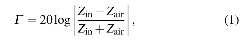
The influence of unit cell sizeais studied first. The results produced by FEM is demonstrated in Fig. 6(a). Whenais 0.1 mm, in an order of magnitude smaller than its nominal value, the absorption peak changes from 6.4 GHz in the benchmark to 8.5 GHz. While the reflection loss between 2-8 GHz decreases,the performance in the range of 8-18 GHz is largely improved.The appearance of FSS in this case has little influence on the curve. In both the cases,the-10 dB absorption bandwidth is larger than that in the benchmark,increasing from 6.0 GHz to 6.7 GHz.
As the side length increases from 0.1 mm to 5 mm,in the case without an FSS layer,the absorption peak moves towards low frequency,but is still higher than that of the uniform slab.A distinct difference is observed in the case with the FSS layer.The 5 mm square metal patch largely affects the reflection loss in the 4-18 GHz range.The absorption peak shifts to 3.2 GHz,and the-10 dB absorption bandwidth drastically decreases to only 0.7 GHz. When the size of the FSS pattern is in the order of wavelength of the microwave, microwaves of higher frequency can not pass the metal patch and thus becomes highly reflective.
The results produced by TLM are given in Fig.6(b). The TLM developed in this study adopts the MG equation to represent the patterned CIF composite layer with a uniform CIF-air layer. The dielectric parameters of such a CIF-air layer only depends on the volume fraction of air,fair,which is independent of the unit cell size. Therefore, the current model does not include the size effect of the RAM structure. Yet, similar trends have been observed with the FSS layer, compared to the results produced by FEM. After comparing the curves produced by the two models, it seems that the FEM model is more sensitive to the variation of unit cell size.
With FEM analysis,it can be shown that further decrease inawill not have much influence on the reflection loss curve.Curves ofabeing 0.05 and below are almost identical to that ofa=0.1. As the size of unit cell is in order of magnitude smaller than the wavelength, the wave does not “see” the individual structure. However,smaller unit cell could affect the infrared emissivity in a negative way. Firstly, ifais smaller than the wavelength of infrared(several micrometers),infrared emittance from the CIF composite may pass through the metal film at the top of the structure. Secondly,if the values ofcandtare kept to be unchanged,smallerawill result in larger overall surface area. Both will increase the total surface infrared energy emission.
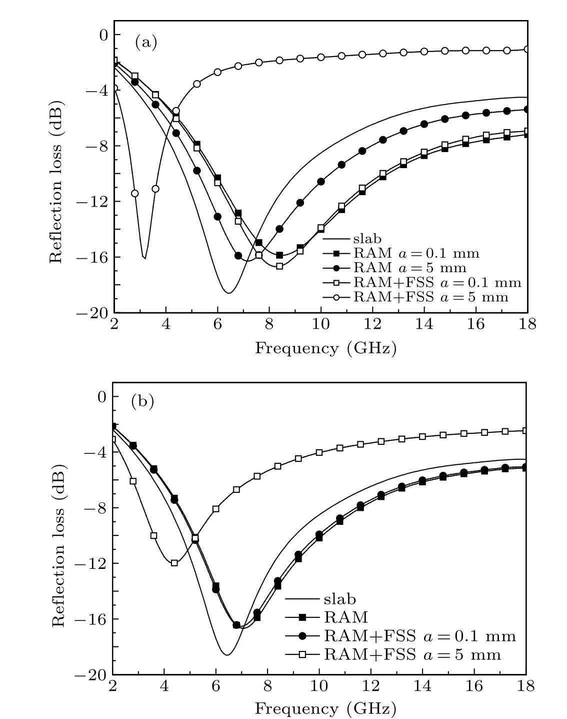
Fig. 6. Influence of the size of unit cell on reflection loss by (a) FEM and(b)TLM.
Influence of the RAM structure depthdhas been discussed by Liet al.,[5]who attributed the improved performance in a high-frequency range to the 4/λresonance at the etched area. Similar trends have been captured by both the models, although the FEM model is more sensitive to the change in structure depth, as the absorption peak in Fig. 7(a)shifts to a higher frequency compared to that evaluated by the TLM model, as shown in Fig. 7(b). Another observation in Fig. 7(a) is that the appearance of 1 mm square FSS layer shifts the two curves differently. The FSS layer has smaller impact to the 0.2 mm depth structure. For example,in the case ofd=1.2 mm, the FSS layer increases the reflection coefficient at 18 GHz from 0.295 (-10.6 dB) to 0.562 (-5.0 dB),while in the case ofd=0.2 mm,such a value increases from 0.562(-5.0 dB)to 0.708(-3.0 dB).This observation implies that the influences on reflection loss by RAM structure and FSS pattern are intertwined,instead of being independent and linear.
In Fig.7(b),it can be seen that,although TLM is capable of capturing trends of the reflection loss with varying structure depth,the resulting curves significantly deviate from the FEM analysis in high-frequency range,and especially under a largedvalue. This could be again caused by the inaccurate representation of structured RAM with uniform CIF-air mixture.Also, the absence of wave diffraction mechanism at structure corners contributes to the error in high frequency.

Fig. 7. Influence of structure depth on reflection loss by (a) FEM and(b)TLM.
The value ofcis the ratio of structure size to the size of unit cella. Withabeing fixed, variation ofcnot only affects the size of the structure (ac), but also affects the CIFair volume fraction (1-c2), thus changing the effective dielectric parameters of the structured layer. In both the FEM and TLM results shown in Figs. 8(a) and 8(b), as the value ofcincreases from 0.8 to 0.95,absorption peaks shift to high frequencies, the-10 dB absorption bandwidth increases and the absorption performance in high frequency is improved. A smallercmeans smaller percentage areal coverage of the metal film, which directly leads to higher surface infrared emissivity. Therefore, the changing trends in Fig. 8 indicate that a trade-off exists between lower infrared emissivity and better radar absorption performance in the presented RICBAS design,where an optimization can be used to find a balance point between the two sides.

Fig.8. Influence of the value of c on reflection loss by(a)FEM and(b)TLM.
4. Optimization
The above parametric analyses have shown that the three variables affect the overall radar absorbing performance in a convoluted way. Both RAM structure and FSS pattern can be used to tune the reflection loss curve. An optimization is conducted in this section aiming at maximizing the-10 dB absorption bandwidth in the 2-18 GHz range.
On the other hand, as RICBAS is also designed for infrared stealth, a low infrared emissivity, say 0.3, is set as a boundary condition in the optimization process. The average infrared emissivityεavgof the patterned surface may be estimated by the empirical formula[11]

The value ofdis bounded by the thickness of the CIFcomposite RAM layer,so 0<d <1.5 mm. Based on the parametric analysis ofa,if the size of FSS pattern is large,it will hinder the radar absorption in high frequency range.Additionally,when the size ofais close to 0.1 mm,it will pose almost negligible effect on radar absorption. Therefore,ais set to be 0.1≤a ≤3 mm to narrow down the optimization search space.

Fig. 9. Curve of reflection loss optimized for maximum -10 dB absorption bandwidth.
The optimization process is performed by the embedded optimizer of the commercial FEM software. After several dozens of iterations, a set of optimized values are given asa=0.58 mm,d=1.08 mm andc=0.87. The resulting curve of reflection loss at the optimized points is plotted along with that of the uniform slab in Fig.9. The optimized design yield-10dB reflection loss between 7.9 GHz and 18 GHz. The corresponding absorption bandwidth is 10.1 GHz,115%more than that of the uniform slab the absorption peak occurs at 11.4 GHz with a maximum-22.5 dB reflection loss. The corresponding surface infrared emissivity,according to Eq.(12),would be around 0.287. In the current design,FSS shares the same pattern with the RAM structure. This design can be rather easily realized by first depositing a layer of metal on the CIF composite by physical vapor deposition (PVD), and then manufacturing the pattern and structure with machining or laser. Although the design reduces the difficulties in design and manufacture,it also limits further optimization. In future research, FSS and RAM may have independent patterns, and the optimized results may yield a better infrared-radar stealth performance.
5. Experiment
An experiment was conducted to demonstrate that the conceptual design is capable of improving the radar absorption performance while allowing most of the surface being covered by metal film.
5.1. Experiment procedure
To prepare the CIF composite layer, CIF was fully mixed with epoxy resin and uniformly sprayed onto two 180 mm×180 mm steel plates. They were then placed in an oven to cure for 12 hours at 50°C.The resulting CIF composite RAM is a 1.4-mm-thick black layer as shown in Fig.10(a).A vector network analyzer was used to measure the reflection loss curve of one plate. After that,both plates were placed in a vacuum chamber and a layer of copper was deposited on the RAM surface by magnetron sputtering, a type of PVD process. The fully coated surfaces have a purplish-orange color with metallic gloss, as shown in Fig. 10(b), and its reflection loss was measured once again.

Fig.10. (a)CIF composite slab and(b)copper coated CIF composite slab.
Structures were constructed on the surfaces with an ultrafast laser which uses picosecond or femtosecond laser pulse to remove materials with minimum thermal effect and high precision. This minimizes the degradation of the CIF material under high temperature. However,the downside is that the ablated material can be trapped in the small gap,which prevents further ablation in the depth. After several attempts, it seems that the maximum structure depth under reasonable processing time would be around 0.5 mm. Therefore,two sets of surface structures(1)a=1.5 mm,d=0.5 mm,c=0.9 and(2)a=1.0 mm,d=0.5 mm,c=0.9 were separately constructed on the two surfaces,as shown in Figs.11(a)and 11(b). An optical microscope with large depth-of-field capability was used to measure the geometries of the manufactured structures, as shown in Figs.11(c)and 11(d). Finally,the reflection loss of the structured surfaces was measured at the end.

Fig.11.(a)and(c)Pictures of 1.5 mm unit cell sample and its geometry measurement. (b) and (d) Pictures of 1.0 mm unit cell sample and its geometry measurement.
5.2. Result and discussion
The three reflection loss curves are shown in Fig. 12.The curve of the the CIF composite slab has a peak value of-17.5 dB at 6.08 GHz,and the-10 dB absorption bandwidth is 3.8 GHz. After the surface was covered by copper film,the reflection loss is around 0 dB,indicating that microwaves was fully reflected.

Fig.12. Reflection loss curves of different surface structure and treatment.
As structures were manufactured on the surface, microwaves can once again enter the CIF composite. When the size of unit cell is 1.5 mm, the absorption peak moves to 5.52 GHz and the intensity of the peak increases to-19.4 dB.However, the high frequency performance is impaired and the-10 dB absorption bandwidth is decreased to 3.12 GHz,which is probably due to the lack of structure depth and large FSS pattern size as discussed previously. Since the structure depth is difficult to further increase, the size of unit cell is set to be 1.0 mm in the second set of parameters. As shown in Fig. 12, whena=1.0 mm the absorption peak shifts to a higher frequency at 6.92 GHz with a peak value-16.7 dB.While the low frequency performance is affected,the high frequency performance is comparable to that of the CIF composite slab. The-10 dB absorption bandwidth is broadened by 8.1%,to 4.12 GHz.
The above experiment only serves as a demonstration.It shows that surface structure can be used to tune the radar absorption performance,increasing the absorption bandwidth when the surface is mostly covered by low-emissivity metal film. It also shows that some changing trends can be captured by the model.
More systematic experiments are required in the future to verify this conceptual design. Nevertheless, many obstacles are on its way to practical application. In the presented experiment,copper was used as the low emissivity material,[2]which is prone to be oxidized under elevated temperature, causing significantly higher emissivity. Although noble metals such as gold and platinum could maintain low emissivity at high temperature,particle erosion under flight conditions could remove the soft metals in a short time. This may require hard and infrared transparent film on the top to protect the noble metals. Also,the size of applied workpiece is limited by vacuum chamber size of PVD equipment. Manufacturing patches or using other metal spraying technology could be practical approaches to this problem. Also, more comprehensive experiments are required to ensure that base material properties are unaffected during the process. In the presented experiment, we took more than 3 hours to manufacture structures on a 180×180 mm surface using ultrafast laser technology.One solution for large-scale production could be imprinting the CIF composite using metal mold before the resin is fully cured.Metal deposition with mask could replace the laser processing in constructing FSS pattern.
6. Conclusions
A radar-infrared stealth surface has been designed. Its radar-infrared compatibility and broadband radar absorption are achieved by means of surface patterning. The RAM structure and the FSS pattern govern the surface radar absorption.Influences of structure and pattern geometries on reflection loss are studied by a developed transmission-line-based model along with finite element analysis. They are summarized as follows:
(1)The developed TLM is capable of capturing variations in radar absorbing performance qualitatively. The omission of diffraction mechanism and the inaccurate representation of the structured layer lead to large deviation from the FEM results especially in high frequency range.
(2) Decrease in pattern size, increase in structure depth and decrease in ratio of pattern size to unit cell size lead to improved reflection loss in high frequency range and reduced performance in low frequency range.The absorption peak also shifts to a higher frequency.
(3)Increased pattern size can significant reduce the reflection loss in high frequency, as the FSS layer becomes more reflective to high frequency microwave. An intense absorption peak may be found at a low frequency,which means that proper FSS could be used to improve the reflection loss in low frequency.
Optimization was conducted to maximize the-10 dB absorption bandwidth. An optimized solution is found near the pointa=0.58 mm,d=1.08 mm andc=0.87, which leads to a 10.1 GHz absorption bandwidth, more than two times of the unstructured RAM. An experiment is conducted to determine the capability of structure design in tuning the overall radar-infrared compatibility.
杂志排行

Chinese Physics B的其它文章
- Numerical simulations of partial elements excitation for hemispherical high-intensity focused ultrasound phased transducer*
- Magnetic-resonance image segmentation based on improved variable weight multi-resolution Markov random field in undecimated complex wavelet domain*
- Structure-based simulations complemented by conventional all-atom simulations to provide new insights into the folding dynamics of human telomeric G-quadruplex*
- Dual-wavelength ultraviolet photodetector based on vertical(Al,Ga)N nanowires and graphene*
- Phase-and spin-dependent manipulation of leakage of Majorana mode into double quantum dot*
- Deep-ultraviolet and visible dual-band photodetectors by integrating Chlorin e6 with Ga2O3