Strain-tunable electronic and optical properties of h-BN/BC3 heterostructure with enhanced electron mobility*
2021-07-30ZhaoYongJiao焦照勇YiRanWang王怡然YongLiangGuo郭永亮andShuHongMa马淑红
Zhao-Yong Jiao(焦照勇) Yi-Ran Wang(王怡然) Yong-Liang Guo(郭永亮) and Shu-Hong Ma(马淑红)
1School of Physics,Henan Normal University,Xinxiang 453007,China
2School of Science,Henan Institute of Technology,Xinxiang 453003,China
Keywords: heterostructure,electronic and optical properties,first-principles calculation
1. Introduction
Since the advent of graphene, atomically thin twodimensional(2D)layered materials,such as insulating hexagonal boron nitride (h-BN), semiconducting molybdenum disulfide (MoS2), and conducting MXenes, have triggered world interest due to their superior properties[1,2]and the possibility of combining diverse atomic layers to create mechanically stacked heterostructures for manufacturing highperformance devices.[3-9]
Owing to the atomically flat and inert surface, h-BN monolayer has proven to be beneficial to a variety of multifunctional devices consisting of graphene,[10-13]MoS2,[14-17]and others.[18-20]For example, the use of h-BN thin film as a substrate for monolayer MoS2can reduce the Coulombic charge scattering, lower the Schottky barrier height, and enhance the carrier mobility, showing excellent performance for optoelectronic device.[5,14,17,21]This has also been evidenced on another Gr/h-BN/MoSe2heterostructure by vertically stacking graphene (Gr) on the top of 2D h-BN and MoSe2.[3,22]
Likewise, the semiconducting BC3monolayer, mimicking graphene in geometrical structure, has shown distinctive features such as a high elastic moduli (~256 N/m), an excellent thermal conductivity (~410 W/mK), a relatively high carrier mobility of hole (5.13×104cm2·V-1·s-1along the armchair direction), a favorable optical response to visible light,[23,24]and a strain-tunable electronic and optical properties,[23-26]improved optical responses via combining with C3N monolayer forming heterostructure,[27]which make it appealing to optoelectronic device design. Besides, the controllable properties via using an electric-field/strain have been predicted in a number of other van der Waals (vdW)heterostructures.[4,27-30]
It is thus intriguing to make clear what the properties of the heterostructure vertically stacked by BC3and h-BN monolayers are,and how the heterostructure responds to an applied external electric field and strain. In this work, we study the feasibility of forming 2D heterostructure of h-BN/BC3,focusing on its stability,mechanical property,carrier mobility,electronic and optical properties, by performing first-principles calculation. Moreover, the electronic band structure of h-BN/BC3is evaluated under an applied electric field and external strain,and the optical properties are investigated as well.
2. Computational details
First-principles calculation was performed within the density functional theory (DFT) framework by using projector-augmented wave (PAW) pseudopotential, as implemented in VASP code,[31]in conjunction with the generalized gradient approximation (GGA) of the Perdew-Burke-Ernzerhof(PBE)functional.[32]A plane wave basis set with a kinetic energy cutoff of 500 eV and the van der Waals(vdW)interaction with the DFT-D2 correction[33]were considered in the calculations. The optimized structures were obtained by relaxing all atomic positions through using the conjugate gradient scheme until the energy and force converged to 10-5eV and 0.01 eV/˚A,respectively.
The optimized lattice parameters of freestanding h-BN and BC3monolayer were 2.51 ˚A and 5.17 ˚A, respectively,which together with the interatomic bond lengths are shown in Fig. 1(a). Figure 1(a) also shows the comparison between our results and previous results in the literature.[22,25]The unit cell of the h-BN/BC3heterostructure with a small lattice mismatch of about 2.9%, was prepared with different stacking patterns by using a 2×2 supercell of h-BN monolayer and a primitive cell of BC3monolayer(see Figs.1(b)-1(e)),consisting of six boron atoms, six carbon atoms, and four nitrogen atoms,and a vacuum layer of 16 ˚A.The Brillouin zone[34]was sampled with 7×7×1 and 11×11×1k-points for structural relaxation and electronic property calculations, respectively,and the charge transfers were obtained by the Bader charge method.[35]
3. Results and discussion
3.1. Equilibrium geometrical structure and stability


Fig.1. (a)Top views of h-BN and BC3 primitive unit cells with their lattice parameters(a1,a2)and(b1,b2),and hexagonal Brillouin zone and three high-symmetry points, Γ, M, and K in reciprocal space with basis vectors g1 and g2. (b)-(e)) Top and side views for optimized configurations of h-BN/BC3 heterostructure. Corresponding bond distances,interlayer distances,and formation energies are also shown.
Meanwhile, the most favorable configuration S1is also determined by the increased energy(ΔE)relative to the equilibrium configuration of h-BN/BC3as indicated in Fig. 2(a),which are obtained by examining the lateral displacements of the h-BN monolayer along the in-planexandydirections (δxy) in the h-BN/BC3interface, respectively. In the case of configuration S1, the binding energy (Ebind) defined byEbind= (Etotalh-BN-Etotalh-BN+BC3)/S, whereEtotalh-BN+BC3denotes the sum of the total energy of freestanding h-BN and BC3monolayer fixed in their corresponding heterostructure lattice,Sis the sectional area of h-BN/BC3, theEbindis estimated to be-22.04 meV/˚A2,quite close to the C3N/graphene(-20.72 meV/˚A2).[36]Besides,the excellent structural stability of configuration S1is shown in Fig. 2(b) by varying its binding energy with vertical interlayer spacing (d) between the h-BN sheet and BC3sheet. In the equilibrium geometry,the vertical interlayer distanced=3.15 ˚A implies the absence of chemical bonds between the h-BN and BC3sheets, thus confirming the vdW interaction at the h-BN/BC3interface.
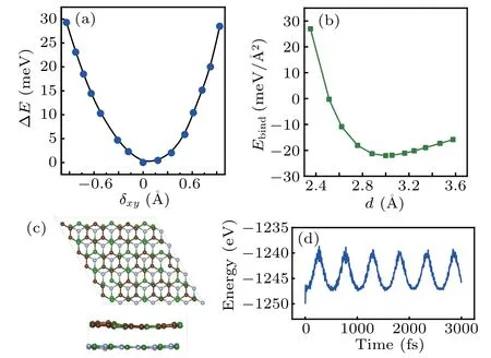
Fig.2. (a)Evolution of total energy difference with displacement δxy of the BC3 layer relative to h-BN, with origin taken at the lowest energy confgiuration. (b) Binding energy per unit cell versus interlayer spacing d of h-BN/BC3 heterostructure. [(c),(d)]Molecular dynamics simulations for fnial structural confgiuration after 3000 fs and total energy fluctuations with time for h-BN/BC3 at T =300 K,respectively.
Additionally,the good thermal stability of h-BN/BC3heterostructure at 300 K is verified by the slight energy fluctuation in a period of 3 ps in time steps of 1 fs and the well-retained final structure shown in Figs. 2(c) and 2(d), obtained by performing theab initiomolecular dynamics (AIMD) simulations with the constant particle number-volume-temperature(NVT)canonical ensemble.[37]All the features manifest a stable equilibrium geometry of configuration S1 for the vdW h-BN/BC3heterostructure.
3.2. Mechanical properties
According to the calculations in Table 1,the four independent elastic constants:C11,C22,C12, andC44(1.18 N/m)and the others fit well with Born’s mechanical stability criteria:[41]C44>0,C11>|C12|, and (C11+2C22)C33>2C213, displaying a good mechanical stability of the h-BN/BC3heterostructure. Moreover,the nearly identical elastic constants(C11(22)),the Young’s moduli, and the Poisson’s ratios along different directions show an isotropic behavior of the h-BN/BC3heterostructure, as well as similar compressibility, stretchability to its components due to the quite similar elastic constants. In contrast, the stiffness of the h-BN/BC3nanohybrid is greatly improved by nearly twice larger in elastic constants(C11=583.454 N/m andC22=580.59 N/m)and the Young’s moduli than its two isolated components. In comparison with the C3N/graphene heterostructure,[36]the h-BN/BC3is predicted to have a slightly less stiffness and a quite close Poisson’s ratio.
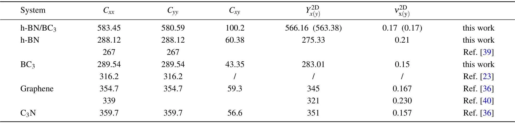
Table 1. Calculated elastic constants Cxx(yy/xy) (N/m)(x=1,y=2),Young’s modulus Y2D x(y) (N/m),and Poisson’s ratio ν2Dx(y) for h-BN/BC3 nanohybrid in comparison with those of monolayer h-BN,BC3 and graphene.
3.3. Electronic properties
To gain more knowledge of the h-BN/BC3heterostructure,we calculate the electronic properties such as the electrostatic potential, electron charge redistribution and electronic band alignment. As shown in Fig. 3(a), the electrostaticpotential-well depths of its two isolated components are almost identical, giving rise to a rather weak electron charge redistribution occurring in the vdW gap.This is in good accordance with the plot of the three-dimensional(3D)charge density difference (CDD) and plot of thexy-plane average CDDversus zshown in Fig.3(b). A small number of 0.02 electrons are predicted to flow from h-BN side to BC3sheet. It is notable that all the band structures are calculated at GGA-PBE level and the obtained band-gaps are 4.65 eV and 0.67 eV for the freestanding h-BN and BC3sheet,respectively,which are in good agreement with other calculations.[27]In Fig.3(c),the projected band structures on h-BN(black dots)and BC3(red dots) monolayer display that the electronic states of h-BN in the h-BN/BC3composite are far from the Fermi level and that the electronic states of BC3monolayer are preserved as well as those of single-layer BC3. In other words,neither the conduction band minimum (CBM) nor the valence band maximum(VBM) of h-BN/BC3is disturbed by h-BN. The band-gap of h-BN/BC3gets narrower slightly down to 0.56 eV at PBE level(1.70 eV at HSE06 level) relative to that of monolayer BC3(0.67 eV at PBE level). Like h-BN/InSe,[42]the h-BN/BC3heterojunction exhibits type-I band alignment (see Fig. 3(d))due to the large band-gap discrepancy between the h-BN and BC3, which is useful for light-emitting diodes (LEDs) and optoelectronic devices requiring a quantum well structure.Meanwhile,the work function(Φ)defined byΦ=Evac-EF,withEvacandEFdenoting the vacuum level and Fermi level,respectively, is obtained to be 5.21 eV for h-BN/BC3, which is between those of monolayer h-BN (6.19 eV) and monolayer BC3(4.85 eV). All these characteristics show a weaker vdW interaction on forming the h-BN/BC3heterostructure and its electronic structure is mainly predominated by monolayer BC3.
Further considering a heterostructure as an electronic device, we evaluate the electronic band structure of h-BN/BC3heterostructure under external electric field (E-field). As shown in Fig. 4, the appliedE-field has a slight effect on the electronic band structure, which retains an indirect semiconducting band. For instance,the tiny upshift(less than 0.1 eV)of the conductive band minimum, combining with a nearly constant valence band maximum, gives rise to the band-gap ranging from 0.51 eV to 0.61 eV under anE-field. What is notable is that the valence band edge atKpoint moves downward with the positiveE-field increasing,while under the action of a negativeE-field it shifts to higher energy and this upshift becomes more prominent withE-field turns more negative,finally the VBM moves away fromΓto K point under anE-field strength of-0.5 V/˚A,quite approaching to the Fermi level (EF). Meanwhile, the further increasing of negativeEfield strength can narrow the band-gap to 0.28 eV under anEfield strength of-0.7 V/˚A,by downshifting the CBM.Overall,the electronic band structure of h-BN/BC3heterostructure exhibits a slight variation under the appliedE-field with its strength less than 0.5 V/˚A.
Fig. 3. (a) Average electrostatic potential of h-BN/BC3 heterostructure versus z. (b) Planar average charge density difference (CDD) versus z of heterostructure,with insert showing 3D isosurface of CDD and the cyan/yellow region representing electron depletion/accumulation with an isosurface value of 0.0004 e/˚A3. (c)Band structures(at PBE level)of monolayer h-BN,monolayer BC3, and h-BN/BC3 heterostructures, with Fermi level(EF)set to be zero. Contributions of BC3 and h-BN to the projected band structure are represented in red and black, respectively. (d) Band alignments of monolayer h-BN,monolayer BC3,and h-BN/BC3 heterostructures with respect to the vacuum level.
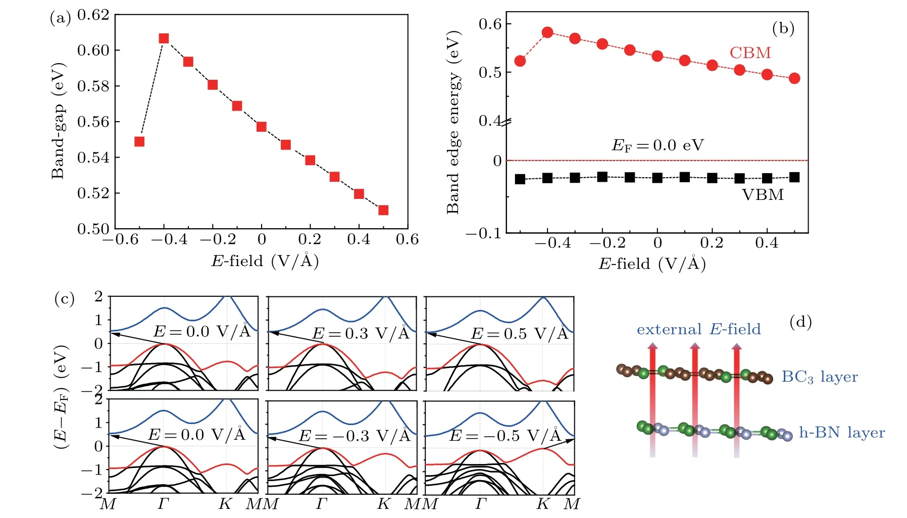
Fig.4. Variation of(a)band-gap,(b)band-edge,and(c)electronic band structures of h-BN/BC3 heterostructure with external electric fields(E-field).(d)EF being set to be zero and applied E-field being defined,with the arrow indicating the forward direction.
3.4. In-plane strain effect on heterostructure
3.4.1. Carrier mobility under uniaxial strains

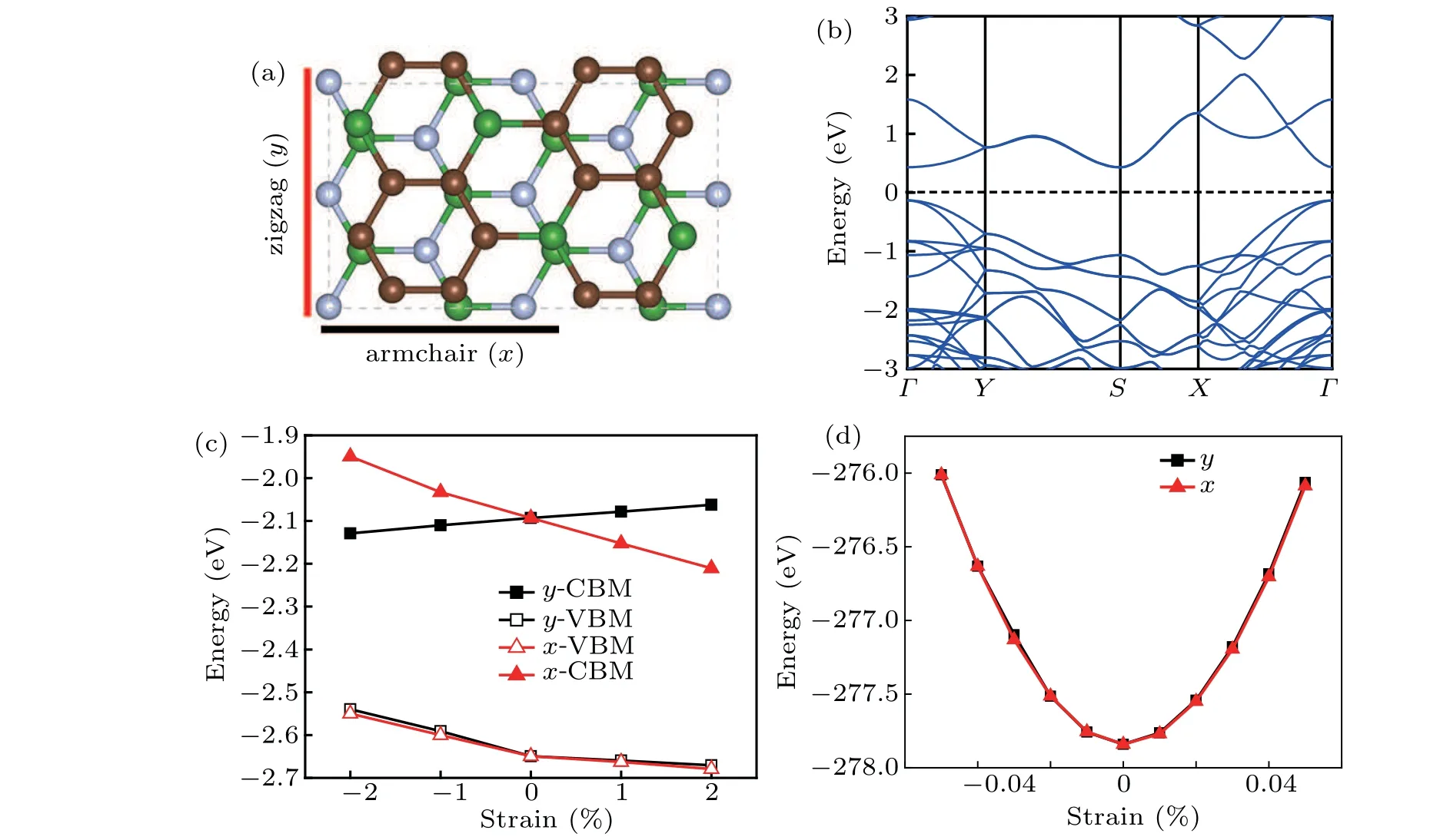
Fig. 5. (a) Orthogonal supercell of h-BN/BC3 heterostructure, (b) band structure of h-BN/BC3 heterostructure, (c) band energies of the VBMs and CBMs versus uniaxial strain along armchair and zigzag direction for h-BN/BC3,and(d)total energy with respect to uniaxial strain relationship along x direction and y direction of h-BN/BC3.

As displayed in Fig. 5(a), the orthogonal supercell of h-BN/BC3is used to calculate the carrier mobilities along thexdirection andydirection, and the related results are given in Table 2. Firstly, the effective mass in h-BN/BC3is predicted to be 0.18mefor electrons and 0.90mefor holes along thexdirection,1.68mefor electrons and 0.72mefor holes along theydirection in our studies. As for other two elements related to the carrier mobility, the DP constantE1is a parameter of the coupling strength of electron or hole to the acoustic phonon,which can be calculated by linearly fitting the data of compressing and stretching the lattice constants along thexdirection andydirection in Fig.5(d).Meanwhile,the mobile carries of monolayer BC3are listed in Table 2,which have a slight difference with previous calculations,[26]the possibility may be the PBE functional considered in our calculation while HSE06 functional employed in the work of Zhanget al. It can be seen that the calculated values ofE1along thex/ydirection for hole/electron in Table 2 for h-BN/BC3are different from those for the monolayer BC3.In particular,for the h-BN/BC3the absolute value ofE1along thexdirection for electron is nearly doubled and inversely, that of hole along the same direction is considerably lowered to 0.80. And the elastic modulusCis estimated at 583.45 N/m and 580.59 N/m along thexdirection andydirection for h-BN/BC3, nearly twice as much as that of monolayer BC3.[26]Comparing with BC3monolayer,the enhanced mobile carries in h-BN/BC3correspond to the narrower band-gap.

Table 2. Calculated deformation potential constant E1,in-plane stiffness C,effective mass m*,and electron and hole mobility μ in x direction and y direction of h-BN/BC3 heterostructure at 300 K.
Based on the above calculations, the carrier mobilities of h-BN/BC3at room temperature (300 K) are given in Table 2, which shows an anisotropic behavior and is nearly ten times larger than that of monolayer BC3, except for the lowered hole mobility along thexdirection. The obtained mobility for electrons is 4.86×103cm2·V-1·s-1and 1.07×103cm2·V-1·s-1along thexdirection andydirection, respectively, while that for holes along thexdirection goes up to 16.09×103cm2·V-1·s-1, twice as large as that along theydirection. The enhanced carrier mobility is quite vital for high-performance optoelectronic devices.
3.4.2. Electronic and optical properties under biaxial strains
A number of previous theoretical and experiment research studies show that the use of external strain is an effective method to modulate the electronic and optical properties of the 2D materials.[25,46]Hence, we also examine the effect of in-plane biaxial strain (ε‖) ranging from-6% to 6% as proposed previously[25]on the electronic and optical properties of h-BN/BC3,with the definitionε‖=(l-l0)/l0,withlandl0corresponding to the lattice constant with and without strain.At zero strain,a band-gap of 1.70 eV obtained at HSE06 level enable the h-BN/BC3heterostructure to be a promising photocatalyst with a visible-light absorption. Like the bilayer BC3,[25]an external strain is used to modify the electronic band structure of h-BN/BC3,i.e., band-gap expands with the tensile strain increasing due to an upshift of CBM at a high symmetryMpoint together with the almost unchanged VBM atΓpoint, and an inverse case under the compressive strains as shown in Fig. 6(a). A nearly linear increase of the bandgap with strain varying from-6% to 6% is observed from Fig. 6(b), except for a slight deviation under a compressive strain of 4%. Thus, it is feasible to moderately modulate the band gap of h-BN/BC3via applying an external strain. To evaluate the thermal stability,ab initiomolecular dynamics(AIMD) simulations are conducted for h-BN/BC3under 6%and-6%strains at 300 K.Figure 7 shows that the energy oscillates within a small range for h-BN/BC3during the period of AIMD simulation,and the final relaxed configuration has a slight deformation compared with the initial structure. Hence,it is confirmed that the h-BN/BC3possesses good stability under strain.
The optical absorption properties are further evaluated by the complex dielectric functionε(ω)=ε1(ω)+iε2(ω). The imaginary partε2(ω)is obtained from the electronic structures by using the joint density of states and the optical matrix overlap,and the real partε1(ω)follows the Kramers-Kroning relationship. The obtained dielectric constants (see Fig. 6(c))show an optical gap of 2.05 eV for h-BN/BC3, confirming the visible-light absorption. Meanwhile, one can observe an enhanced intensity of peak and a prominent red shift in the imaginary part of dielectric function spectrum for h-BN/BC3under zero strain as compared with those for BC3monolayer.Especially, there are two absorption regions for h-BN/BC3,i.e., the high absorption region from 1.5 eV to 5.0 eV, and the low absorption region between 5.0 eV and 10.0 eV. The large area under theε2curve in the visible-light region from 1.5 eV to 5.0 eV with the highest peak of absorption spectrum at 2.73 eV, implies a high efficiency visible-light absorption and high absorption coefficient at these frequencies for h-BN/BC3. Additionally, under an applied tensile strain this heterostructure shows an optical response quite similar to pristine h-BN/BC3. In contrast, the applying of compressive strain(i.e.,-6%)can redshift the optical spectrum,with bandgap reducing 0.68 eV, and the peak intensity lowering about 3.80 eV.
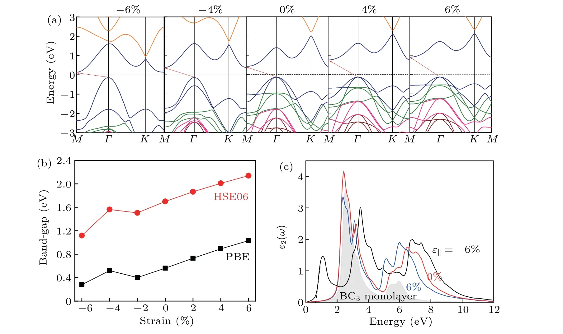
Fig. 6. Calculated results for h-BN/BC3 heterostructure under applied in-plane biaxial strain (ε‖). (a) Electronic band structure (at PBE level), (b)band-gap(at PBE/HSE06 level),and(c)imaginary part of dielectric function.

Fig.7. Variations of energy with AIMD simulation time for h-BN/BC3 heterostructure under 6%and-6%strains with simulation lasting 5 ps at 300 K.And resulting structure is in the middle of the image.
4. Conclusions
By using first-principles calculation, we have studied the structural, mechanical and electronic properties of the h-BN/BC3heterostructure. The results indicate that the electronic properties of BC3monolayer are well preserved and the electron mobilities are enhanced by around ten times in the ultrahigh stiff van der Waals heterostructure. Moreover,the applying of an external electric field only induces its electronic band structure to be modified slightly, while an applied external strain can manipulate the electronic and optical properties of h-BN/BC3,especially under compressive strain. These findings manifest that the h-BN/BC3heterostructure can be used in BC3-based optoelectronic devices.
杂志排行

Chinese Physics B的其它文章
- Numerical simulations of partial elements excitation for hemispherical high-intensity focused ultrasound phased transducer*
- Magnetic-resonance image segmentation based on improved variable weight multi-resolution Markov random field in undecimated complex wavelet domain*
- Structure-based simulations complemented by conventional all-atom simulations to provide new insights into the folding dynamics of human telomeric G-quadruplex*
- Dual-wavelength ultraviolet photodetector based on vertical(Al,Ga)N nanowires and graphene*
- Phase-and spin-dependent manipulation of leakage of Majorana mode into double quantum dot*
- Deep-ultraviolet and visible dual-band photodetectors by integrating Chlorin e6 with Ga2O3