Design of Assembled PCB Imaging System Based on Laser Triangulation
2021-07-14LIUQingfengLIBoWANGQiZHAOShengANWanqingSUXinmingLIUXiaoningZHUXi
LIU Qingfeng ,LI Bo ,WANG Qi ,ZHAO Sheng ,AN Wanqing ,SU Xinming ,LIU Xiaoning,ZHU Xi
1 School of Astronautics,Harbin Institute of Technology,Harbin 150001 2 Beijing Institute of Spacecraft Environment Engineering,Beijing 100094
Abstract:With the increasing miniaturisation and integration of electronic products and the increase of heat,it is necessary to design and introduce heat sinks and install fans.The volume of electronic components,especially the height,is very important for the structural and thermal design of electronic devices.This paper presents a design scheme of an online height measurement device based on laser triangulation and commercial charge coupled device(CCD).It analyzes the principles of electronic component height measurement,and expounds the composition and working principle of the laser measurement system.In addition,the commonly used methods to determine the center position are compared and analysed.These methods include circle fitting,gray centroid and extension method or Gaussian fitting.These methods usually lead to different results.The experimental results show that the fitting speed of the gray centroid is faster.The 3D model of components is given through measurement,and the error factors affecting measurement are analysed.
Key words:laser triangulation,electronic component height,assembled PCB
1 INTRODUCTION
With the increasing demand for miniaturisation of electronic products and equipment,people are paying more attention to the research of component heat dissipation design.The heat dissipation of components is related to the service life of electronic products,long-time uninterrupted work,the volume of components,especially the height,therefore the structural heat dissipation design of electronic equipment is very important for manufacturers.In the main design stage,or finished product design stage of an electronic product,how to quickly and economically detect the height of assembled components is an urgent task to solve.
Automatic optical inspection (AOI)is a fast developing new testing technology.Based on the optical principle of detection,AOI equipment uses high-speed and high-precision visual processing technology to automatically detect various installation errors and soldering defects after electrical assembly of the printed circuit board (PCB) from a fine spacing high-density board to a low-density large-size board on the production line,such as abnormal seating of components and incorrect installation height caused by pin false soldering.AOI equipment can easily provide online inspection solutions to improve production efficiency and welding quality.Many manufacturers use AOI test equipment,but the general AOI measurement results do not have information about the height of a single PCB component.AOI equipment with high measurement capability is very expensive,and so is a 3D measurement instrument.In contrast,2D imaging commercial charge coupled device (CCD) is a mature market-oriented product (open source),which derives the central position information of the equipment from the PCB design blueprint.A laser triangulation system is used to measure the height of the tested circuit components and the position of the PCB,and a 3D model is derived from the height information based upon data interpolated at the software level with the 3D model of the heat dissipation structure to avoid the contact and interference between the components and the heat dissipation structure in space.
Since the devices with large heat dissipation on the PCB of the product need a heat sink design,the compact installation space will affect the heat dissipation capacity of each prominent structure.Therefore,it is necessary to check whether the safety distance between PCB components and heat dissipation structure meets the design requirements.The parameters provided in the chip data sheet are inaccurate,because the chip data sheet has a tolerance range of 0.5 mm for the outline packaging of components,while the chips of different batches may be even be more different.This is the reason why we design PCB component using a height measuring device.
1.1 Laser Triangulation Method
Compared with other non-contact measurement methods,such as height calliper,high-performance laser triangulation method,the laser triangulation method has many advantages,including avoiding contact with the measured object,wide measurement range,large offset distance,good stability,simple and accurate measurement,small volume,convenient installation,small environmental impact,and convenient automatic online detection.In this paper,a PCB component height measurement system was designed including 1D laser triangular displacement meter,2D displacement table and host computer software.It has the characteristics enabling convenient comparison of 3D models,low cost,simple structure,light weight and fast measurement.
1.2 2D Displacement Stage
The mechanical displacement transfer table used in this paper is generally simple in structure and is transformed from a commercial large-scale 2D laser engraving machine.Although there is clearance and friction between mechanical parts,which may reduce the motion accuracy,it is sufficient for the accuracy level of circuit board measurement.The positioning accuracy of the mechanical displacement transfer table was ± 0.05 mm.
2 WORKING PRINCIPLE
The working principle of the laser triangular displacement measurement system is similar to that for object imaging in geometric optics.The semiconductor laser sends a laser beam to the surface of the measured object,and the diffuse reflected light on the surface of the measured object passes through the lens of the sensor and images on the CCD detector.During the movement over the measured object surface,the position of the imaging point on the CCD detector will also change at the same time,so can complete the measurement of the height information of the components on the PCB.The reason why this method is called the laser triangulation method is that the laser beam has a triangular relationship with the light reflected from the object surface and imaged on the CCD detector.According to the angle between the light emitted by the laser and the surface normal of the measured object,it can be further subdivided into direct measurement method or oblique measurement method.
The schematic diagram illustrating the working principle of the vertically incident laser triangulation measurement is shown in Figure 1,the laser is vertically incident on the surface of the measured object,and the geometric relationship can be obtained from the Figure 1,which is expressed as:

Figure 1 Schematic diagram showing the direct incidence trigonometry

The displacement distance of the measured object is:

The working principle of the component height measuring device proposed in this paper is that the host computer software reads the component coordinate file derived from the PCB software,and measures the height of the components of interest to the user by controlling the 2D displacement device and combining the laser vertical incidence triangulation method to measure component height.The host computer generates an STL (stereo lithography) file,which is a 3D general model file containing the component layout and height measurement information.The schematic block diagram of the laser triangulation system is shown in Figure 2.

Figure 2 A block diagram of the laser triangulation measurement device
The CCD detects the position of the laser spot and is used to calculate the distance to the device on the PCB.There are many different algorithms for laser spot center detection,including Hough transform circle fitting,gray centroid method,or Gaussian fitting.Basically,these algorithms can be divided into edge-based algorithms or intensity-based algorithms.The edge-based algorithm uses the edge information of the image,which is actually the edge-based on intensity division,while the intensity-based method focuses on the intensity distribution of the laser spot.
2.1 Gray Centroid Algorithm
The laser spot center is calculated by the gray weighting of the geometric center of the spot.Before calculation,selection of an appropriate threshold to filter out the background light noise is made.The 2D coordinates of the laser spot center on the detector are calculated according to the following equation:

x
andy
is the centroid ofx
andy
dimensions,x
andy
is the pixel of CCD inx
andy
dimensions,respectively,andp
is the pixel intensity of CCD.This gray centroid algorithm could also be extended to an arbitrary exponentk
,resulting in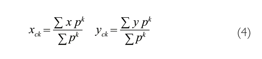
2.2 Circle Fitting Algorithm
For the circle fitting method,the center and radius of the laser spot are calculated by the edge points extracted in the edge detection step.The circle is fitted into a group of edge points,which are obtained by setting an appropriate threshold for simple differential operation alongx
direction andy
direction of CCD image data respectively
r
is the radius of the laser spot in CCD image data.The values ofx
,y
andr
can be determined by applying the least square method to minimise the residual between edge points and circles.2.3 Gaussian Fitting Algorithm
Gaussian fitting method is considered to be a very accurate method.It uses the typical Gaussian distribution of the laser spot,almost all the intensity information,and does not even need a good circular symmetric Gaussian distribution of semiconductor laser.Then,the center of laser spot is calculated by minimising the least square problem between Gaussian curve and laser spot profile.The strength distributionI
is given by:
I
is the max intensity of whole CCD,σ
andσ
are the standard deviations alongx
direction andy
direction of CCD image data,respectively.3 EXPERIMENTAL SETUP
The experimental setup of the device is as follows:place the circuit board on the anti-static sponge ensuring it is stable,calibrate the original position information of the circuit board,and use the host computer software to calculate the offset.Then,the coordinate position information of the components is deviated from thex
andy
directions by 0.5 mm,that is,our purpose is to measure four points of the components.The host computer software controls the 2D workbench,laser and commercial CCD (DAHENG MER-500-14GM),and records the actual height information of each electrical component through the spot detection algorithm,and use 4 pieces of height information to check whether the soldered part of the element is warped.The host computer software exports the obtained component height data to the designer in STL file format to check whether there is any space installation interference with the heat dissipation structure.Figure 3 and Figure 4 are the two-dimensional surface (worktable) drive board,communication board (open source) and the two-dimensional worktable equipped with laser and CCD.
Figure 3 2D stage driver board communication board(Open-source)

Figure 4 Hardware system (including LD and CCD)
As shown in Figure 5,four components are installed on the top of the PCB.They are power Metal-Oxide-Semi-conductor Field-Effect Transistor (MOS FET),which require an additional protruding structure to dissipate heat.As shown in Figure 6,at the bottom of the PCB,the space in the structure is limited.The top and bottom layout of PCB are shown in Figure 5 and Figure 6 respectively.

Figure 5 Original PCB top view

Figure 6 Original PCB bottom view
The test steps of the measuring device used in this paper are as follows:
1) Read the coordinate information file of high-power components selected;
2) Analyse the code,location,level and quantity of high-power components;
3) Perform the shortest path planning according to the location of high-power components;
4) Zero the 2D displacement table according to the edge or reference point of the circuit board;
5) Scan and measure the height of high-power components one by one according to step 3;
6) For a double-sided board,flip the board and repeat steps 4 to 5;
7) Read the DSN file containing high-power components;
8) Analyse thex
andy
dimensions of the outer contour of each high-power component;9) Generatex
andy
dimensions and measurement height information of the outer contour of each high-power component in Excel file,as well as STL model file of circuit board and components.4 EXPERIMENTAL RESULTS
In this section,the test results of typical optical class detection algorithms will be compared.Under the actual imaging conditions in the electronic assembly line,as shown in Figure 7,the laser spot reflected on the device surface is not only affected by speckle noise,as shown in Figure 7 (c),but also affected by the stamping of component marking giving irregular points and lines.Some studies show that similar occlusion before detecting the object has a great impact on the measurement results of laser spot,especially the relative measurement sensitivity.As described above,the results of the traditional algorithm introduced in this paper show the differences in imaging conditions,as shown in Figure 8.

Figure 7 Actual imaging conditions

Figure 8 Results of different laser spot center algorithms
Comparing the actual measured data,the error statistics and measure time are shown in Table 1.

Table 1 Statistical data of different laser spot center algorithms
Δρ
=[(Δx
)+(Δy
)]is the global position error,whereas Δx
,Δy
are the horizontal and vertical position errors,respectively.The irregular size of circuit board (46 mm×53 mm) was tested,and the height data of the tested components were obtained.There are 13 components on the circuit board.The STL 3D model exported by the host computer software is shown in Figures 9-11.

Figure 9 Heights of PCB top side components
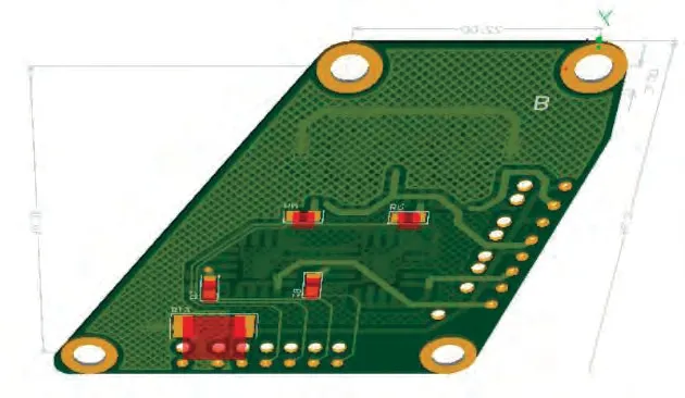
Figure 10 Heights of PCB bottom side components

Figure 11 PCB sectional view in STL file format
Through experimental results and preliminary analysis,we believe that the error mainly comes from the following aspects:
The algorithm error of laser spot center could be reduced by adjusting the CCD exposure so that the maximum intensity of the laser spot is close to saturation and not overflowing the CCD charge well.The measurement error of the laser stage can be reduced by using a multi-point average or median measurement.The user can choose the number of average points and the average method.The structure of the 2D stage can be strengthened and optimised in the future.The error caused by the accuracy of the 2D stage stepping motor,the minimum step control could be adjusted through the software according to the size of the component to 0.05 mm.Using the high-precision stepper-motor subdivision operation,the scanning speed will decrease.The host computer software can read the DSN file to obtain the component size,and then perform different subdivision motor control scans for different size components.As for the error caused by the step loss of the 2D stage stepper motor,at the current scanning speed,periodic calibrating of the reference point of the 2D stage can be considered.The PCB itself has some height error caused by warping and uneven placement.The surface area near the four corners and edge points of the PCB were measured to reduce the PCB height error.The experimental results show that Gaussian fitting is better than other methods under actual conditions.The opensource 2D stage could be optimised and restructured,and the test accuracy could be further improved.
By adjusting the CCD exposure,the algorithm error of the spot center can be reduced,the maximum intensity of the spot is close to saturation,so the CCD charge will not overflow.The error of measuring height displacement by laser goniometry can be reduced by multi-point average or median measurement.The structure of 2D displacement device can be strengthened and optimised in the future.Due to the error caused by the accuracy of 2D stepping motor,the minimum stepping control can be adjusted to 0.05 mm according to the size of components through software.Under the subdivision operation of high-precision stepping motor,the scanning speed will be reduced.The host software can read the DSN file to obtain the component size,and then perform different subdivision motor control scans for components of different sizes.For the error caused by a 2D step motor,the reference point of 2D displacement table can be periodically calibrated under the current scanning speed.PCB itself has some height errors,which are caused by warpage and uneven placement.Measurement of the area near the four blank area and edge points of PCB can reduce the PCB height error.The experimental results show that the accuracy of Gaussian fitting is better than other methods in practice,while the gray centroid algorithm has the fastest processing speed.
5 CONCLUSION
We have solved the task to find a low-cost and high-reliability method in measuring the height of components on a PCB.The PCB component height measurement device is built by using a commercial CCD and laser,open-source hardware and software.The experimental results show that the Gaussian fitting spot detection method is superior to other methods in accuracy,and the gray centroid algorithm is faster than other algorithms in processing.The error factors affecting the measurement were analysed.The proposed device has made it possible to measure the height of the components after PCB assembly,which can provide a reference for the iterative design during manufacture.
杂志排行

Aerospace China的其它文章
- Research on Key Issues for Mars Landing Missions
- LM-4B is Preparing for Launch
- Safety Design and Verification Analysis in the Satellite Development Stage
- Predict Aerodynamic Drag of Spacecraft in Very Low Earth Orbit Using Different Gas-Surface Interaction Models
- Study on the Multi-Component Test Technology of Solid Rocket Motors
- Gas Path Fault Tolerant Control of Aero-Engine Based on On-Board Model