Intercalation of germanium oxide beneath large-area and high-quality epitaxial graphene on Ir(111)substrate∗
2021-05-06XueyanWang王雪艳HuiGuo郭辉JianchenLu卢建臣HongliangLu路红亮XiaoLin林晓ChengminShen申承民LihongBao鲍丽宏ShixuanDu杜世萱andHongJunGao高鸿钧
Xueyan Wang(王雪艳), Hui Guo(郭辉), Jianchen Lu(卢建臣),Hongliang Lu(路红亮),2,‡, Xiao Lin(林晓),2, Chengmin Shen(申承民),2,Lihong Bao(鲍丽宏),2,3, Shixuan Du(杜世萱),2,3, and Hong-Jun Gao(高鸿钧),2,3
1Institute of Physics and University of Chinese Academy of Sciences,Chinese Academy of Sciences,Beijing 100190,China
2CAS Center for Excellence in Topological Quantum Computation,Chinese Academy of Sciences,Beijing 100190,China
3Songshan Lake Materials Laboratory,Dongguan 523808,China
Keywords: graphene,intercalation,heterostructure,tunneling barrier
1. Introduction
The extraordinary electronic, mechanical, and optical properties of graphene (Gr)[1]make it possible to produce high-performance electronic and optoelectronic devices, e.g.,field-effect transistors (FETs),[2,3]barristors,[4]high-speed photodetectors,[5–7]and light emitting devices,[8]if graphene is integrated with other materials, such as transition metal dichalcogenides (TMDs), semiconductors, oxides, etc. For scalable applications, large-scale and high-quality graphene is highly desired. Epitaxial growth on transition metal single crystal surfaces,[9–11]such as Ru(0001),[10,12]Ir(111),[13]Cu(111),[14]Pt(111),[11]Ni(111),[15]provides an effective way to fabricate large-area, high-quality, single-crystalline graphene. However, the strong interaction between graphene and metal substrates destroys the unique electronic structure and diminishes the intrinsic excellent properties of graphene.The conductive metal substrates also hinder its applications in electronics.
A transfer-free approach to address these challenges is to intercalate foreign atoms or molecules at the graphene/substrate interface. It has been reported that a few atoms,[16–20]molecules,[21]and binary compounds[22–25]can be intercalated between graphene and metal substrates.The intercalation effectively decouples graphene from the metal substrates and restores its intrinsic properties. On the other hand,the intercalation technique brings new opportunities to create graphene-based heterostructures. For example,graphene/silicene van der Waals heterostructures have been successfully fabricated by intercalation technique and exhibit a well-defined Schottky rectification behavior.[26]Of particular interest,the intercalation-fabricated graphene/SiO2/metal heterostructure behaves as a gated plate capacitor,in which the ultrathin SiO2layer acting as a homogeneous dielectric spacer provides possibility to tune the graphene overlayer[27]and enables the fabrication of graphene-based electronic devices.[28]Other graphene/oxide architectures have also attracted increasingly research interests due to the potential applications in devices such as tunnel junctions[29]and spintronics.[30]Recently,two-dimensional(2D)germanium was successfully intercalated at the interface of graphene and Ir(111).[31]Therefore,whether it is possible to form germanium oxide between graphene and metal substrate by intercalation has become an interesting topic, not only because Ge is a close neighbor of Si in the periodic table, but also because germanium oxide is expected to have a wider band gap[32]than germanium.
Here,we successfully intercalate germanium oxide at the interface of graphene and Ir(111). We first intercalate germanium beneath large-area high-quality epitaxial graphene on Ir(111). The interfacial germanium atoms are then further oxidized by oxygen intercalation. The underlying germanium oxide layer effectively decouples graphene from the Ir substrate,leaving graphene p-type doped. Low-energy electron diffraction(LEED),scanning tunneling microscopy(STM),and Raman characterizations confirm that the graphene layer is preserved after intercalation.The vertical transport measurements on such unique Gr/GeOx/Ir heterostructure reveal that the intercalated GeOxcan act as a tunneling barrier.
2. Experimental details
2.1. Sample preparation and characterizations
Graphene growth and germanium intercalation were carried out in an ultra-high vacuum (UHV) molecular beam epitaxy (MBE) system with a base pressure of about 2×10⁻⁹mbar. Firstly,Ir(111)crystal surface was cleaned by repeated cycles of sputtering and annealing(1370 K).Large-area high-quality graphene was then fabricated via thermal decomposition of ethylene molecules absorbed on Ir(111)surface at 1270 K.Germanium atoms were subsequently deposited onto the graphene surface at room temperature by electron-beam evaporation, and then the sample was annealed at 750 K for intercalation. The intercalated germanium was then oxidized by further oxygen intercalation. The oxidization process was realized by exposing the sample to oxygen with a pressure of 2.5 mbar at 500 K in a furnace cell. STM images were taken at ∼4.8 K. An Omicron Spectra LEED with a 4-grid detector was employed to identify the surface structure macroscopically. X-ray photoelectron spectroscopy(XPS)data were collected via a ThermoFisher Scientific ESCALAB 250x spectrometer using monochromatic Al Kαx-ray source. Raman spectra and maps were obtained by a commercial confocal Raman microscope (WiTec), using an excitation wavelength of 532 nm and a power of 2 mW.
2.2. Device fabrication and measurements
All the Gr/GeOx/Ir vertical heterostructure devices were fabricated by a standard electron-beam lithography technique followed by e-beam evaporation of Cr/Au (5/60 nm) as the contact electrodes. All electrical measurements were carried out in a vacuum chamber with a pressure lower than 10−5mbar,using a Keithley 4200-SCS system.
3. Results and discussion
Figure 1(a)schematically illustrates the procedure of germanium intercalation and oxidation at the interface between graphene and Ir(111). Large-area and high-quality monolayer graphene is epitaxially grown on a clean Ir(111) crystal surface. The germanium atoms are deposited onto the graphene surface,and then annealed to enable the intercalation. A subsequent exposure to oxygen leads to oxidation of the intercalated germanium layer. Each step is examined by XPS and the collected Ge 3d and C 1s core level spectra are shown in Figs.1(b)and 1(c). Before intercalation,the spectrum shows no germanium signal. After intercalation, the Ge 3d peak emerges and exhibits two narrow components due to spin–orbit splitting.[33]The Ge 3d peak is located at around 29 eV and no obvious peak shift is observed for Ir 4f before and after Ge intercalation (see Fig.S1 in supplementary material(SM)),indicating that the interfacial germanium is in elemental state rather than Ir germanide.[34]After oxidation, the Ge 3d peak evolves into a broad peak centered at 31.82 eV corresponding to Ge3+,indicating the formation of germanium suboxides.[35–37]Detailed oxidation process is shown in Fig.S2 in SM. There is no obvious peak shift for Ir after oxidation(see Fig.S1 in SM),suggesting that the Ir substrate is not oxidized. The thickness d of the GeOxlayer is roughly evaluated to be about 1.5 nm by the formula I =I0exp(−d/λGeOx).[38]The I0and I are the intensities of the Ir 4f7/2core level before and after GeOxintercalation, which are measured from the spectra shown in Fig.S1 in SM.The photoelectron escape depth in GeOx,λGeOx,is taken to be about 3 nm.[39]The electronic structures of graphene in different architectures are analyzed by measuring the C 1s core level spectra. As shown in Fig.1(c),the C 1s spectrum consists of a single narrow peak at 284.12 eV for the G/Ir sample,which shifts to 284.06 eV and 283.78 eV for samples of Gr/Ge/Ir and Gr/GeOx/Ir, respectively. The shifting of the C 1s peak suggests a p-type doping from both the intercalated Ge and GeOxlayers.
To examine the quality of the graphene layer before and after intercalation, both LEED and STM were employed to characterize the samples of Gr/Ir and Gr/GeOx/Ir. Figure 2(a)is the LEED pattern of the Gr/Ir sample, showing the sharp graphene spots(indicated by the arrow)and surrounding satellite spots due to moir´e superstructures between graphene and Ir(111)surface. We find that the graphene layer is single crystalline since individual LEED patterns obtained at different locations across the entire sample remain unchanged. From the corresponding large-area (Fig.2(b)) and atomically resolved(Fig.2(c)) STM images, we can clearly see defect-free honeycomb lattices of graphene. Combining LEED pattern and STM images,we confirm that the large-area and high-quality graphene has been fabricated on Ir(111)substrate. After germanium intercalation,the diffraction spots of graphene are still clear but the satellite spots almost disappear,and a new set of diffraction spots with 2×2 periodicity appear as previously reported,[31]implying that the intercalated Ge atoms form a 2×2 superstrucure with respect to Ir(111)rather than stay on the surface of graphene. After the subsequent oxygen intercalation, the results from LEED pattern demonstrate that the 2×2 spots of germanium disappear while the graphene spots keep high intensity,as shown in Fig.2(d). The corresponding STM image(Fig.2(e))shows that the topography becomes uneven.These results indicate that the interfacial germanium has been oxidized to form amorphous structures. We note that the graphene lattice is still intact after the Ge and O intercalation,as shown in Fig.2(f).
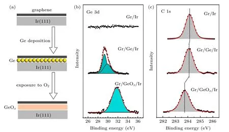
Fig.1. Schematic of the intercalation process and XPS spectra of samples at different stages. (a)Schematic showing the intercalation process of Ge and GeOx layer at the interface of epitaxial graphene and Ir(111)substrate. (b),(c)Ge 3d and C 1s core-level spectra of Gr/Ir,Gr/Ge/Ir,and Gr/GeOx/Ir,respectively.
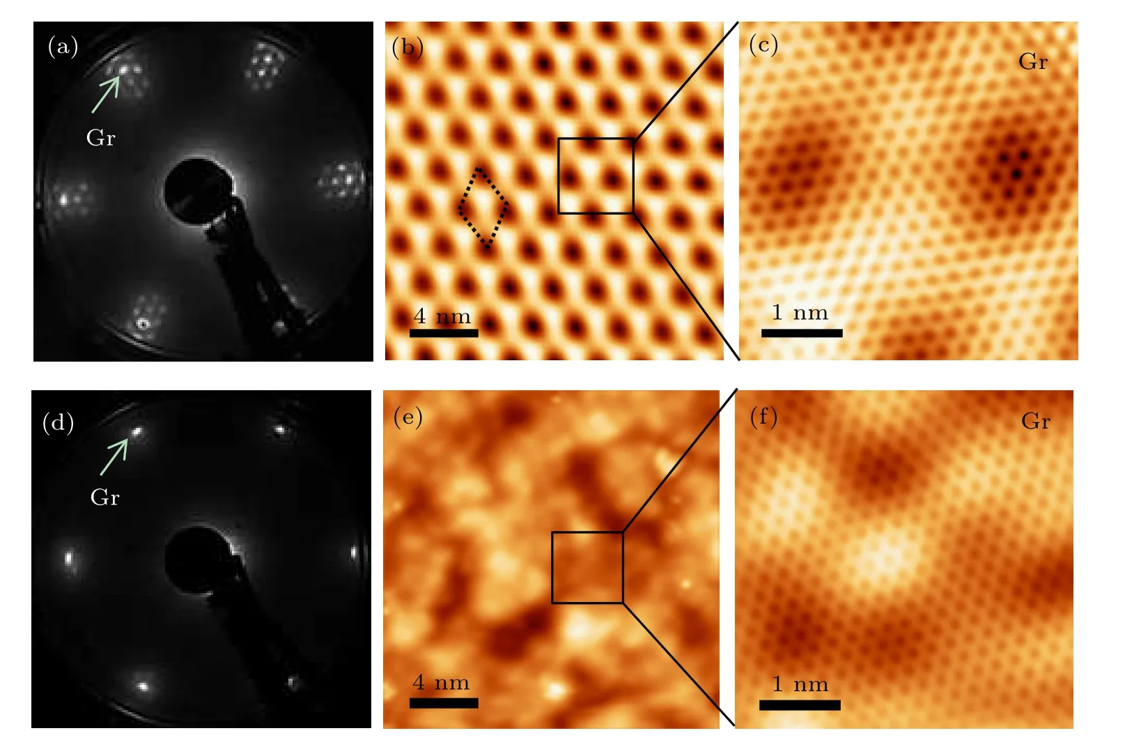
Fig.2. LEED patterns and STM images of Gr/Ir and Gr/GeOx/Ir. (a) LEED pattern, (b) the corresponding STM image (Vs =−1.54 V,It =0.05 nA), and (c) zoom-in STM image (Vs =0.05 V, It =0.3 nA) of Gr/Ir, showing a moir´e superlattice. (d) LEED pattern, (e) the corresponding STM image(Vs=−1 V,It=0.1 nA),and(f)zoom-in image(Vs=−1 V,It=0.6 nA)of Gr/GeOx/Ir,showing the formation of amorphous GeOx layer,and the top layer is graphene.
In order to probe the effect of GeOxintercalation on the topmost graphene and examine the properties of Gr/GeOx/Ir architectures, Raman measurements were performed on both as-prepared and intercalated graphene. In the left panel of Fig.3(a), the as-prepared epitaxial graphene on Ir shows no detectable Raman signals due to the strong hybridization between graphene π-band and the Ir substrate.[18,19,40]However,after the GeOxintercalation,the characteristic Raman features of graphene appear,suggesting that the intercalated GeOxlayers effectively decouple graphene from the Ir substrate. The weak D peak in the Raman curve suggests existence of very few defects in the intercalated graphene. The G band and 2D band shift to the higher energy by about 29 cm−1and 5 cm−1compared with those of pristine graphene, respectively, indicating charge transfer or strain induced by the underlying GeOxlayer.[41,42]Moreover, both G and 2D bands appear as narrow single peaks, and the 2D peak can be well fitted by a single Lorentzian peak with full-width at half-maximum(FWHM)∼42 cm−1(Fig.3(a)),suggesting that the graphene is single layer.[43]Raman maps of G peak position(left image of Fig.3(b))and corresponding histograms of G and 2D peak positions (see Fig.S3 in SM) show that the center positions of G band and 2D band remain almost constant, which indicates that the graphene has been decoupled over large area.The map of I2D/IGratio(right image of Fig.3(b))proves the single layer characteristic of graphene again. The contrast in the map of I2D/IGmay be caused by inhomogeneous strain in the graphene,[44]which can be introduced by uneven intercalated GeOxinterlayer. These results demonstrate that GeOxhas been intercalated under graphene uniformly and prove the formation of large-area Gr/GeOx/Ir architectures.
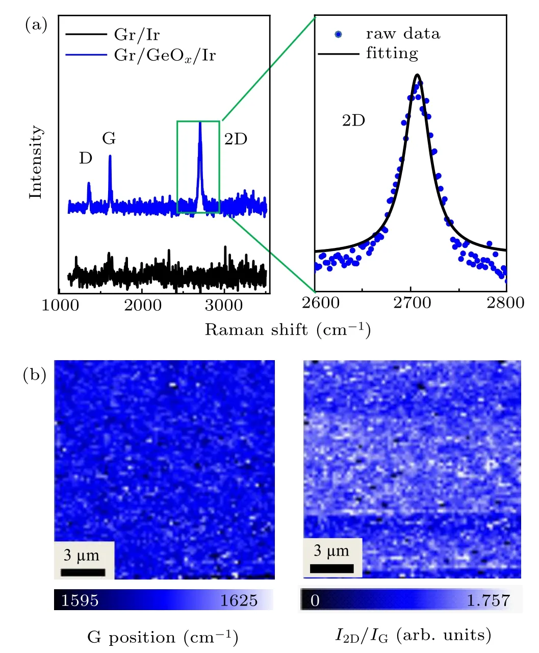
Fig.3. Raman characterizations of graphene. (a)Left: Raman spectra measured on Gr/Ir and Gr/GeOx/Ir. Right: 2D band of GeOx intercalated graphene and the fitting curve of single Lorentzian peak. (b)Raman maps showing the peak positions of G bands and the intensity ratio of 2D and G bands of Gr/GeOx/Ir,respectively.
To explore the potential applications of Gr/GeOx/metal vertical heterostructures, the current density–voltage (J–V)characteristics along the vertical direction were measured and shown in Fig.4(a). Such unique structures provide ultra-clean interfaces. The result shows obvious non-linear behavior,suggesting the existence of an energy barrier from the intercalated GeOx.The typical resistivity near zero-bias is ∼200 MΩ·µm2for the Gr/GeOx/Ir structure. The vertical current density in the Gr/GeOx/Ir structure at 10 mV bias and 100 K, as shown in Fig.4(b),is only ∼1×10⁻³A/cm2,indicating competitive insulating properties of the intercalated GeOxlayer. To obtain a better insight into the mechanism of transport through GeOxbarriers, the temperature dependence of the tunneling current is measured. For the Gr/GeOx/Ir heterostructure, the current across the intercalated GeOx(Fig.4(a)) shows a weak temperature dependence at low-temperature region and a strong temperature dependence at high-temperature region. It clearly shows a crossover(Tcross)at around 180 K,as demonstrated in Fig.4(b). The different transport behaviors at the two temperature regions suggest that there are two different dominating mechanisms. At temperatures higher than Tcross,the transport of carriers is dominated by thermal activation. While at temperatures lower than Tcross, the carrier transport is dominated by the tunneling process. The extracted barrier height is about 0.9 eV by Simmons fit based on the tunneling(see Fig.S4 in SM).[45,46]This vertical transport property is similar to that observed in Gr/WS2heterostructures, suggesting that the intercalated GeOxthin film can act as a tunneling barrier like WS2.
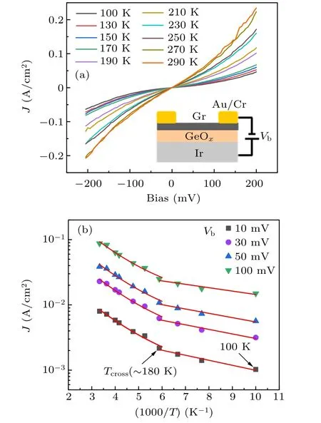
Fig.4. Transport measurements on vertical Gr/GeOx/Ir heterostructure. (a)Current density–voltage(J–V)characteristics of Gr/GeOx/Ir heterostructure at different temperatures. The inset is the schematic of the device structure. (b)Current density(J)as a function of the reciprocal of temperature at different bias voltage for Gr/GeOx/Ir heterostructure.
In our experiments, we found that the intercalated Ge is difficult to be oxidized in the MBE chamber. We realized the oxidation of intercalated Ge in a quartz tube furnace with a higher oxygen pressure and lower temperature. This two-step intercalation method, i.e., intercalation of one element in ultra-high vacuum MBE chamber and then oxidation in a furnace, may be helpful for intercalation of other oxides between graphene and metal substrates or construction of graphene/oxide heterostructures. In addition,the intercalation of germanium oxide interlayer can also serve as a universal method to study the intrinsic properties or promote the device performance of other low-dimensional structures.[47]
4. Conclusions
In summary,we have studied the germanium oxide intercalation of large-area and high-quality epitaxial graphene on Ir(111)by using LEED,STM,XPS,and Raman spectroscopy.First, germanium is intercalated below graphene, and then GeOxintercalation is realized through a subsequent intercalation of oxygen. Germanium oxide intercalation induces ptype doping of graphene. The graphene lattice keeps intact after intercalation, and more importantly, the intercalated layer effectively weakens the interaction between graphene and the substrate,making graphene more like the intrinsic one. Electrical transport measurements on Gr/GeOx/Ir heterostructure show two carrier-transport mechanisms at different temperature ranges, and the intercalated GeOxlayer can act as an effective tunneling barrier.
杂志排行

Chinese Physics B的其它文章
- Speeding up generation of photon Fock state in a superconducting circuit via counterdiabatic driving∗
- Micro-scale photon source in a hybrid cQED system∗
- Quantum plasmon enhanced nonlinear wave mixing in graphene nanoflakes∗
- Restricted Boltzmann machine: Recent advances and mean-field theory*
- Nodal superconducting gap in LiFeP revealed by NMR:Contrast with LiFeAs*
- Origin of itinerant ferromagnetism in two-dimensional Fe3GeTe2∗