Efficient Two-Dimensional Perovskite Solar Cells Realized by Incorporation of Ti3C2Tx MXene as Nano-Dopants
2021-03-15XinJinLinYangXiaoFengWang
Xin Jin, Lin Yang, Xiao-Feng Wang
ABSTRACT Two-dimensional (2D) perovskites solar cells (PSCs) have attracted considerable attention owing to their excellent stability against humidity; however, some imperfectness of 2D perovskites, such as poor crystallinity, disordered orientation, and inferior charge transport still limit the power conversion efficiency (PCE) of 2D PSCs. In this work, 2D Ti3C2Tx MXene nanosheets with high electrical conductivity and mobility were employed as a nanosized additive to prepare 2D Ruddlesden-Popper perovskite films. The PCE of solar cells was increased from 13.69 (without additive) to 15.71% after incorporating the Ti3C2Tx nanosheets with an optimized concentration. This improved performance is attributed to the enhanced crystallinity, orientation, and passivated trap states in the 3D phase that result in accelerated charge transfer process in vertical direction. More importantly, the unencapsulated cells exhibited excellent stability under ambient conditions with 55 ± 5% relative humidity.
KEYWORDS 2D perovskite solar cells; Ti3C2Tx nanosheets; Trap densities; Vertical orientation; Charge transport
1 Introduction
Over the last decade, various efforts have been aimed at converting solar energy to electricity through the photovoltaic effect with novel optoelectrical materials. In particular, organic-inorganic halide perovskites show great potential as excellent light-absorbing materials for photovoltaic devices [1-4]. Thus far, the power conversion efficiencies (PCEs) of organic-inorganic halide perovskite solar cells have been improved from 3.8 to 25.5% through optimization of low-cost solution processing [5, 6]. Although the outstanding photovoltaic performance of perovskite solar cells (PSCs) has attracted worldwide attention, PSCs usually exhibit severe instability to environmental factors, such as moisture, light, and heat, which greatly limits their further commercialization [7]. To address such stability issues, two-dimensional (2D) Ruddlesden-Popper (RP) perovskites with general chemical formula (A′)2An-1MnX3n+1, where n represents the number of layers of inorganic lead iodide slabs, A′, A, M, and X are a bulky long-chain organic spacer, a monovalent cation, a divalent metal cation, and a halide anion, respectively, have proven to be promising [8-11]. 2D RP perovskites are more thermally rigid, with larger cations impeding internal ion movement and allowing sufficient organic groups. That is, these compositions endow the absorber with hydrophobic properties resulting in improved stability in moist environment [12-14]. On the other hand, these structural components are offset by the large exciton binding energy and lower crystallinity [15, 16], which severely affect the separation and transport of carriers and ultimately lead to relatively low current and PCE values.
Current methods for orientation and crystal engineering of 2D RP perovskite films mainly include hot-casting [9], additive-assisted methods, and solvent engineering [17-29]. The hot-casting technique was used to prepare perovskite films, resulting in high-quality films with preferred growth orientation, which facilitates the transfer of charges along the vertical direction of the film; the disadvantage of this approach is that it is difficult to precisely control the temperature. A small amount of Cs+doping resulted in a significant efficiency improvement in 2D RP PSCs [22]. More recently, a PCE of 18.04% with a short-circuit current density (Jsc) of 17.91 mA cm-2was achieved in a (BA)2MA4Pb5I162D RP perovskite solar cell based on a water-assisted crystallization process; this translated into an increase in the Jsc(from 17.61 to 19.01 mA cm-2) and PCE (from 13.73 to 15.04%) values of the PSCs [30]. Low current values in 2D PSCs are mainly associated with poor charge transport [18, 31, 32]; therefore, carefully regulating the growth of 2D perovskite films to achieve a better vertical orientation is the key to overcome this problem [23, 33-35]. Despite great advances in the engineering of thin films, the efficiency of 2D RP PSCs is still behind that of their 3D counterparts, especially for the Jsc[36], and further work is needed to improve their efficiency to meet the commercialization requirement.
MXenes are 2D transition metal carbides and nitrides with a Mn+1XnTxcomposition, obtained by etching the A (Al, Sn, etc.) layer of the MAX phase, where M represents an early transition metal, X represents carbon and/or nitrogen, and Txindicates surface termination groups (usually -O, -OH, and/or -F) [37]. Ti3C2Tx, as the first discovered typical MXene, has many excellent properties, including high electrical conductivity, mobility, hydrophilicity, and flexibility [38], which are widely applied in energy storage, supercapacitors, sensors, catalysis, and electromagnetic interference shielding. In addition, Ti3C2Txhas been widely applied as a different component in solar cells. For instance, oxidized Ti3C2Txwas employed as electrode in dye-sensitized solar cells, resulting in a PCE of 2.66% [39]. Fu et al. [40] reported few-layered Ti3C2TxMXene-contacted Si solar cells with a record PCE of 11.5%. Yu et al. [41] applied Ti3C2Txmaterials both as electron- and hole-transport layers in organic solar cells and achieved a PCE of 9.06%. We demonstrated the use of UVozone-treated Ti3C2Txas electron transport layer (ETL) in PSCs and obtained a highly improved PCE of 17.17% [42]. Moreover, Ti3C2Txwas employed as an additive in SnO2[43] or TiO2/SnO2[44] multidimensional ETLs, obtaining a high PCE of more than 18%. Guo et al. [45] reported that Ti3C2Txdoping in the CH3NH3PbI3perovskite layer effi-ciently enhanced the crystal size and charge transfer of the film. Thus, Ti3C2TxMXenes have proven to be promising additives for PCE improvement, highlighting their great potential for application in the field of 2D PSCs, in which Ti3C2TxMXenes remain largely unexplored.
In this study, we for the first time fabricate PSCs employing the 2D (BA)2(MA)4Pb5I16RP perovskite absorber in which Ti3C2Txnanosheets were added as a nano-dopant. Systematic analyses showed that the addition of Ti3C2Txnanosheets in the precursor solution led to a homogeneous perovskite film formation during spin-coating process resulting in spontaneous passivation of grain boundaries. X-ray diffraction (XRD) measurements indicate that the incorporation of an optimal amount of Ti3C2Txnanosheets resulted in an enhanced crystallinity along with a preferential growth perpendicular to the substrate. Meantime, the multiphase coexistence in the 2D perovskite films could be modulated in a preferred order. These characteristics facilitated efficient charge transport, which boost the PCE from 13.69 to 15.71%, as the Jscincreases from 18.84 to 20.87 mA cm-2.
2 Experimental Section
2.1 Materials
Lead iodide (PbI2, > 99.99%), methylammonium iodide (MAI, > 99.5%), BAI (99.5%), and lithium-bis (trifluoromethanesulfonyl) imide (Li-TFSI, > 99%) were purchased from Xi’an Polymer Light Technology Corp. NH4SCN was purchased from Aladdin. 2,2′,7,7′-tetrakis-(N,N-dip-methoxyphenylamino)-9,9′-spirobifluorene (Spiro-OMeTAD, > 99.8%), 4-tert-butyl pyridine (tBP, 96%), and ultra-dry anhydrous N,N-dimethylformamide (DMF, 99.8%) and dimethyl sulfoxide (DMSO, 99.7%) were purchased from Sigma-Aldrich. All materials are not further purified before use.
2.2 Preparation of Ti3C2Tx MXene Hydrocolloid
The method is the same as our previous report. The 400-mesh uniform Ti3AlC2MAX powder was added into 12 M LiF/9 M HCl solution with continuously stirring for 24 h at room temperature. Specifically, 1.6 g LiF was added to 20 mL 9 M HCl solution at room temperature and stirred for 5 min. Then 1.0 g Ti3AlC2MAX powder was slowly added (about 5 min) to the etchant solution and continuously etched for 24 h at room temperature. After etching process, the obtained acid mixture was repeatedly washed over 6 times with deionized water by centrifugation at 8000 rpm for 5 min until the pH of mixture reached about 6. Finally, the slurry was sonicated for 30 min in an ice bath under argon and centrifuged at 3500 rpm for 1 h to separate the multi-layers. The obtained dark supernatant was the colloid solution of Ti3C2Txnanosheets, which could be used directly as the additive in 2D perovskite precursor. To confirm and tune the concentration of Ti3C2Txcolloid, a quantitative solution was filtered over a 0.22 µm pore sized cellulose membrane and the concentration of Ti3C2Txwas determined to be 11.6 mg mL-1by weighing the peeled-off dried film. Moreover, the solution was diluted to 5.8 mg mL-1by adding deionized water and sonicated for 30 min to control the average size to about 200 nm for better using as additive in perovskite precursor.
2.3 Preparation of 2D Perovskite Precursor Solution
The precursor solution of 2D perovskite BA2MA4Pb5I16(n = 5) was prepared by mixing BAI, MAI, PbI2, and NH4SCN in dimethylsulfoxide (DMSO) and dimethylformamide (DMF) solvents (5:5 volume ratio) with a stoichiometric ratio of 2:4:5:2; the concentration of Pb2+in the precursor solution was 1.2 M. Then, Ti3C2Txhydrocolloid (5.8 mg mL-1) was added to the perovskite precursor, at Ti3C2Txconcentrations of 0.1, 0.3, 0.5, and 0.7 mM. The solution was stirred for 8 h at 50 °C before use.
2.4 Film Preparation and Device Fabrication
The ITO-coated transparent substrates were cleaned with water, acetone, and alcohol in an ultrasonic bath for 30 min. After drying, the cleaned ITO substrates were treated with UV/ozone for 15 min before use. The SnO2colloid was diluted to 3 wt% by mixing with deionized water and spin-coated onto the ITO substrates at 3000 rpm for 30 s, followed by thermal annealing on a hot plate at 150 °C for 30 min and UV/ozone treatment for 15 min. Then, the UV/ozone-treated substrates were rapidly transferred into a glove box filled with argon, where the 2D perovskite films were fabricated by spin coating the precursor solutions onto the substrates at 4000 rpm for 30 s; during the spin coating process, 300 μL toluene was dripped onto the 2D perovskite film, followed by solvent annealing in DMF atmosphere at 100 °C for 10 min. To prepare the samples containing Ti3C2Tx, different amounts of Ti3C2Txwere introduced in the precursor solution. After the 2D perovskite film was cooled down to room temperature, spiro-MeOTAD was spin-coated on the 2D perovskite film at 4000 rpm for 30 s; the coating solution was prepared by dissolving 72.3 mg spiro-MeOTAD in 1 mL anhydrous chlorobenzene with 28.8 μL tBP and 17.5 μL Li-TFSI (520 mg mL-1acetonitrile) additives. The samples were kept overnight in the dark and dry air at room temperature. Finally, an 80-nm Ag electrode was thermally evaporated on top of spiro-MeOTAD under high vacuum (1 × 10⁻⁴Pa). The active device area was determined as 0.04 cm2by overlapping the Ag and ITO electrodes.
2.5 Characterization
2.5.1 Thin Film Characterization
UV/Vis absorption spectra were carried out with a Shimadzu UV-1900 spectrophotometer over wavelength range of 300-900 nm. The XRD patterns were recorded on Bruker D8 X-ray diffractometer with Cu Kα radiation (λ = 1.5418 Å) at room temperature (25 °C). The data were collected with a 0.02° step size (2θ) for 0.2 s. Top-view and cross-sectional scanning electron microscopy (SEM) images were acquired by a field emission scanning electron microscope (Hitachi SU8000) with an energy dispersive spectroscopy (EDS) system. The TEM images were recorded using a JEM-2200FS (JEOL). The roughness of perovskite films was characterized by using AFM (5500, Agilent, Santa Clara, CA). Steady photoluminescence (PL) measurements were carried out by RF-6000 spectrophotometer, while TRPL results were acquired by PL spectrometer (Edinburgh Instruments, FLS 920).
3 Results and Discussion
3.1 Characterization of Ti3C2Tx Nanosheets
Ti3C2Txnanosheets were obtained by etching the original Ti3AlC2powder, as described in the experimental section. To confirm the successful transformation of the raw Ti3AlC2powder into Ti3C2Txnanosheets, samples of Ti3AlC2powder and Ti3C2Txnanosheets were tested by XRD (Fig.1a). As can be seen in the figure, the disappearance of the strongest diffraction peak of Ti3AlC2(104) is accompanied by a shift of the (002) peak from 9.5° to about 7°, which indicates that the Al layer was successfully etched. The diffraction pattern of the Ti3C2Txnanosheets displays four sharp peaks at approximately 7°, 14°, 22°, and 28°, corresponding to the (002), (004), (006), and (008) facets, respectively, which is consistent with previous reports [43]. For the purpose of mixing the Ti3C2Txnanosheets with the perovskite precursor, smaller sized monolayered Ti3C2Txnanosheets were obtained by another 30 min of sonication, as shown in the SEM and transmission electron microscopy (TEM) images in Fig.1b, c, respectively. The size distribution results for the monolayer Ti3C2Txnanosheets show an average size of approximately 200 nm (Fig.1d). In order to apply Ti3C2Txnanosheets in perovskite devices, we incorporated Ti3C2Txhydrocolloid into the precursor solution, at concentrations of 0, 0.1, 0.3, 0.5, and 0.7 mM; in the following, the corresponding samples are labeled as control, Ti3C2Tx-0.1 mM, Ti3C2Tx-0.3 mM, Ti3C2Tx-0.5 mM, and Ti3C2Tx-0.7 mM, respectively.
2.5.2 Device Characterization
The J-V characteristics of perovskite solar cells were carried out by a Keithley 2400 source meter measurement system with an AM 1.5G filter at an illumination intensity of 100 mW cm-2, while the solar simulator was calibrated with a Si solar cell and the effective area of the cells was confirmed to be 0.04 cm2. The EQE spectra were measured using SOFN 7-SCSpecIII equipped with a 100 W Xe arc lamp, a filter wheel, and a monochromator. The EIS measurements of the devices were carried out on a Princeton electrochemical workstation (Parstat Mc Princeton Instruments Co., Ltd., USA); Z-View Analyst software was used to model the Nyquist plots obtained from the impedance measurements.
3.2 Photovoltaic Devices Performance
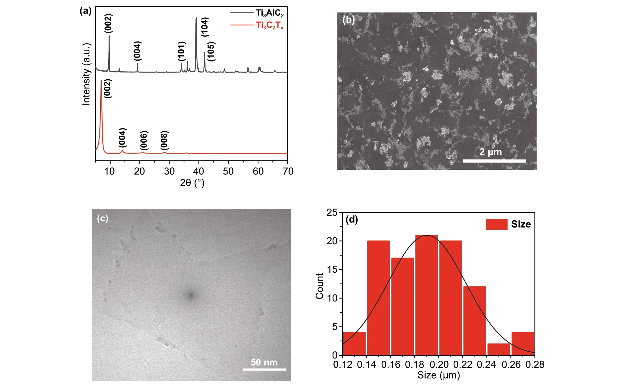
Fig.1 a XRD patterns of raw Ti3AlC2 powder and Ti3C2Tx nanosheets. b SEM and c TEM images of monolayer Ti3C2Tx nanosheets after sonication. d Particle size statistics for monolayer Ti3C2Tx nanosheets after sonication
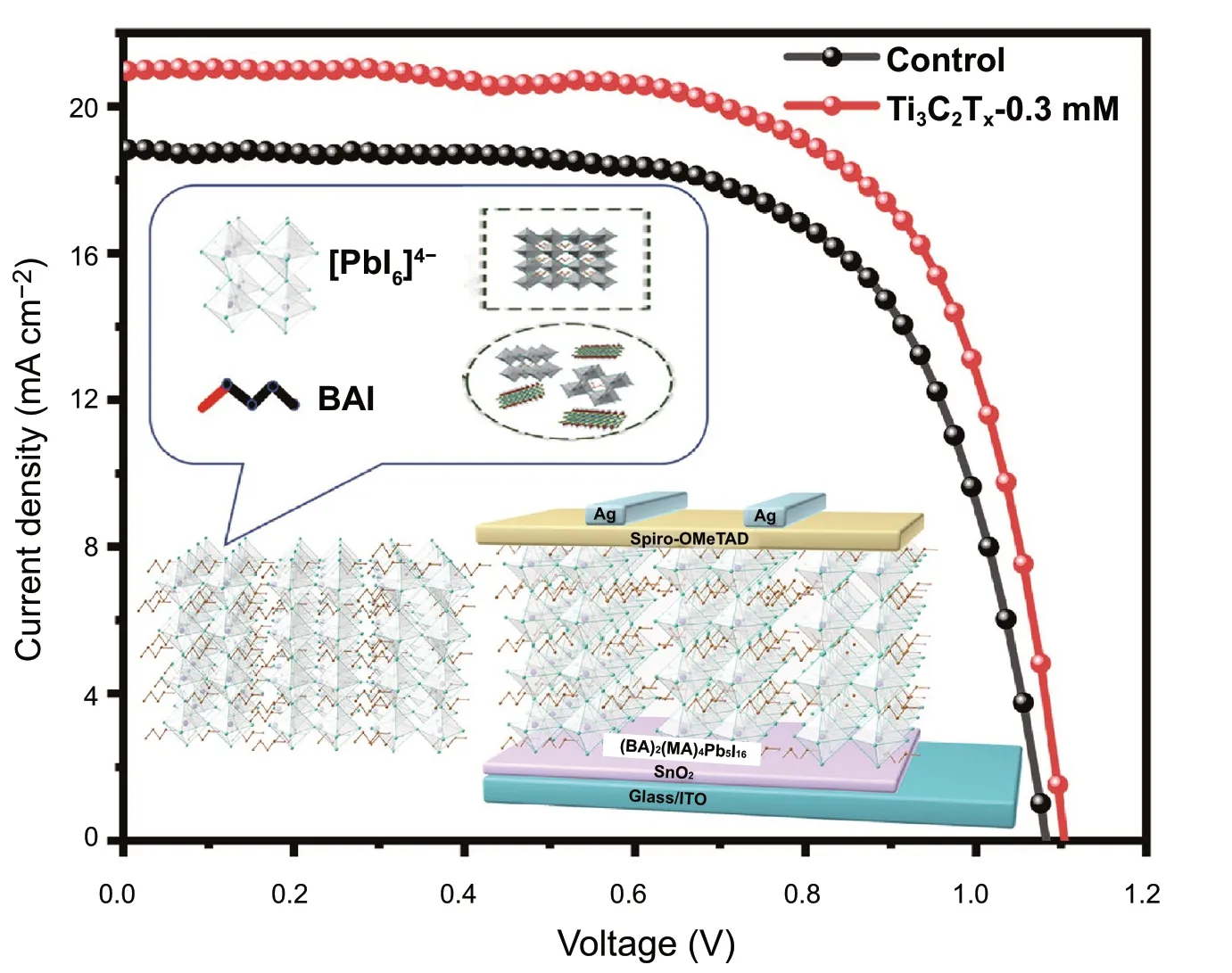
Figure 2a shows an architecture of the present PSCs together with the illustration of introducing Ti3C2Txinto the 2D perovskite film. To determine how different Ti3C2Txnanosheet contents affect the photovoltaic performance of 2D (BA)2(MA)4Pb5I16perovskite devices, we fabricated devices with an n-i-p planar architecture on the optically transparent electrode consisting of the indium tin oxide (ITO), the SnO2electron transporting layer (ETL), the 2D perovskite layer, the Spiro-OMeTAD hole transporting layer (HTL), and the Ag back electrodes. The J-V curves of devices fabricated with the control, Ti3C2Tx-0.1 mM, Ti3C2Tx-0.3 mM, Ti3C2Tx-0.5 mM, and Ti3C2Tx-0.7 mM samples are shown in Fig.2b. Table 1 summarizes the corresponding photovoltaic parameters. Overall, the PCE of the present devices increased and then decreased with increase in the Ti3C2Txcontent. The increase in the PCE of the devices is mainly attributed to the enhanced current density. In particular, the 2D perovskite device with optimal content of Ti3C2Tx-0.3 mM showed markedly increased Jsc(20.87 mA cm-2), open-circuit voltage (Voc) (1.11 V), and fill factor (FF) (67.84%) values, resulting in a greatly improved PCE of 15.71%, compared to a Jscof 18.84 mA cm-2, Vocof 1.09 V, FF of 66.7%, and PCE of 13.69% obtained for the control device. Clearly, the addition of Ti3C2Txnanosheets led to a significant improvement in photovoltaic performance. This improvement in the Jscis supported by the external quantum efficiency (EQE) spectrum shown in Fig.2c. The optimal devices prepared with the Ti3C2Tx-0.3 mM sample displayed a remarkable change, which can be explained by the marked light absorption associated with Ti3C2Txdoping. Based on the EQE spectra, the devices prepared with the control and Ti3C2Tx-0.3 mM samples had integrated current densities of 19.82 and 17.83 mA cm-2, respectively, within an error of 5%. More devices were fabricated to confirm the efficiency repeatability of devices incorporating the Ti3C2Txnanosheets. Figure S1 presents statistics of the relevant photovoltaic parameters obtained from more than 20 devices based on different doping amounts of Ti3C2Txnanosheets, showing that the average PCE of Ti3C2Tx-0.3 mM was 15.32%, which is much higher than the outstanding reproducibility of the control devices (average PCE = 12.11%). In addition, the photocurrent measured for more than 300 s at a maximum power point (0.80 V) indicates a stable power output, consistent with the J-V curves (Fig.2d).
3.3 Morphology Characterization
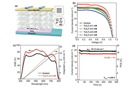
Fig.2 a Schematic diagram of devices with the structure of Glass/ITO/SnO2/2D perovskite/Spiro-OMeTAD/Ag. b J-V curves of devices with different amounts of Ti3C2Tx-doping. c EQE spectra and integrated Jsc of the control and optimized Ti3C2Tx-doping devices. d Stabilized power output and current density at a constant bias of 0.80 V for the Ti3C2Tx-doping devices

Table 1 Photovoltaic parameters of 2D PSCs with/without Ti3C2Tx additive
To understand what happened upon additional Ti3C2Txin perovskite layer, atomic force microscopy (AFM) and SEM were used to inspect the uniformity of the film on the surface of the samples before (control) and after addition of Ti3C2Tx. In Fig.3a, b, the top-view SEM images of Ti3C2Tx-0.3 mM show a homogeneous and dense pattern with almost no holes relative to the control film, which displays a highly rough surface and clear cracks. Probably, the small Ti3C2Txnanosheets are spontaneously distributed at the grain boundaries and defects of the intrinsic perovskite film. Such morphological change upon the Ti3C2Txincorporation must lead to the defect passivation. At other dopant concentrations, observable morphological changes were also observed for Ti3C2Tx-0.1 mM, Ti3C2Tx-0.5 mM, and Ti3C2Tx-0.7 mM (Fig.S3a-c). Increasing the amount of Ti3C2Txin the perovskite layer resulted in a rougher film surface, as further confirmed by AFM (Figs. 3c, d and S3d-f). It is clear that the appropriate amount of Ti3C2Tx-0.3 mM could induce a smoother film formation. The root-mean-square (RMS) roughness values of the film surface followed the order Ti3C2Tx-0.7 mM > control > Ti3C2Tx-0.5 mM > Ti3C2Tx-0.1 mM > Ti3C2Tx-0.3 mM, which is consistent with the SEM results. In addition, due to the extremely low content of Ti3C2Txrelative to PbI2, we could not use energy-dispersive X-ray spectroscopy (EDS) to confirm the presence of Ti3C2Txalong the grain boundaries (below the detection limits of EDS). Therefore, we determined the Ti3C2Txlocation in the film by increasing its amount to 2 mM. The elemental mappings of Pb, I, and Ti are shown in Fig.S4. The figure shows that the Ti species originating from the perovskite precursor were evenly distributed. Based on these observations, it can be concluded that the addition of trace amounts of Ti3C2Txsignificantly affected the surface morphology of the film. Therefore, the accurate control of the Ti3C2Txcontent is crucial to improve the photovoltaic performance of the devices.
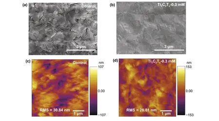
Fig.3 a, b Top-view SEM and c, d AFM image of the control and optimized Ti3C2Tx-doping perovskite films
3.4 Crystalline and Optical Property Analysis
In general, the excellent photovoltaic performance of 2D perovskite devices is strongly dependent on the crystallization and orientation of the film. Figure 4a displays the XRD patterns of the control and Ti3C2Tx-0.3 mM perovskite films. The stronger diffraction peaks of Ti3C2Tx-0.3 mM indicate a higher crystallinity in comparison with the control film. Both films show two primary diffraction peaks at approximately 14° and 28°, corresponding to the (111) and (202) crystal planes. As previously reported in literature [9], the (202) diffraction peaks indicate 2D perovskite films grown perpendicular to the substrate with vertical orientation, while the (111) crystal planes denote an inclined orientation. In the case of control and Ti3C2Tx-0.3 mM perovskite films, the weaker peak of the (111) crystal plane is accompanied by an enhanced (202) peak, as reflected by (202)/(111) ratios of 0.83 and 1.12, respectively, indicating a better vertical orientation for the Ti3C2Tx-0.3 mM perovskite film. As demonstrated by Shi et al. [18] using grazing-incidence wideangle X-ray scattering (GIWAXS), this property promotes the rapid transport of carriers in 2D perovskite films, leading to an increased current. Furthermore, it is worth noting that the overall XRD peaks of the Ti3C2Tx-based film slightly shifted toward lower diffraction angles, which can be attributed to the expansion of the cells by Ti3C2Txdoping. 2D perovskite films have a multiphase nature, and the presence of the characteristic peaks of (111) and (202) planes is likely a consequence of multiphase coexistence [46]. Therefore, the above peak shifts may also be related to the distribution of phases, as discussed below.
2D perovskite films often possess multiple phases due to quantum-well structures [47], as shown by the absorption spectra in Fig.4b. Multiple absorption peaks appear in the spectra of both control and Ti3C2Tx-0.3 mM films, such as those at 567, 598, 634, and 775 nm, corresponding to the perovskite phases with n = 2, 3, 4, and ∞, respectively. By comparing the intensity of the absorption curves, it can be seen that the Ti3C2Tx-0.3 mM perovskite films exhibited a stronger absorption at all wavelengths, due to enhanced light scattering and reflection [48]. The direct optical bandgaps of the control and Ti3C2Tx-0.3 mM perovskite films (Fig.S6) remained almost unchanged.
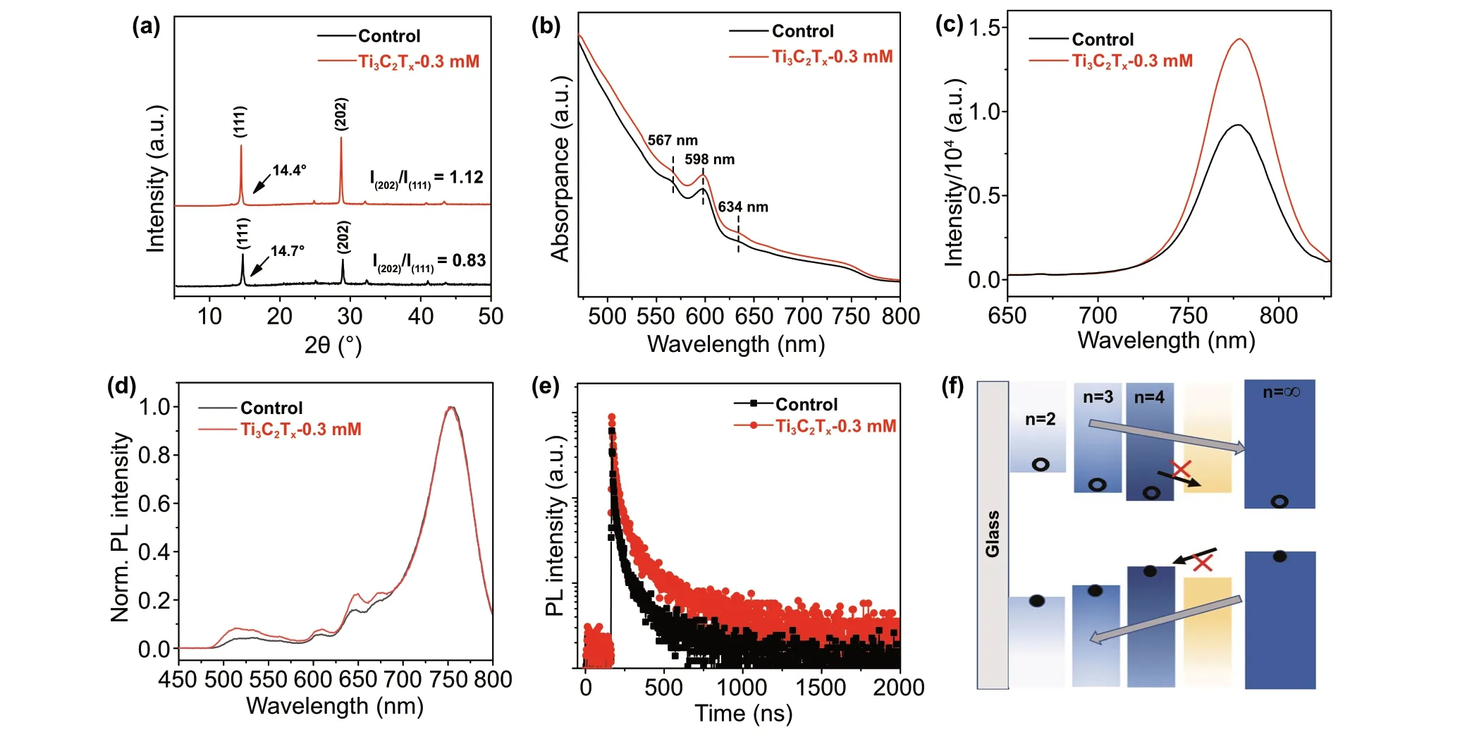
Fig.4 a XRD patterns, b UV/Vis absorption spectra, c, d PL spectra excited from front and back side and e time-resolved PL spectrums for the control and optimized Ti3C2Tx-doping perovskite films (on ITO substrates). f Illustration of band structure of 2D perovskite film
To further illustrate the multiphase distribution in the 2D perovskite film and the effects of Ti3C2Tx-0.3 mM doping, PL spectra under front (film) and back (ITO) side excitations are shown in Fig.4c, d. Upon front excitation, only one individual peak appeared in the spectra of both control and Ti3C2Tx-0.3 mM films, owing to the region of PL light excitation being confined close to the surface of the perovskite layer. According to previous reports [49], separate peaks originate from large-n phases on the surface of 2D perovskite films. Moreover, the stronger emission intensity of the Ti3C2Tx-0.3 mM films compared with that of the control reflects the suppression of non-radiative recombination, which can be related to the passivation of defects, in accordance with the SEM findings. Upon back excitation, we could observe phases with different small-n values, which is consistent with previous reports [46]. Surprisingly, Ti3C2Tx-0.3 mM led to a slight peak enhancement in the small-n phase of the bottom film, which can be explained by the kinetics of film growth after Ti3C2Tx-doping [18]. Due to the low solubility in the perovskite precursor, Ti3C2Txmay largely precipitate at the bottom of the film during spin coating and annealing, acting as a nucleation center for the lower-n phases within the bulk, which would increase nucleation of the small-n phases and ultimately favor a uniform phase distribution [50]. The enhancement in Jscis largely due to this feature. Liu et al. [51] proposed that the n = ∞ phase is predominantly distributed at the top of the film, with n = 2, 3, 4, and ∞ phases coexisting in the middle, and only small-n phases present at the bottom of 2D perovskite films. However, the small-n phases existing in the intermediate mixing region can act as shallow traps in 2D bulk perovskites [51, 52], blocking charge separation and transport, and ultimately greatly affecting the Jscof the devices. Ti3C2Txdoping can suppress the density of these shallow traps and thus extend the lifetime of the carriers, as shown in Fig.4e. The time-resolved PL spectrums show that the Ti3C2Tx-0.3 mM film exhibited longer average lifetimes compared to the control film. The fit formula and relevant parameters of carrier lifetimes are summarized in Table S2. This finding is a good indication that the addition of Ti3C2Txcan inhibit non-radiative recombination losses and thus enhance Jsc. The sequential spatial distribution in the order of n values is illustrated in Fig.4f. With an ordered distribution of n values, photogenerated excitons are effi-ciently dissociated into electrons and holes, shifted in opposite directions, and eventually collected by the electrode.
3.5 Carrier Dynamics
Current density versus incident light intensity plots were used to illustrate the dynamics of carrier recombination in devices, which follows the relationshipJsc∝Iα, as shown in Fig.5a. The Ti3C2Tx-0.3 mM device shows a relationship more closely related to the ideal factor ( α=1 ) on a doublelogarithmic scale, with a value of 0.961, compared to a value of 0.953 for the control device; this indicates a lower degree of bimolecular recombination [25], which may be largely attributed to the reduction in trap density, consistent with the SEM observations. In order to quantify the passivation effect of the device upon addition of Ti3C2Txnanosheets, we measured dark I-V curves of devices with SnO2/2D perovskite/PCBM/Ag structure, as shown in Fig.5c, d. The relevant details of the calculation can be seen in the supporting information. The calculated defect density of the Ti3C2Tx-incorporating devices was 0.89 × 1015cm-3, which is lower than that of the control device (1.16 × 1015cm-3), suggesting an improved quality of 2D perovskite film after Ti3C2Tx-doping.
Subsequently, we examined the characteristics of both devices through electrochemical impedance spectroscopy (EIS) measurements and the Nyquist plots shown in Fig.5b, with the equivalent circuit model displayed in the inset. Here, Rsrepresents the series resistance, which primarily reflects the electrical contacts, wires, and sheet resistance of the electrodes [53]. The charge-transfer properties at the interface are reflected by the charge-transfer resistance (Rtr), whereas Rrecis related to the recombination of the carriers [54]. It is clear that the Rsvalues of the two devices were similar. However, there was a significant variation in the Rtrvalue upon Ti3C2Txdoping. Obviously, the Ti3C2Tx-0.3 mM sample displayed a lower Rtrvalue, indicating an optimal charge transfer, which can be explained in terms of the charge-transfer speed at the perovskite/ETL and perovskite/HTL interfaces. The apparent negative relationship between the Rtrvalue and Ti3C2Txdoping implies that the charge transport at the surface greatly affects the Jscand PCE values.
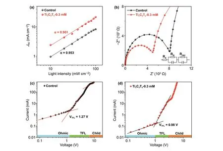
Fig.5 a Jsc versus light intensity and b Nyquist plots of EIS with the equivalent circuit for the control and optimized Ti3C2Tx-doping perovskite devices. c, d I-V curves of the electron-only devices under dark based on the control and optimized Ti3C2Tx-doping
3.6 Devices Stability
In contrast to 3D perovskites, excellent stability has always been a characteristic feature of 2D perovskites [12, 55]. The unencapsulated perovskite devices were placed in an environment with 55 ± 5% humidity to monitor their longterm stability. After a certain period of time, the devices were re-exposed to standard light intensity to test their PCE values, as shown in Fig.6. Overall, the 2D perovskite devices exhibited superior long-term stability in comparison with their 3D counterparts, with almost no degradation after 300 h. Satisfactorily, the Ti3C2Tx-based devices maintained 80% of their original PCE value after up to 750 h, while the PCE of the control devices was reduced to 40% of the initial value after 700 h of storage. In addition, we examined the thermal stability of 2D perovskite films with/without the presence of Ti3C2Tx. Figure S7 shows the dependence of absorption intensity reflecting the degradation of 2D perovskite films on continuous heating at 150 ℃ in a N2-filled glove box. Compared to Ti3C2Tx-0 mM perovskite film (original film), Ti3C2Tx-0.3 mM perovskite film remains almost unchanged after 12 h in the absorption intensity. After 48 h of thermal aging test, the absorption intensity of Ti3C2Tx-0 mM perovskite film is substantially decreased, whereas no serious decrease in the absorbance was observed in Ti3C2Tx-0.3 mM perovskite films. This result indicates that the presence of Ti3C2Tximproves the thermal stability of 2D perovskite films. It has been reported that when the perovskite devices are exposed to water molecules in the air or continuous high temperature, the additives in Spiro-OMeTAD will diffuse into the perovskite film and the organic components will escape from film to damage the film structure, and eventually leading to film decomposition [56]. The Ti3C2Tx-containing perovskite precursor solution is spin-coated onto the substrate, and Ti3C2Txin the bulk phase will induce the protonation with CH3NH3(MA), because the surface fluorine terminal groups of Ti3C2Txhave a strong interaction with hydrogen atoms of MA [45], which results in the superior crystallinity of the Ti3C2Tx-doped perovskite films (Fig.4a). In addition, a portion of the Ti3C2Txnot inserted into the perovskite lattice will stay at the crystal boundary to passivate defects, as shown in Fig.3b. Besides, the improved stability of the Ti3C2Tx-based samples compared to the control sample can also be attributed to the van der Waals interaction that significantly stabilize the framework of 2D perovskite films, resulting in highly oriented crystals with fewer detrimental defects. Moreover, previous studies suggest that species with low-n values in the perovskite layer will produce a passivated layer blocking further degradation [12, 57]. Therefore, the incorporation of Ti3C2Txin perovskite devices provides joint consequence of above effects leading to a higher long-term stability.
4 Conclusion
In summary, we have shown that a moderate doping level of Ti3C2Txnanosheets can greatly improve the quality of 2D perovskite (BA)2(MA)4Pb5I16films as well as the photovoltaic performance of the corresponding device, with an increase in PCE from 13.69 to 15.71%, owing to a significant increase in current. The superiority of the Ti3C2Tx-doped devices is mainly attributed to the intensified crystallinity, vertically oriented growth, and homogeneous phase distribution in the thin film, which ultimately facilitates charge transport. In addition, the Ti3C2Txnanosheets-doped devices exhibit a relatively higher humidity stability than the raw devices, owing to the better crystallinity and passivation effect of perovskite films. This work provides an effective strategy for improving the performance of 2D perovskite films and further expands the applications of Ti3C2Txin photovoltaics.
AcknowledgementsXin Jin and Lin Yang contribute equally to this work. This work was supported by the National Natural Science Foundation of China (No. 11974129 to X.-F. W.) and “the Fundamental Research Funds for the Central Universities, Jilin University.”
Open AccessThis article is licensed under a Creative Commons Attribution 4.0 International License, which permits use, sharing, adaptation, distribution and reproduction in any medium or format, as long as you give appropriate credit to the original author(s) and the source, provide a link to the Creative Commons licence, and indicate if changes were made. The images or other third party material in this article are included in the article’s Creative Commons licence, unless indicated otherwise in a credit line to the material. If material is not included in the article’s Creative Commons licence and your intended use is not permitted by statutory regulation or exceeds the permitted use, you will need to obtain permission directly from the copyright holder. To view a copy of this licence, visit http://creat iveco mmons.org/licen ses/by/4.0/.
Supplementary InformationThe online version contains supplementary material available at https://doi.org/10.1007/s4082 0-021-00602-w.
杂志排行
Nano-Micro Letters的其它文章
- Interior and Exterior Decoration of Transition Metal Oxide Through Cu0/Cu+ Co-Doping Strategy for High-Performance Supercapacitor
- Lead-Free Perovskite Materials for Solar Cells
- Berlin Green Framework-Based Gas Sensor for Room-Temperature and High-Selectivity Detection of Ammonia
- Highly Sensitive Ultrathin Flexible Thermoplastic Polyurethane/Carbon Black Fibrous Film Strain Sensor with Adjustable Scaffold Networks
- A Review on Metal-Organic Framework-Derived Porous Carbon-Based Novel Microwave Absorption Materials
- Ultrasonic Plasma Engineering Toward Facile Synthesis of Single-Atom M-N4/N-Doped Carbon (M = Fe, Co) as Superior Oxygen Electrocatalyst in Rechargeable Zinc-Air Batteries
