Epitaxial Lift-Off of Flexible GaN-Based HEMT Arrays with Performances Optimization by the Piezotronic Effect
2021-03-15XinChenJianqiDongChenguangHeLongfeiHeZhitaoChenShutiLiKangZhangXingfuWangZhongLinWang
Xin Chen, Jianqi Dong, Chenguang He, Longfei He, Zhitao Chen, Shuti Li, Kang Zhang , Xingfu Wang , Zhong Lin Wang
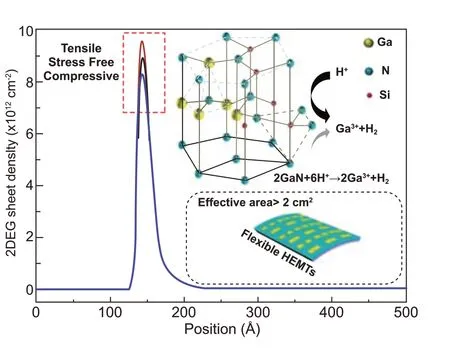
ABSTRACT High-electron-mobility transistors (HEMTs) are a promising device in the field of radio frequency and wireless communication. However, to unlock the full potential of HEMTs, the fabrication of large-size flexible HEMTs is required. Herein, a large-sized (> 2 cm2) of AlGaN/AlN/GaN heterostructure-based HEMTs were successfully stripped from sapphire substrate to a flexible polyethylene terephthalate substrate by an electrochemical lift-off technique. The piezotronic effect was then induced to optimize the electron transport performance by modulating/tuning the physical properties of two-dimensional electron gas (2DEG) and phonons. The saturation current of the flexible HEMT is enhanced by 3.15% under the 0.547% tensile condition, and the thermal degradation of the HEMT was also obviously suppressed under compressive straining. The corresponding electrical performance changes and energy diagrams systematically illustrate the intrinsic mechanism. This work not only provides in-depth understanding of the piezotronic effect in tuning 2DEG and phonon properties in GaN HEMTs, but also demonstrates a low-cost method to optimize its electronic and thermal properties.
KEYWORDS AlGaN/AlN/GaN heterojunction; Epitaxial lift-off; Flexible membrane; Two-dimensional electron gas; Piezotronic effect
1 Introduction
Owing to their high breakdown field strength, superior electron saturation drift speed, and excellent thermal conductance, nitride semiconductors have been widely used in various electronic/optoelectronic devices, such as light-emitting diodes (LEDs) [1, 2], photosensors [3-5], and high electron mobility transistors (HEMTs) [6, 7]. Among them, AlGaN/AlN/GaN heterostructure-based HEMTs take advantage of the high-density and high-mobility two-dimensional electron gas (2DEG) at the heterojunction interface, which has received much attention and shows extensive application prospects for radio-frequency (RF) devices and wireless transmission modules in communication. Future systems for HEMTs in intelligent devices, wireless communication and wearable devices have generated a demand for integration into diverse applications, circuits, platforms, and geometries. To more effectively accomplish this, the entire device will require a small footprint, possess flexural properties enable wireless systems to be placed onto nonplanar platforms or surfaces, and improve overall mechanical reliability. Significant efforts of flexible HEMTs have been made in strainable radio-frequency device [8], strain-controlled power devices (SPDs) [9], etc. However, the lattice tolerance and high growth temperature (> 1000 °C) [10] restrict their epitaxial growth mainly on rigid sapphire, SiC and/or Si by metal-organic chemical vapor deposition (MOCVD). In addition, the maximum potential of the HEMT is also limited by the high working temperature induced by nearjunction Joule heating and insufficient rate of heat removal from the active device regions to the substrate, which significantly reduces the output performance and reliability [11, 12]. Mitigation of the thermal-induced degradation of HEMTs is strongly necessary. Therefore, the focus of implementing bendable HEMTs is to exfoliate from the original growth substrate and transfer to flexible substrates with high thermal conductivity. In addition, flexible substrates provide different functions such as flexible structures, stretchable structures, and curved conformal installations, which induce complex stress distribution to greatly affect the electrical characteristics [13]. Some transfer techniques have been reported and are shown in Table 1, such as the laser lift-off technique [14, 15], chemical lift-off (CLO) [16], mechanical lapping and etching of silicon-based HEMTs [17], and introducing an atomic-thickness release layer [18, 19], which increases the cost and risk due to the involvement of bulky and expensive equipment and/or strong acid. In addition, conductivity-selective electrochemical (EC) etching by preparing pre-holes on the epitaxial wafer layer [20, 21], inevitably destroys the effective area and integrity of NMs and largely limits the subsequent applications. Thus, it is necessary to develop a cost-effective and high-efficiency method for fabricating large bendable HEMTs.
The piezotronic effect, a bridge connecting the piezoelectric property and non-centrosymmetrical semiconductors has been applied to optimize the performance of various nanodevices and demonstrate many novel applications [22, 23]. External-strain applied along the polar direction of noncentrosymmetrical semiconductors can generate piezoelectric polarization charges (piezo-charges) at the homo-/heterojunction interfaces. These piezo-charges could modify the energy band and/or the local barrier height and ultimately affect the carrier transport. As mentioned above, the AlGaN/AlN/GaN heterostructures have strong spontaneous polarization and piezoelectric polarization, which results in the generation of net static charges and 2DEG at the interface. Under external stress conditions, the external strain-induced piezopotential ( Ppiezo) would couple with the intrinsic spontaneouspolarization ( Psp) and lattice-mismatch-induced piezoelectric polarization ( Plm). The coupling between these polarizations would fundamentally modify the energy band and change the charge density at the local heterojunction, and thus affect the performance of the HEMTs.

Table 1 Previous reported transfer methods on GaN based nanomembranes (NWs)
In this work, an electrochemical lift-off (ECLO) technique was adopted to peel AlGaN/AlN/GaN HEMT arrays from a sapphire substrate. A large nitride membrane with HEMT arrays was successfully separated from the sapphire substrate and transferred onto a polyethylene terephthalate (PET) flexible substrate. The analysis of the crystal quality indicates that the transferred membrane exhibited a decreased dislocation density. Moreover, the flexible devices showed a high saturation current of 105.67 mA mm-1under zero gate voltage and excellent transconductance of 27.17 mS mm-1at Vds= 10 V. The piezotronic effect study indicated that the saturation current increased by 3.15% under the 0.547% tensile strain condition. In addition, the effects of external strain on the phonon properties and thermal conductivity of the flexible AlGaN/AlN/GaN HEMTs were systematically investigated. Under the compressive state, the saturation current attenuation of the device caused by thermal degradation was significantly mitigated. This study illustrates the intrinsic mechanisms of a 2DEG and thermal conductivity modulated by the piezotronic effect and endeavors to open up new ways to expand the practical applications of GaN-based HEMTs in flexible electronics.
2 Experimental Section
2.1 Synthesizing AlGaN/AlN/GaN Heterostructure Membrane
The multilayer epi-structure was fabricated by MOCVD. The trimethylgallium (TMGa), trimethylaluminum (TMAl), trimethylindium (TMIn), and ammonia (NH3) were used as Ga, Al, and N sources, respectively. N2and H2were used as carrier gases in the growth process. First grown on the sapphire substrate was a u-GaN (unintentional doped) layer, followed by a lightly doped n-type GaN (Si doping concentration of 5 × 1018cm-3, 500 nm in thickness) layer, to improve the tangential current flow. After depositing another u-GaN (900 nm) layer which protects the n-GaN was a sacrificial layer (n+-GaN, n = 1.0 × 1019cm-3, thickness of 1500 nm). The uppermost structure applied was an AlGaN/AlN/GaN heterojunction with a total thickness of 931.5 nm (Al0.3Ga0.7N layer of 30 nm, AlN layer of 1.5 nm; u-GaN of 900 nm). The detailed growth conditions are described in the following. GaN was synthesized at 1050 °C and 400 mbar in hydrogen for 1680 s using TMG (22 μmol min-1) and NH3(67 mmol min-1). Afterward, an ultrathin AlN interlayer was deposited at 1100 °C for 8 s using TMAl (5.3 μmol min-1) and NH3(90 mmol min-1). Finally Al0.3Ga0.7N layer was grown at 1200 °C for 50 s using TMGa (12.3 μmol min-1), TMGa (4.6 μmol min-1), and NH3(110 mmol min-1). Before the device was prepared, the epitaxial wafer was cleaned with acetone, isopropanol, and deionized water, in that order. Subsequently inductively coupled plasma (ICP) was used to perform dry etching to form isolation regions, and finally photolithography was performed to form electrode patterns. The corresponding electrodes were fabricated by electron beam evaporation. The source and drain electrodes required ohmic contact; thus, four layers of metal Ti/Al/Ni/Au (20/130/50/100 nm) were deposited and then rapidly annealed in a nitrogen atmosphere at 850 °C for 30 s. As gate electrode required Schottky contact, electron beam evaporation was further used to deposit Ni/Au (30/300 nm). The gate length was 2 μm, the gate width was 60 μm, and the source-gate and drain-gate spacing were 3 μm and 10 μm, respectively.
2.2 External Strain Calculations
External strains along the c-axis were applied to the AlGaN/AlN/GaN heterostructure membrane by locking the device between a one-dimensional displacement stage and a steady rest as shown in Fig.S6. By rotating the knob, a compressive or tensile strain was applied to the devices. For facilitate discussion, the bending strain was converted to the normal strain ε [24].
2.3 Materials Characterization
The detailed microscopic structures of the epi-structures and the AlGaN/AlN/GaN heterostructure membrane were characterized by optical microscopy (LEICA DM500), scanning electron microscopy (SEM, ZEISS Ultra 55), transmission electron microscopy (TEM, JEM-2100HR) with selected-area electron diffraction (SAED), high-resolution HRTEM (HRTEM, JEM-1400 PLUS), Raman spectrometry (invia), Raman spectrometry (invia), high-resolution X-ray diffractometry (HRXRD, RIGAKU Smartlab 9 kW), and a Source/Measure Unit (Keysight B2902A) combined with a probe station.
3 Results and Discussion
3.1 Device Structure and Basic Characteristics
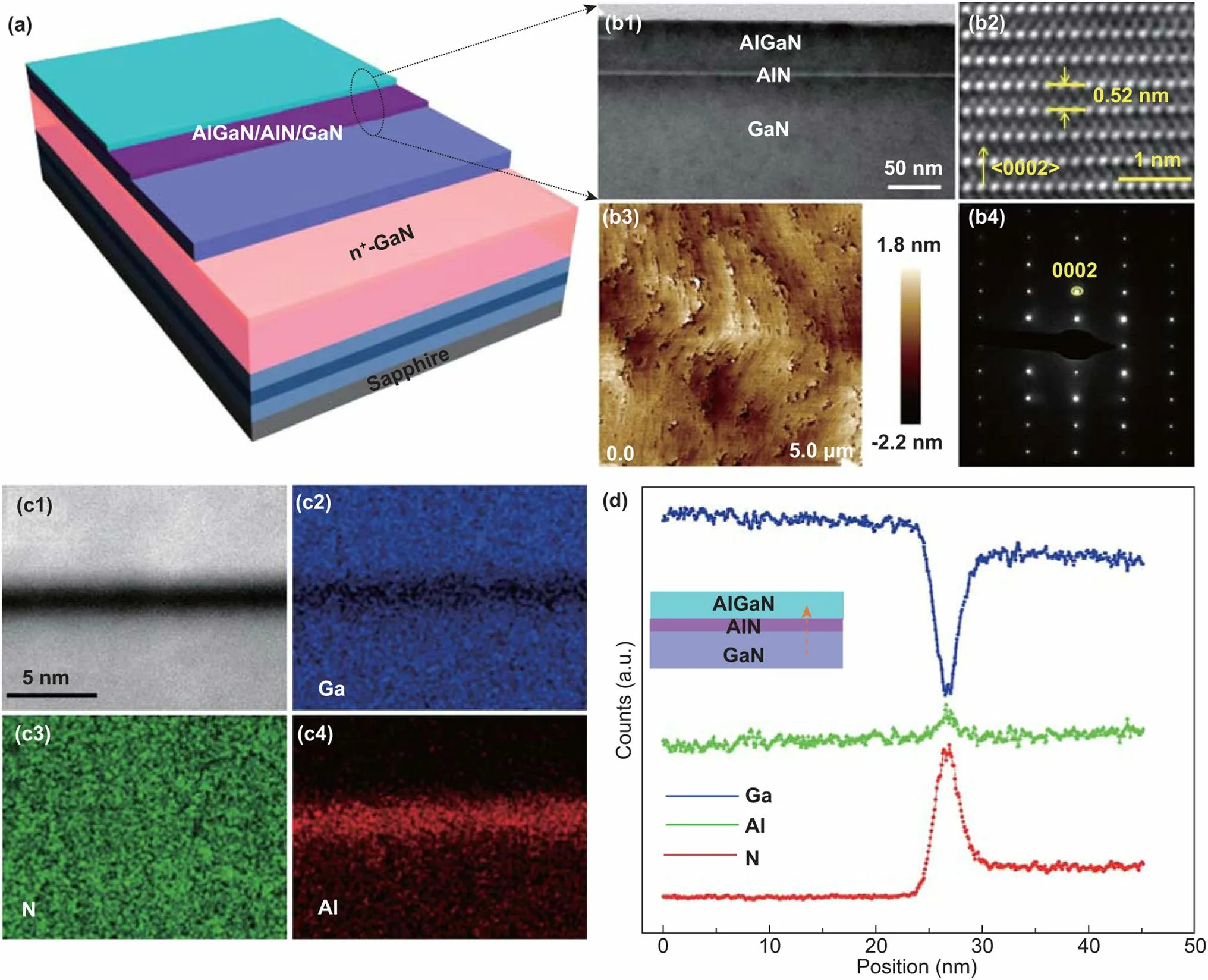
Fig.1 Structural characterization of AlGaN/AlN/GaN heterostructure membrane. a Schematic diagram of the heterostructure membrane on sapphire. b1 The scanning transmission electron microscopy (STEM) image of AlGaN/AlN/GaN interface, the scale bar is 50 nm. b2 The highresolution transmission electron microscope (HRTEM) image. b3 AFM image of heterostructure membrane on sapphire. b4 The selected area electron diffraction (SAED) pattern taken from the same area of HRTEM. c1 HAADF-STEM image collected from heterostructure membrane. c2-c4 STEM energy-dispersive X-ray spectroscopy (EDX) elemental image of the AlGaN/AlN/GaN heterostructure. d The EDX line profiles for Ga (blue line), Al (green line), and N (red line) elements
Using MOCVD, the epitaxial structure was fabricated as shown in Fig.1a. Details about the epitaxial multilayers were presented in Experimental Section. A specifically designed sacrificial layer (highly conductive GaN) was inserted between the AlGaN/AlN/GaN heterostructure and the GaN nuclear layer grown on sapphire, which was selectively etched in the ECLO process. Figure 1b1 shows a typical scanning transmission electron microscopy (STEM) image of an AlGaN/AlN/GaN interface, in which the white contrast line reveals the existence of an AlN ultrathin layer (1.5 nm). An HRTEM image of GaN is shown in Fig.1b2; the interplanar spacing in the (0002) direction is 0.52 nm, which is consistent with bulk GaN [25]. The surface of the heterostructure membrane exhibits an atomically flat surface morphology under atomic force microscopy (AFM) (Fig.1b3) with a root-mean-square roughness of less than 0.542 nm determined from an area of 5 × 5 μm2. In addition, the SAED pattern (Fig.1b4) demonstrates that the epitaxial growth direction is along the < 0002 > c-axis. These morphological characterizations indicate that the GaN barrier underneath the ultrathin AlN layer is in a relaxed state and AlGaN/AlN/GaN heterostructure has outstanding epitaxial quality. The high-angle annular dark-field STEM (HAADF-STEM) image clearly shows the sandwich structure in Fig.1c1 resulting from the insertion of AlN, and the corresponding spatial distributions of Ga, Al, and N elements are shown in Fig.1c2-c4, which are the STEM energy-dispersive X-ray spectroscopy (EDX) elemental mapping of AlGaN/AlN/GaN heterostructure membrane. Along the direction from GaN to AlGaN, the results of EDX line-scan mapping were extracted and plotted in Fig.1d. The sudden decrease/increase in the Ga/Al element further proves the existence of an ultrathin AlN layer and abrupt heterojunction interfaces.
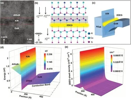
Fig.2 Atomic characterization of AlGaN/AlN/GaN heterostructure membrane. a The STEM image of heterostructure membrane. The scale bar is 3 nm. b Corresponding atomic structure along the c-axis. c The diagram of conduction band profile and 2DEG. d The calculated conduction band and valence band. e The calculated 2DEG sheet density in AlGaN/AlN/GaN heterostructure membrane

In order to acquire freestanding AlGaN/AlN/GaN HEMTs, ECLO was adopted. The advantages of ECLO are that it can be qualitatively selected based on differences in conductivity [26]. Thus a high doping concentration difference is significant for the ECLO. The n+-GaN, a sacrificial layer (red, Fig.3a1) with doping concentration of 1.0 × 1019cm-3, was buried under the AlGaN/AlN/GaN heterojunction in advance. The HEMT debonding and transition processes are revealed in Fig.3a1-a4. First the electrodes were deposited (Fig.3a2), and then a thick layer of photoresist (PR) was coated for ECLO (Fig.3a3). Here, the PR has two roles, (1) protect the uppermost layers during ECLO; and (2) provide a mechanical support function, which is conducive to peel out a large area of complete flexible HEMTs. Next, EC etching was implemented. The AlGaN/AlN/GaN sample (with silver paste) as the anode was placed in 0.3 mol L-1oxalic acid and a platinum sheet was used as the cathode. A constant voltage of 20 V was suitable for the EC etching. The etching process of the n+-GaN sacrificial layers and the formation of the freestanding AlGaN/AlN/GaN heterostructure membrane are reflected in the bright section (Fig.3b1-b3). The etching mechanisms (Fig.3b) can be explained by the following equation:

Fig.3 The HEMTs debonding and transition processes. a1 Epitaxial layers on sapphire. a2 The process of depositing electrodes. a3 After coating photoresist, the selective EC eaching processes to lift-off sapphire. a4 Transferring flexible HEMTs on PET substrate. b The process of lateral undercut eaching sacrificial layers n+-GaN and the etching mechanisms. c, d The optical images of successfully transferred large-area (~ 1.3 × 1.6cm2) and non-destructive HEMTs. e, f The microphotograph of HEMTs arrays

After the etching, the HEMTs were still slightly attached to the grown substrate owing to van der Waals bonding. Therefore, we immersed the sample into DI water with a high surface energy to achieve the separation of the HEMTs. The completely released HEMTs was transferred onto PET flexible substrate. The presence of PR facilitated the transmission of strain from the PET to the HEMTs, potentially an end to curling and loosening. Finally, the PR layer was removed by acetone solution (Fig.3a4). Figure 3c, d shows that a large area (~ 1.3 × 1.6 cm2) HEMTs arrays on the surface were successfully transferred from the sapphire substrate to the PET flexible substrate. Figure 3e-f are microphotographs of the flexible HEMTs showing the gate and source/drain contact, from which we can determine the flatness of electrodes and the complete array structure.
The crystal quality of the buffer layer has a significant impact on all aspects performance of the HEMT performance. HRXRD testing was used to determine the dislocation density and crystalline quality of the AlGaN/AlN/GaN HEMTs before and after ECLO (Fig.4a, b). The principal diffraction peaks are at 24.0°, 34.5°, corresponding to GaN (102) and GaN (002). The full width at half maximum (FWHM) of the (002) direction swing curve of the GaN on sapphire was 421.2 arcsec, and after being transferred to the flexible PET substrate, the FWHM decreased to 410.4 arcsec, while the FWHM of GaN (102) on sapphire and PET was 482.4 arcsec and 248.4 arcsec, respectively. The FWHM of the GaN (002) plane rocking curve can reflect the density of screw dislocations, while FWHM of the GaN (102) plane is related to the density of edge dislocations. The formula for calculating dislocation density is as follows [27]:

where D is the screw or edge dislocation density, β is the FWHM value, and b is the Burger’s vector (bscrew= 0.5185 nm; bedge= 0.3189 nm). The screw dislocation density can be calculated as 3.56 × 108cm-2on the sapphire substrate and 3.38 × 108cm-2on the PET. Similarly, the edge dislocation density is 3.27 × 108cm-2on the PET. With the existence of sacrificial layers, some dislocations were introduced. As we can see, the dislocation density in the layer has a significant decline after stripping the sacrificial layers, which indicates that the contribution of sacrificial layers is excluded.

Fig.4 The crystal quality and electrical properties of flexible HEMTs. a The full width at half maximum (FWHM) of the GaN material measured by HRXRD of the AlGaN/AlN/GaN HEMTs on sapphire, and b on flexible PET. c Output curves under different gate voltages and d transfer characteristics of flexible HEMTs
Due to the difference in lattice constants between GaN and the sapphire substrate, there should be residual stress in the epitaxial layer, which is seen in Fig.S1. In particular, the process of transferring an inflexible substrate to PET will have an effect on residual stress. Since the E2(high) phonon vibration in the Raman spectra is sensitive only to internal residual stress [28], we estimate the change by observing the shift of E2(high). The Raman spectra are shown in Fig.S2. For the as-grown AlGaN/AlN/GaN on sapphire, the E2(high) peak is 570 cm-1which is consistent with the standard E2(high) peak of wurtzite-structured GaN. The E2(high) peak shifted to 567 cm-1for the flexible HEMTs. The formula for calculating the internal residual stress is as follows [29, 30]:

where σais the residual stress, ΔωE2is the difference of the E2(high) peak, and kRaman,a= 4.2 cm-1GPa-1. Because the lattice constant of the sapphire substrate is larger than that of GaN, the epitaxially grown GaN layer is subject to tensile stress in the horizontal direction and compressive stress in the vertical direction. The corresponding stress obtained by the calculation is 714.2 MPa. The red-shift of the Raman peak in the free-standing AlGaN/AlN/GaN heterostructure membrane is mainly attributed to the released residual compressive stress during stripping. These results indicate that the ECLO techniques can effectively release the compressive stress of the original structure and reduce the polarization at the interface.
The DC output current-voltage (Ids-Vds) and transfer properties are shown in Fig.4c, d. More details of the measurement set-up and processes are presented in Figure S3 (Supporting Information). When the source-drain voltage is small, the curves have good linearity characteristics, and the increase in current is consistent with the change in the source-drain voltage. As the drain voltage increases further, the source-drain current reaching saturation which is attributed to the electron drift velocity reached the saturation velocity. However, in the saturation region at large positive gate voltages, a negative differential resistance is observed owing to the self-heating effect. The device reaches a maximum saturation current of 105.67 mA mm-1at a gate voltage of 0 V. The transfer characteristics of the device were measured at source-drain bias of 10 V, where the HEMTs were completely pinched off with a negative gate of - 2.38 V (Vth= - 2.38 V), which proves excellent electrical characteristics of the device (Fig.4d). The Schottky contact of the gate is realized by the Ni/Au alloy, while, the gate is a switch that controls 2DEG in the channel. By differentiating the transfer characteristics, the relationship between the transconductance and gate voltage can be obtained (Fig.4d). The maximum transconductance was 27.17 mS mm-1at Vds= 10 V. The transconductance of GaN HEMT have been compared with the previously reported GaN-based HEMTs [7, 9, 31, 32], and showed in Table 2. With the increase in the thickness of AlGaN barrier layer and Al composition, the sheet density of 2DEG is increasing, while the enhancement of electron scattering leads to the decrease in the 2DEG mobility, resulting in a relatively low transconductance. Further, the unintentionally doped GaN cap layer grown on AlGaN/AlN/GaN can reduce the leakage current and improve gate control performance [32]. Additionally, the electric measurement of the HEMTs before lift-off was also conducted (Fig.S4). Under different gate voltages (1 V,-1 V), the Ids-Vdscurves exhibit linear characteristics, at the same time, the gate control effect is inconspicuous. This result is attributed to the existence of the sacrificial layers which are also high conductivity layers and serve as another electron transport path (Fig.S5).

Table 2 Comparison of transconductance in GaN HEMTs
3.2 Strain Engineering of AlGaN/AlN/GaN Heterostructure Membrane
To further explore the intrinsic mechanism of the piezotronic effect on the fabricated HEMTs, strain engineering of the AlGaN/AlN/GaN heterostructure membrane was studied systematically under different strains. A schematic diagram of the experimental device and membrane is shown in Fig.S6. Details about applying and calculating strains on the devices are provided in the Experimental Section. The Ids-Vdscharacteristics of HEMTs under - 0.547% compressive strain and 0.547% tensile strain are summarized in Fig.5a, b, respectively. From figure, it is clear that the Idsof the HEMTs decreased as compressive strain was applied, and increased with tensile strain, confirming that the 2DEG at the AlGaN/AlN/GaN heterostructure membrane is tuned by the piezotronic effect. Figure 5c plots the saturation drain current value and the corresponding peak position changes as a function of external strain and the influence of lattice thermal conductivity. It is conducted by calculating the relative changes of the saturation drain current ΔI/I = (I1-I0)/I0, where I0= Istrain=0.00%; I1= Istrain=-0.547%or I1= Istrain=0.547%as shown in Fig.5c. More details can be found in Table S1 (Supporting Information). For the 0.547% tensile strain, the calculated ΔI/I increases by 3.15%, while for the - 0.574% compression strain, the calculated ΔI/I decreased by 43.53%. This clearly indicates that the output current of the HEMTs increases/decreases with the tensile/compression strain, especially significantly under compression strain. Further investigation of the piezotronic effect on the thermal conductivity of HEMTs was carried out by calculating the relative change of the saturation drain current attenuation ΔI/I =|I1-I0|/I0, where I0= Ids,Max; I1= Imin,Vds=10vas shown in Fig.5d. A significant decrease in Idswith increasing Vdsand, negative differential resistance, is observed in the saturation region. At a gate voltage of 0 V, the calculated ΔI/I decreases by 31.35%, 30.44%, and 14.25% under the tensile/free/compression state, as shown in Table 3. The presence of negative differential resistance is commonly attributed to the self-heating effect [33]. It is obvious that the responses of thermal conductivity are different in the compression/tensile strain states. An improved thermal property will reduce the electron scattering. In principle, strain can influence the thermal conductivity by tuning the phonon properties based on the phonon Boltzmann transport equation [34]:
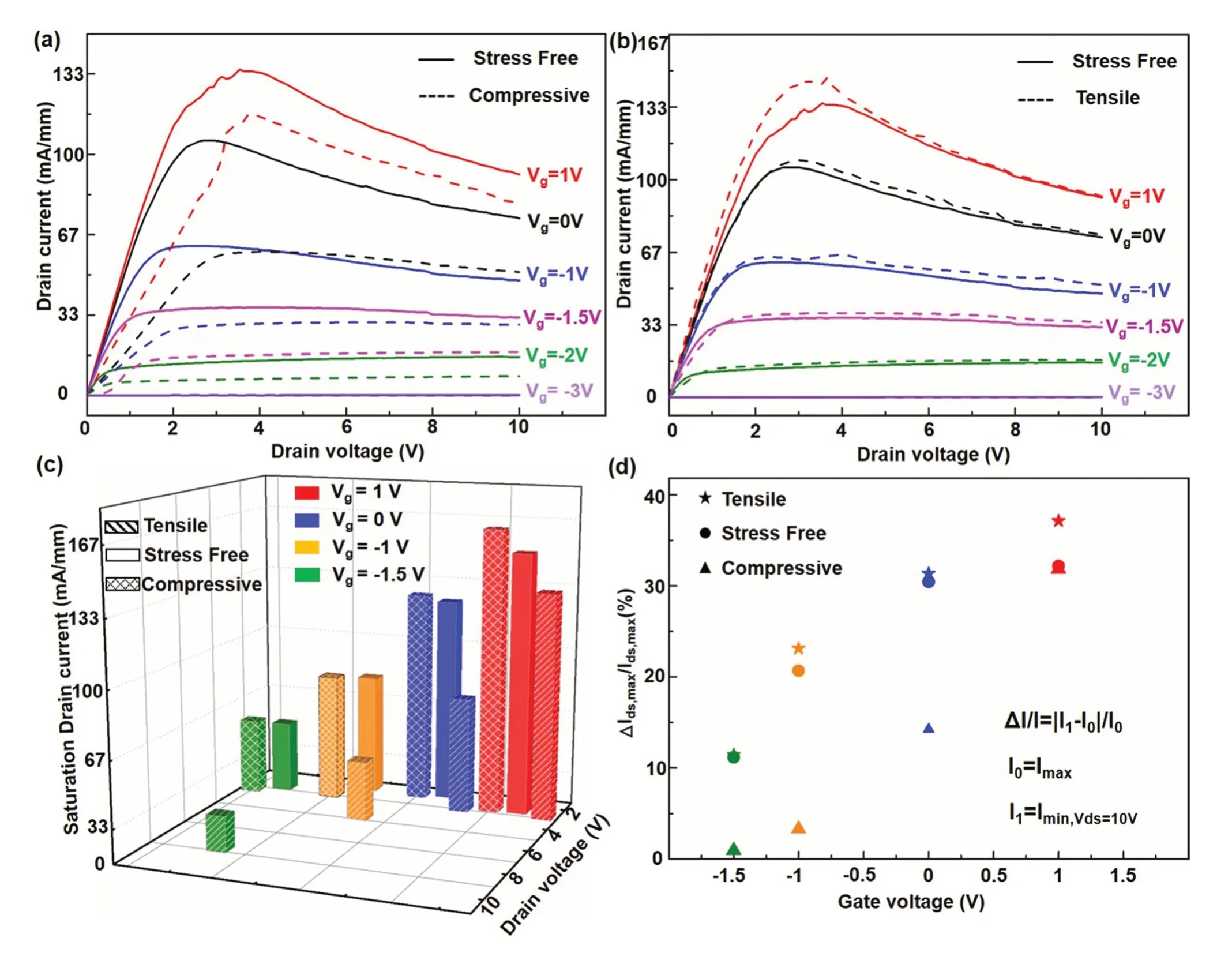
Fig.5 Piezotronic effect and investigate on saturation drain current attenuation. a I-V characteristics of HEMTs under strain free, compressive and b tensile strain condition. c The saturation drain current value and the corresponding peak position changes. d The corresponding relative changes (ΔIds,max/Ids,max)


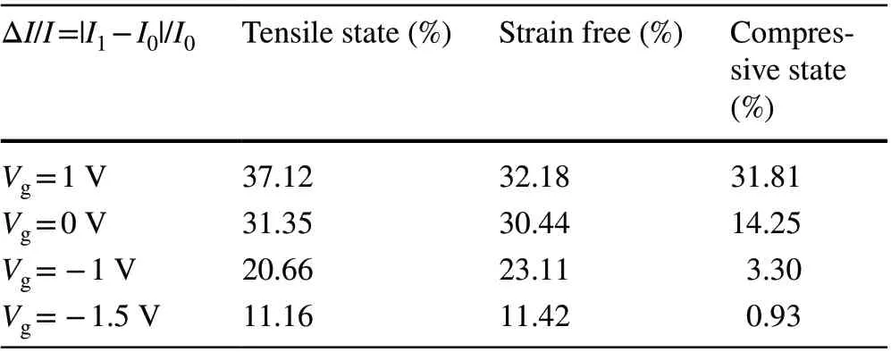
Table 3 The relative change of saturation drain current attenuation
3.3 Physical Mechanisms

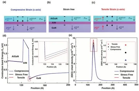
Fig.6 Working mechanism of the piezotronic effect and Self-consistent calculation of energy profiles and 2DEG sheet density. The coupling of piezotronics-induced polarization and intrinsic polarization (psp;plm), corresponding energy band profiles, and distribution of 2DEG in AlGaN/AlN/GaN HEMTs under b strain free, a compressive and c tensile strain states. d The conduction band energy profiles under compressive strain state (blue line); stress free state (black line); tensile strain state (red line). e The sheet density of 2DEG under under compressive strain state (blue line); stress free state (black line); tensile strain state (red line)
4 Conclusion
ELCO technology was utilized to prepare flexible GaN HEMT arrays with a size of > 2cm2. The piezotronic effect was then introduced to the AlGaN/AlN/GaN heterostructure membrane as an effective approach to modulate the physical properties of the 2DEG and phonon in the HEMTs, and thus control the electron transport process and thermal conductivity. Compared to existing traditional methods, the piezotronic effect has particular advantages, introducing external stress exhibits unique advantages of convenience, cost and reliability. By coupling the piezotronic effect into the device, the saturation current increased by 3.15% under the 0.547% tensile state, while the thermal conductivity of the HEMTs was enhanced monotonously and significantly under the compressive strain state. The piezotronic effect on the 2DEG, thermal conductivity and the coupling between the external strain-induced Ppiezoand the intrinsic Pspand Plmwere demonstrated in detail to systematically explain the intrinsic mechanism. This study provides an in-depth understanding of the piezotronic-effect and endeavors to open new ways for thermal management, with practical applications in flexible electronics.
AcknowledgementsThis research was supported by Key-Area Research and Development Program of Guangdong Province (Nos. 2020B010172001, 2020B010174004), GDAS’ Project of Science and Technology Development(No. 2018GDASCX-0112), Science and Technology Program of Guangzhou (No. 2019050001), National Key Research and Development Program of China (No. 2017YFB0404100), National Natural Science Foundation of China (Grant No. 11804103) and Guangdong Natural Science Foundation for Distinguished Young Scholars (Grant No. 2018B030306048).
Open AccessThis article is licensed under a Creative Commons Attribution 4.0 International License, which permits use, sharing, adaptation, distribution and reproduction in any medium or format, as long as you give appropriate credit to the original author(s) and the source, provide a link to the Creative Commons licence, and indicate if changes were made. The images or other third party material in this article are included in the article’s Creative Commons licence, unless indicated otherwise in a credit line to the material. If material is not included in the article’s Creative Commons licence and your intended use is not permitted by statutory regulation or exceeds the permitted use, you will need to obtain permission directly from the copyright holder. To view a copy of this licence, visit http://creat iveco mmons.org/licen ses/by/4.0/.
Supplementary InformationThe online version contains supplementary material available at (https://doi.org/10.1007/s4082 0-021-00589-4).
杂志排行
Nano-Micro Letters的其它文章
- Interior and Exterior Decoration of Transition Metal Oxide Through Cu0/Cu+ Co-Doping Strategy for High-Performance Supercapacitor
- Lead-Free Perovskite Materials for Solar Cells
- Berlin Green Framework-Based Gas Sensor for Room-Temperature and High-Selectivity Detection of Ammonia
- Highly Sensitive Ultrathin Flexible Thermoplastic Polyurethane/Carbon Black Fibrous Film Strain Sensor with Adjustable Scaffold Networks
- A Review on Metal-Organic Framework-Derived Porous Carbon-Based Novel Microwave Absorption Materials
- Ultrasonic Plasma Engineering Toward Facile Synthesis of Single-Atom M-N4/N-Doped Carbon (M = Fe, Co) as Superior Oxygen Electrocatalyst in Rechargeable Zinc-Air Batteries
